Effects of Experimental Configuration on the Morphology of Two-Dimensional ZnO Nanostructures Synthesized by Thermal Chemical-Vapor Deposition


Abstract
1. Introduction
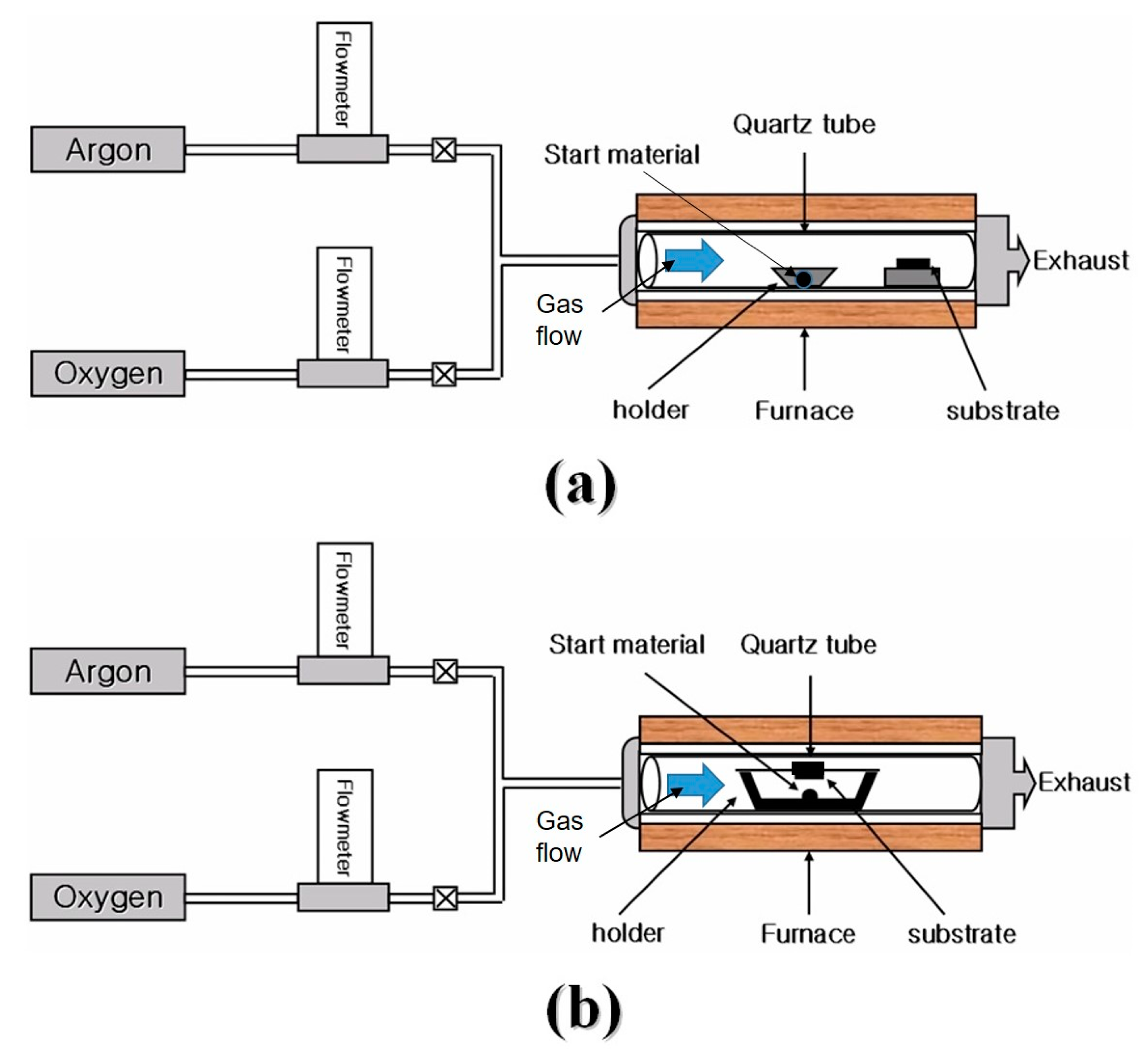
2. Experiments
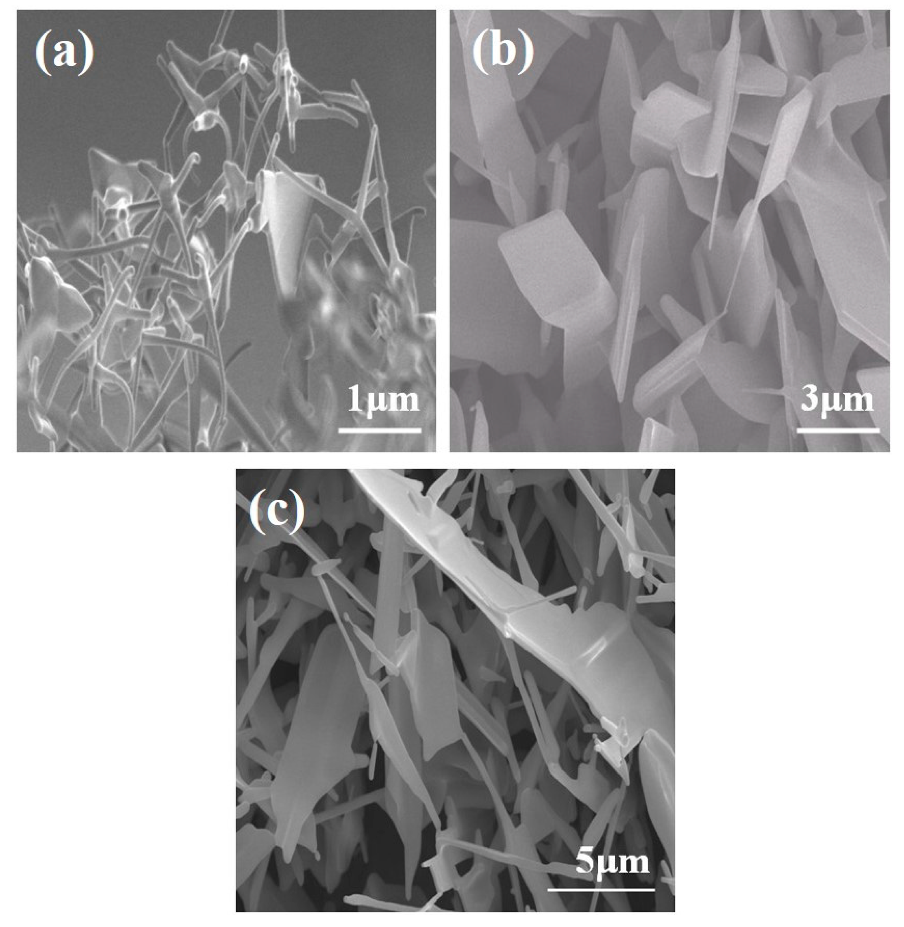
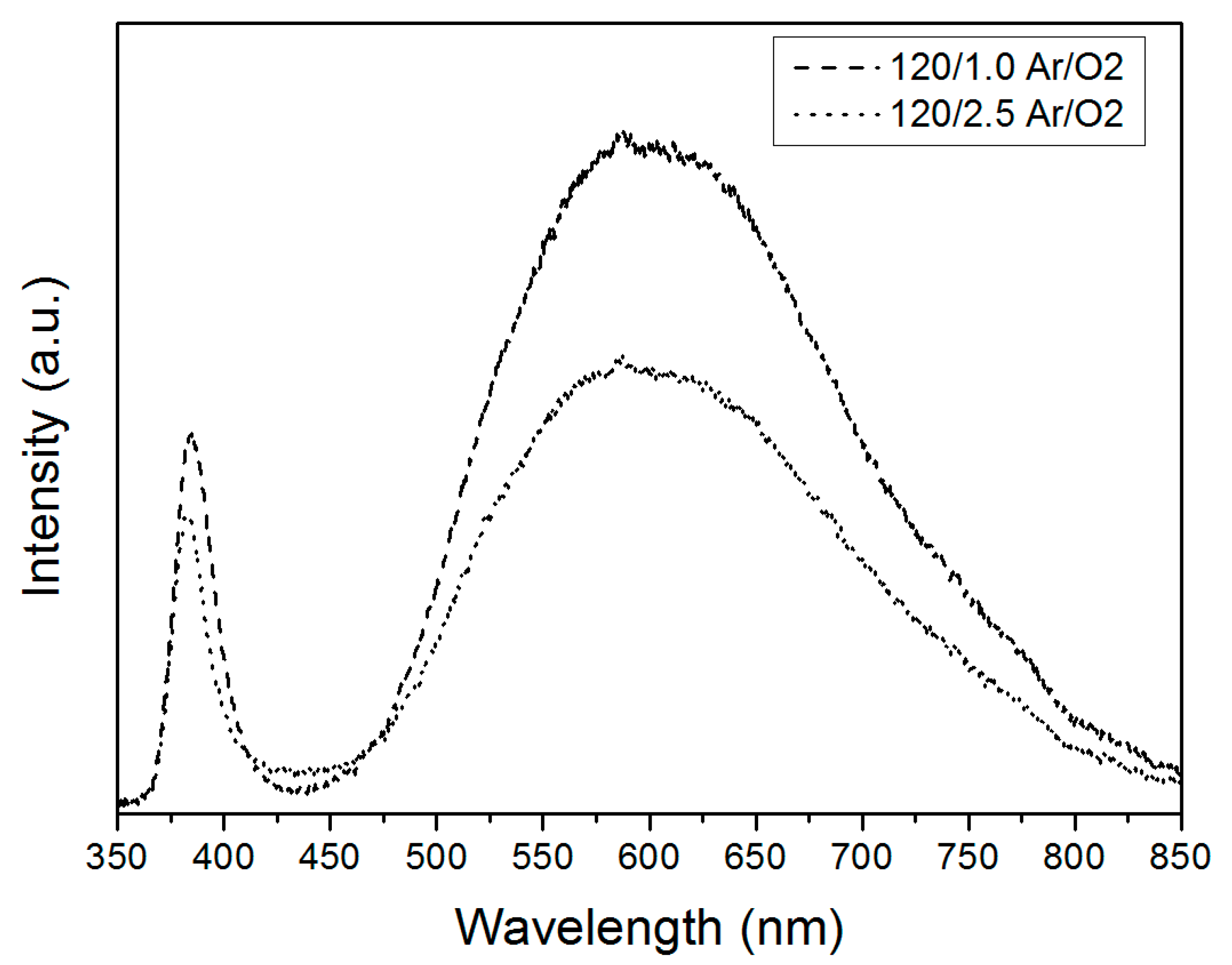
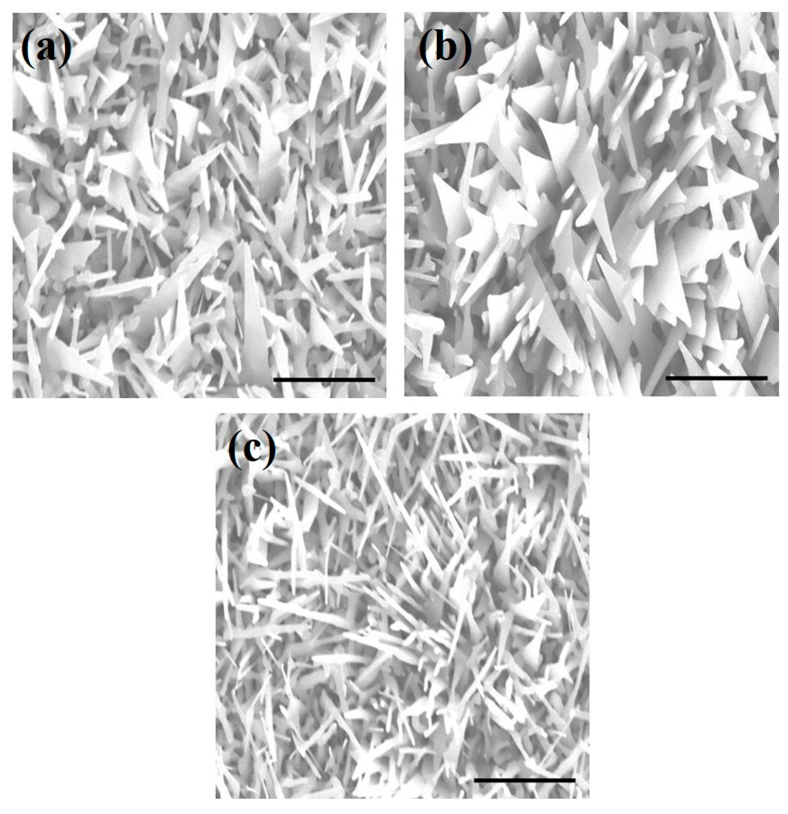
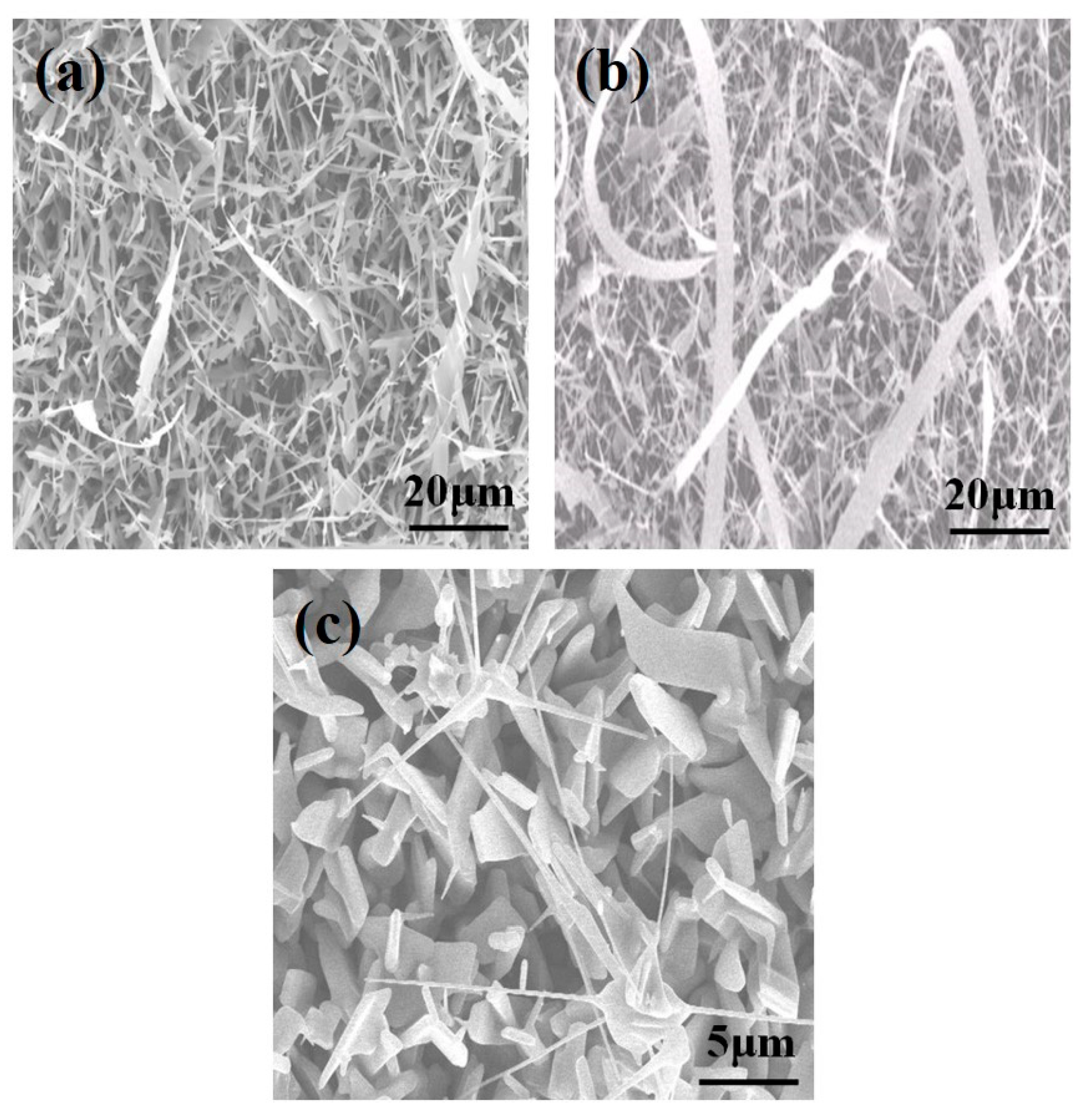
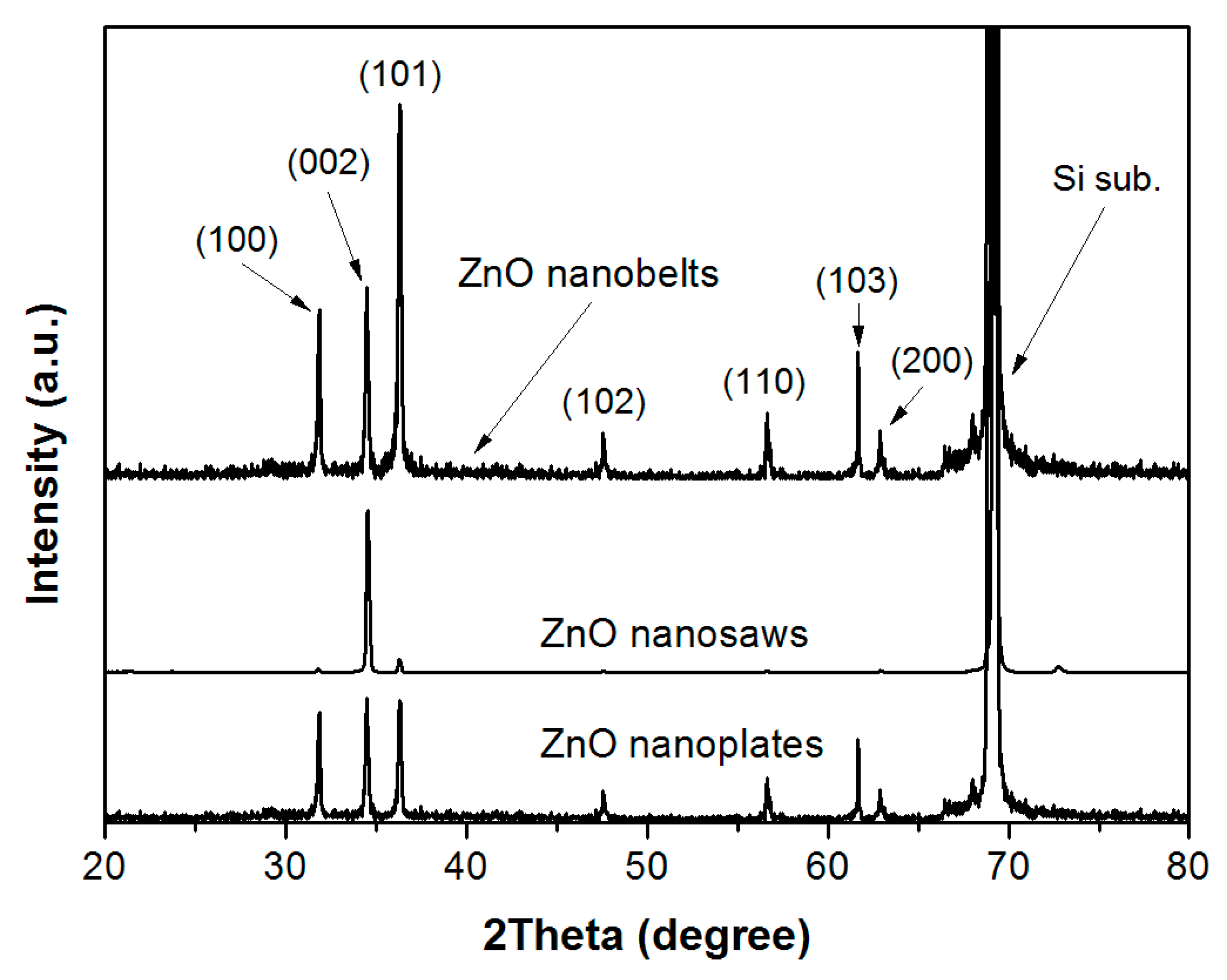
3. Results and Discussion
4. Conclusions
Author Contributions
Funding
Conflicts of Interest
References
- Kang, J.-W.; Kim, B.-H.; Song, H.; Jo, Y.-R.; Hong, S.-H.; Jung, G.Y.; Kim, B.-J.; Park, S.-J.; Cho, C.-H. Radial multi-quantum well ZnO nanorod arrays for nanoscale ultraviolet light-emitting diodes. Nanoscale 2018, 10, 14812–14818. [Google Scholar] [CrossRef] [PubMed]
- Mahmud, A.; Khan, A.A.; Voss, P.; Das, T.; Abdel-Rahman, E.; Ban, D. A High Performance and Consolidated Piezoelectric Energy Harvester Based on 1D/2D Hybrid Zinc Oxide Nanostructures. Adv. Mater. Interfaces 2018, 5, 1801167. [Google Scholar] [CrossRef]
- Wang, Q.; Yang, D.; Qiu, Y.; Zhang, X.; Song, W.; Hu, L. Two-dimensional ZnO nanosheets grown on flexible ITO-PET substrate for self-powered energy-harvesting nanodevices. Appl. Phys. Lett. 2018, 112, 63906. [Google Scholar] [CrossRef]
- Huang, M.H.; Mao, S.; Feick, H.; Yan, H.; Wu, Y.; Kind, H.; Weber, E.; Russo, R.; Yang, P. Room-Temperature Ultraviolet Nanowire Nanolasers. Science 2001, 292, 1897–1899. [Google Scholar] [CrossRef]
- Song, J.; Zhou, J.; Wang, Z.L. Piezoelectric and Semiconducting Coupled Power Generating Process of a Single ZnO Belt/Wire. A Technology for Harvesting Electricity from the Environment. Nano Lett. 2006, 6, 1656–1662. [Google Scholar] [CrossRef]
- Sadek, A.Z.; Wlodarski, W.; Li, Y.X.; Yu, W.; Li, X.; Yu, X.; Kalantar-Zadeh, K. A ZnO nanorod based layered ZnO/64 YX LiNbO3 SAW hydrogen gas sensor. Thin Solid Films 2007, 515, 8705. [Google Scholar] [CrossRef]
- Law, M.; Greene, L.E.; Johnson, J.C.; Saykally, R.; Yang, P. Nanowire dye-sensitized solar cells. Nat. Mater. 2005, 4, 455–459. [Google Scholar] [CrossRef]
- Sun, T.; Qiu, J.; Liang, C. Controllable Fabrication and Photocatalytic Activity of ZnO Nanobelt Arrays. J. Phys. Chem. C 2008, 112, 715–721. [Google Scholar] [CrossRef]
- Snure, M.; Tiwari, A. Synthesis, Characterization, and Green Luminescence in ZnO Nanocages. J. Nanosci. Nanotechnol. 2007, 7, 481–485. [Google Scholar] [CrossRef]
- Wang, J.X.; Sun, X.W.; Wei, A.; Lei, Y.; Cai, X.P.; Li, C.M.; Dong, Z.L. Zinc oxide nanocomb biosensor for glucose detection. Appl. Phys. Lett. 2006, 88, 233106. [Google Scholar] [CrossRef]
- Ko, S.H.; Lee, S.; Kang, H.W.; Nam, K.H.; Yeo, J.; Hong, S.J.; Grigoropoulos, C.P.; Sung, H.J. Nanoforest of Hydrothermally Grown Hierarchical ZnO Nanowires for a High Efficiency Dye-Sensitized Solar Cell. Nano Lett. 2011, 11, 666–671. [Google Scholar] [CrossRef]
- Tan, C.; Zhang, H. Wet-chemical synthesis and applications of non-layer structured two-dimensional nanomaterials. Nat. Commun. 2015, 6, 7873. [Google Scholar] [CrossRef]
- Pung, S.-Y.; Choy, K.-L.; Hou, X. Tip-growth mode and base-growth mode of Au-catalyzed zinc oxide nanowires using chemical vapor deposition technique. J. Cryst. Growth 2010, 312, 2049–2055. [Google Scholar] [CrossRef]
- Iwan, S.; Zhao, J.; Tan, S.; Sun, X. Enhancement of UV photoluminescence in ZnO tubes grown by metal organic chemical vapour deposition (MOCVD). Vacuum 2018, 155, 408–411. [Google Scholar] [CrossRef]
- Wu, L.; Wu, Y.; Lu, W. Preparation of ZnO Nanorods and optical characterizations. Phys. E Low Dimens. Syst. Nanostruct. 2005, 28, 76–82. [Google Scholar] [CrossRef]
- Kennedy, O.W.; Coke, M.L.; White, E.R.; Shaffer, M.; A Warburton, P. MBE growth and morphology control of ZnO nanobelts with polar axis perpendicular to growth direction. Mater. Lett. 2018, 212, 51–53. [Google Scholar] [CrossRef]
- Son, H.J.; Jeon, K.A.; Kim, C.E.; Kim, J.H.; Yoo, K.H.; Lee, S.Y. Synthesis of ZnO nanowires by pulsed laser deposition in furnace. Appl. Surf. Sci. 2007, 253, 7848–7850. [Google Scholar] [CrossRef]
- Menzel, A.; Subannajui, K.; Bakhda, R.; Wang, Y.; Thomann, R.; Zacharias, M. Tuning the Growth Mechanism of ZnO Nanowires by Controlled Carrier and Reaction Gas Modulation in Thermal CVD. J. Phys. Chem. Lett. 2012, 3, 2815–2821. [Google Scholar] [CrossRef]
- Wang, Z.L. Zinc oxide nanostructures: Growth, properties and applications. J. Phys. Condens. Matter 2004, 16, R829. [Google Scholar] [CrossRef]
- Park, J.H.; Park, J.G. Synthesis of ultrawide ZnO nanosheets. Curr. Appl. Phys. 2006, 6, 1020. [Google Scholar] [CrossRef]
- Wagner, R.S.; Ellis, W.C. Vapor-Liquid-Solid Mechanism of Single Crystal Growth. Appl. Phys. Lett. 1964, 4, 89. [Google Scholar] [CrossRef]
- Huang, M.H.; Wu, Y.; Feick, H.; Tran, N.; Weber, E.; Yang, P. Catalytic Growth of Zinc Oxide Nanowires by Vapor Transport. Adv. Mater. 2001, 13, 113. [Google Scholar] [CrossRef]
- Sekar, A.; Kim, S.H.; Umar, A.; Hahn, Y.B. Catalyst-free synthesis of ZnO nanowires on Si by oxidation of Zn powders. J. Cryst. Growth 2005, 277, 471. [Google Scholar] [CrossRef]
- Wu, C.C.; Wuu, D.S.; Lin, P.R.; Chen, T.N.; Horng, R.H. Three-Step Growth of Well-Aligned ZnO Nanotube Arrays by Self-Catalyzed Metalorganic Chemical Vapor Deposition Method. Cryst. Growth Des. 2009, 9, 4555. [Google Scholar] [CrossRef]
- Wu, C.C.; Wuu, D.; Lin, P.R.; Chen, T.N.; Horng, R.H. Realization and Manipulation of ZnO Nanorod Arrays on Sapphire Substrates Using a Catalyst-Free Metalorganic Chemical Vapor Deposition Technique. J. Nanosci. Nanotechnol. 2010, 10, 3001–3011. [Google Scholar] [CrossRef] [PubMed]
- Kong, Y.C.; Yu, D.P.; Zhang, B.; Fang, W.; Feng, S.Q. Ultraviolet-emitting ZnO nanowires synthesized by a physical vapor deposition approach. Appl. Phys. Lett. 2001, 78, 407–409. [Google Scholar] [CrossRef]
- Vanheusden, K.; Warren, W.L.; Seager, C.H.; Tallant, D.R.; Voigt, J.A.; Gnade, B.E. Mechanisms behind green photoluminescence in ZnO phosphor powders. J. Appl. Phys. 1996, 79, 7983–7990. [Google Scholar] [CrossRef]
- Wang, Z.L.; Kong, X.Y.; Zuo, J.M. Induced Growth of Asymmetric Nanocantilever Arrays on Polar Surfaces. Phys. Rev. Lett. 2003, 91, 185502. [Google Scholar] [CrossRef]
- Gao, P.X.; Lao, C.S.; Ding, Y.; Wang, Z.L. Metal/Semiconductor Core/Shell Nanodisks and Nanotubes. Adv. Funct. Mater. 2006, 16, 53–62. [Google Scholar] [CrossRef]
- Pan, Z.; Dai, Z.R.; Wang, Z.L. Nanobelts of Semiconducting Oxides. Science 2001, 291, 1947–1949. [Google Scholar] [CrossRef]
- Kong, B.H.; Cho, H. Formation of vertically aligned ZnO nanorods on ZnO templates with the preferred orientation through thermal evaporation. J. Cryst. Growth 2006, 289, 370–375. [Google Scholar] [CrossRef]
- Martensson, T.; Borgstrom, M.T.; Seifert, W.; Ohlsson, J.; Samuelson, L. Fabrication of individually seeded nanowire arrays by vapour–liquid–solid growth. Nanotechnology 2003, 14, 1255. [Google Scholar] [CrossRef]


© 2020 by the authors. Licensee MDPI, Basel, Switzerland. This article is an open access article distributed under the terms and conditions of the Creative Commons Attribution (CC BY) license (http://creativecommons.org/licenses/by/4.0/).
Share and Cite
Choi, S.C.; Lee, D.K.; Sohn, S.H. Effects of Experimental Configuration on the Morphology of Two-Dimensional ZnO Nanostructures Synthesized by Thermal Chemical-Vapor Deposition. Crystals 2020, 10, 517. https://doi.org/10.3390/cryst10060517
Choi SC, Lee DK, Sohn SH. Effects of Experimental Configuration on the Morphology of Two-Dimensional ZnO Nanostructures Synthesized by Thermal Chemical-Vapor Deposition. Crystals. 2020; 10(6):517. https://doi.org/10.3390/cryst10060517
Chicago/Turabian StyleChoi, Seok Cheol, Do Kyung Lee, and Sang Ho Sohn. 2020. "Effects of Experimental Configuration on the Morphology of Two-Dimensional ZnO Nanostructures Synthesized by Thermal Chemical-Vapor Deposition" Crystals 10, no. 6: 517. https://doi.org/10.3390/cryst10060517
APA StyleChoi, S. C., Lee, D. K., & Sohn, S. H. (2020). Effects of Experimental Configuration on the Morphology of Two-Dimensional ZnO Nanostructures Synthesized by Thermal Chemical-Vapor Deposition. Crystals, 10(6), 517. https://doi.org/10.3390/cryst10060517