Article

Synthesis of a Novel In2O3-InN Bottle Nanotube Using In-Situ Partial Oxidation with Enhanced Gas Sensing Platform to Detect NO2

1
State Key Joint Laboratory of Integrated Optoelectronics, College of Electronic Science and Engineering, Jilin University, Changchun 130012, China
2
College of Earth Sciences, Jilin University, Changchun 130061, China
*
Author to whom correspondence should be addressed.
Crystals 2020, 10(7), 570; https://doi.org/10.3390/cryst10070570
Submission received: 21 May 2020 / Revised: 26 June 2020 / Accepted: 30 June 2020 / Published: 2 July 2020
(This article belongs to the Special Issue Functional Oxide Based Thin-Film Materials (Volume II))

Abstract

:
A brand-new gas sensor nanocomposite, In2O3-InN, was synthesized by in-situ partial oxidation of InN and presented fast response–recovery property for NO2 detecting. The structure and morphology of the samples were characterized by X-ray diffraction (XRD), scanning electron microscopy (SEM), transmission electron microscopy (TEM), X-ray photoelectron spectroscopy (XPS) and energy-dispersive X-ray detection (EDX) analysis. The results show that the final In2O3-InN composites were composed of hexagonal type In2O3 and hexagonal type InN, which exhibited bottle nanotube structure on the relative macroscopic level. Microscopically, at the interface of In2O3 and InN, n–n hetero junction formed. Works form gas sensing property found that it is obviously that In2O3-InN got a quite stronger response, 1021, at relatively lower temperature, 100 °C, comparing to pure In2O3, 279.1 at 150 °C. After doping, the gas-sensing performance was improved. By analyzing the concentration of oxygen vacation and n–n hetero junctions mechanism, it was verified that the superiority of gas sensing properties of the In2O3-InN can be attributed to the high concentration of oxygen vacancies and the formation of n–n hetero junctions.

1. Introduction

Nitrogen peroxide is one of the three pollutants included in the air quality required by the National Environmental Protection Administration [1]. It mainly comes from the combustion of fuel and city automobile exhaust. Industrial production processes can also produce some nitrogen dioxide [2]. With the increasingly serious air pollution, the monitoring situation of major atmospheric pollutants such as nitrogen oxides is becoming increasingly severe, and the sensitivity and anti-interference requirements for the NO2 detection system are also increasing. With the development of new technology, new energy and new materials [3], the difficulty of preparing new functional materials that are completely different from traditional materials has become increasingly apparent [4]. How to synthesize new composite materials on the basis of traditional materials has gradually become the breakthrough point of current materials science [5].
In recent years, the air sensitive transmitter with the semi-conducting body oxygenated material as the raw material has attracted attention. Semiconductor oxides such as SnO2, WO3, In2O3, TiO2 and ZnO are usually used as sensors to monitor NO2 [6]. However, for these high-resistance materials [7], which are all n-type conductance characteristics, the oxidizing gas will make its electrical resistance further increase. It is easy to over shoot the measuring range of the electric resistance, making accurate measurements difficult [8]. Different dopants can provide a surface area which is conductive to gas–gas and gas–solid reactions on the semiconductor surface, thus improving the sensitivity of the sensor.
As one of the ideal gas sensing materials, In2O3 has been exhaustively investigated during the past decades and exhibits excellent sensitivity to multifarious gases [9]. However, because of the inherent nature of In2O3, i.e., its wide band gap [10], it cannot always present expected sensitivity and resistance, particularly in the low gas concentration environment [11]. Lu et al. used sol–gel method combined with electrostatic spinning technology to prepare indium oxide nanometer ceramic fiber with a diameter of 20–50 nm [12].Chen et al. [13] used a solvothermal method at 300 °C to prepare InOOH nanotubes and calcined to obtain metastable single crystal hexagonal In2O3 nanotubes. With the prosperity of modern technology, more precise fundamental properties of InN, including narrow band gap and surface electron charge accumulation, were exposed [14]. There are many ways to prepare InN materials, including simple chemical methods. Brigit Schwenzer et al. prepared InN nanomaterials with different morphology at different temperatures by CVD method [15]. Luo et al. prepared a method using indium nitride oxide powder, InN nanoribbons and nanotube structures [16]. As reported, narrow band gap (0.6–0.7 eV), excellent electron transport and high electron density endow InN prominent electoral properties [17]. Thus, mixing InN and In2O3 into brand new composites could theoretically ameliorate their weaknesses and boost their respective merits.
Inspired by this, we synthesized a gas sensor based on InN–In2O3 composite hetero structure, which has not been previously reported. An In2O3−InN composite was employed as a gas sensor on the sensing platform to detect NO2. Then, we studied different gas sensing mechanisms of In2O3 and In2O3-InN composite by analyzing the concentration of oxygen vacancies and the n–n hetero junctions mechanism through transmission electron microscopy (TEM) and X-ray photoelectron spectroscopy (XPS) methods to discover the reason for gas property enhancement.

2. Materials and Methods

2.1. Reagents and Instruments

In(NO3)3 was from Macklin Reagent Chemical Company (Shanghai, China), citric acid was from Chemical Reagent Factory (Jilin, China) and ammonia water was from Airichem Special Gas Chemical Co., Ltd. (Dalian, China).
The following four instruments were used in the preparation of this experiment: KSY-419 box resistance furnace (Energy-saving Electric Furnace Factory, Shenyang, China); T09-1S magnetic stirrer (Sile Instrument, Shanghai, China); OTF-1200X vacuum tube type high temperature sintering furnace (Kejing Material Technology Co., Ltd., Hefei, China); and SK-G08123K vacuum tube type high temperature oxidation furnace (Zhonghuan Experimental Instrument Factory, Tianjin, China).
X-ray diffraction (XRD) experiments were operated on a Rigaku D-Max 2550 X-ray diffract to meter with Cu Kαλ = 1.5418 Å, scanning range 20–80° and scanning speed 4°/min at 40 kA and 40 mA. The Scanning electron microscopy (SEM PHILIPS XL-30) (JEOL, Beijing, China) and energy dispersive spectrometry (EDS XD-3) (Shimadzu, Shanghai, China) analyses were performed on a (JEOL, Beijing, China) JSM-7500F ESEM FEG scanning electron microscopy. High-resolution transmission electron microscopy (HRTEM) (Micromeritics, Shanghai, China) and selected area electron diffraction were carried out on a ASAP2010M transmission electron microscope. XPS analyses were performed on an ESCALAB 250 spectrometer (Thermo Fisher Scientific, Shanghai, China).

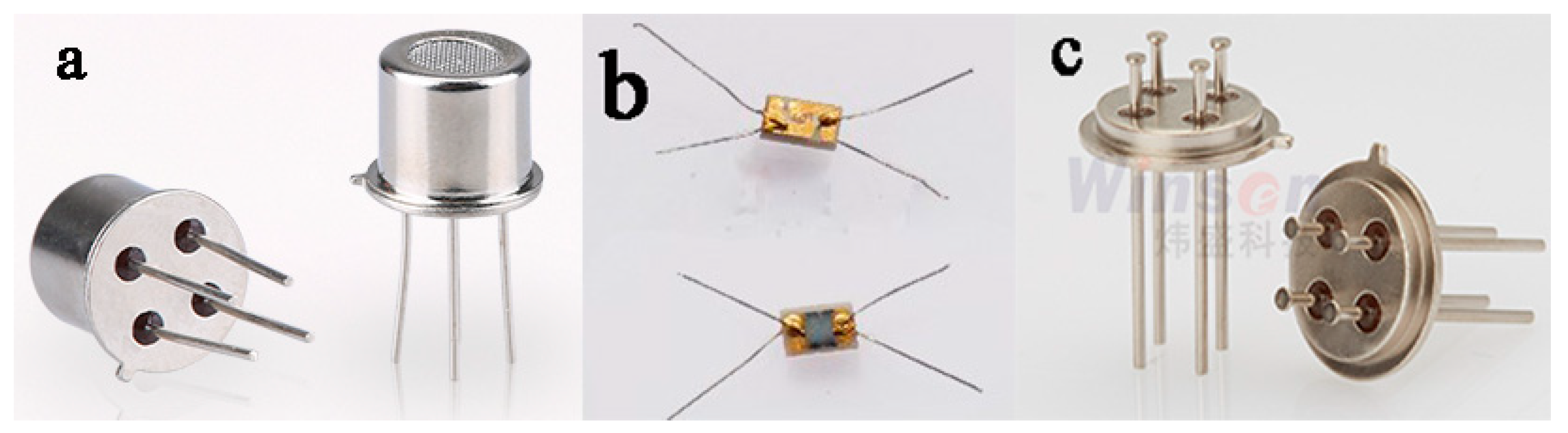
2.2. Fabrication and Measurement

The In2O3-InN nanocomposite was prepared based on an InN substrate material. Therefore, in the experiment, a material growth process of nitriding first and then oxidizing was adopted. In2O3 was nitride by using a vacuum tube furnace, and an InN base layer was grown on the ceramic sheet. Firstly, the precursor In2O3 powder was prepared. The process is as follows: At 0.1 mol/L, In(NO3)3 and citric acid were mixed at a molar ratio of 1:2, and then ammonia water was added drop wise with stirring to adjust the pH to 6 to obtain a brownish yellow transparent solution. The gel was evaporated to dryness in a 75 °C water bath. The gel was further dried in an oven at 85 °C, and then it was calcined in a resistance furnace at 600 °C for 2 h to obtain nanometer In2O3.
The nitriding process is as follows: The prepared nano-In2O3 was spin-coated on a ceramic sheet, placed in a flat-bottomed quartz boat, which was placed in a tube furnace, passing NH3 (pressure 0.05 MPa, flow rate 10 Pa L/h), and heated for 55 min The temperature was maintained at 550 °C for 48 h, and then the temperature was naturally reduced to 20 °C to obtain a pure InN structure base material. Because the In powder was used to prepare the precursor, and the secondary nitriding temperature was high, a small amount of In elemental was easily precipitated, thus the In elementary substance was removed by using a centrifuge when preparing the final product.
Oxidation process: InN material was spin-coated on a ceramic sheet to make an InN substrate. The vacuum tube furnace was heated to 480 °C for 240 min, the InN substrate was pushed into the center of the tube furnace and O2 was oxidized for 25 min to fill N2. It was cooled to room temperature to prevent surface cracking. In2O3-InN nanocomposite was prepared.
This experiment used a miniature planar chip sensor, as shown in Figure 1a. As shown in Figure 1b, it has the advantages of larger effective reaction area than ceramic tube contact gas, stronger adhesion material and easier control and uniformity of spin coating material thickness. The main production process was mixing the prepared composite material with distilled water and spin-coating it on a 1.0 mm × 3.0 mm micro flat electrode pad printed with gold paste and connected to a platinum wire, and then welding it onto a metal four-pin socket, as shown in Figure 1c. To improve the mechanical stability of the prepared sensor, the device was sintered in a muffle furnace for 6 h. To prevent re-oxidation, the sintering temperature was controlled at 250 °C.
Device manufacturing process: The prepared material was mixed and uniformly spin-coated on 1.5 mm × 1.5 mm electrode pads (printed with gold paste, connected with platinum wire) with distilled water, and welded onto a metal four-pin socket.
Aging process: The prepared sensor was put on a four-pin electrode aging test bench, first aging (75 °C) for 24 h, resting for 24 h, second aging (100 °C) for 24 h, and leaving for 24 h three times (75 °C). After 24 h of standing, the gas sensitivity test was performed.
The gas sensitivity test instrument was a KGS101H-R500Mtype gas sensitivity detector, which was used to measure the electrical characteristics of the senor. The test method was static test method. A certain amount of gas or liquid was injected into a glass bottle and mixed with air to prepare a target gas of a certain concentration. There were two bottles, one for measuring air resistance. When the sensitivity of the sensor in the air became stable, the resistance was recorded as Ra. The other bottle measured the gas resistance; the sensor was removed and quickly placed into a volumetric flask filled with the target gas. When the resistance became stable, the value was denoted as Rg. As shown in Figure 2, the reason for the two volumetric bottles is that we must ensure that the air resistance and gas resistance sensors tested are the same. Ra/Rg is the sensitivity of the sensor in the target gas [18]. The response–recovery time is the time required for the gas sensor to measure the gas until the resistance change reaches 90% of its equilibrium value. When the gas sensor is transferred from the measured gas to the air, the time required for its equilibrium resistance to reach 10% is the recovery time.

3. Results

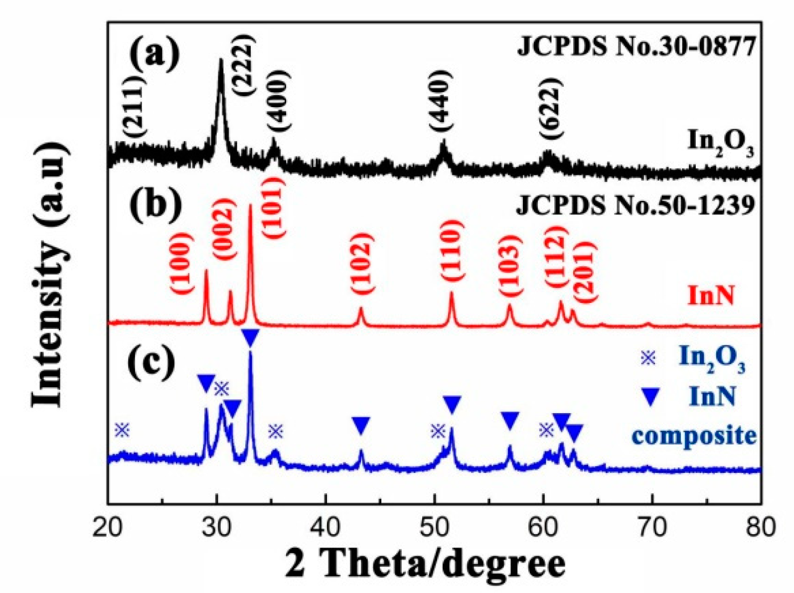
3.1. Materials Characterization

XRD patterns of In2O3, InN and In2O3-InN composites with graded structure are inserted in Figure 3. As shown in Figure 3a, the diffraction peaks at (211), (222), (400) and (622) belong to the In2O3 phase of the hexagonal type (JCPDS No. 30-0877).
The diffraction peaks of (100), (002), (101), (102) and (110) also belong to the hexagonal type InN (JCPDS No. 50-1239), as shown in Figure 3. In addition, the clear and strong peaks indicate that the InN is highly crystalline. In comparison, the peaks representing hexagonal structured In2O3 did not shift in the In2O3-InN samples, which revealed that the doping of InN only occurred on the surface of the In2O3 and did not damage the crystal structure of In2O3. Figure 3c shows that the composite of hexagonal structured In2O3 and hexagonal structured InN, and there is no change of crystal type. No other heterozygous peaks are present, indicating that these are pure phase composite.
Furthermore, according to Scherrer formula, the average grain sizes of prepared pure InN and In2O3 are 29.4 and 62.4 nm, respectively. The average grain size of conventional In2O3-InN composite is 30 nm, calculated via the Debye–Scherrer formula. The reason for the grain size reduction is that the oxidation process on InN substrate can control the grain growth.
The grain size of the composite materials of In2O3-InN is smaller than materials of In2O3. It can be concluded that the combination of the two materials would help improve the gas sensing performance.
Figure 4 shows SEM images of In2O3 (Figure 4a), InN (Figure 4b) and In2O3-InN (Figure 4c,d). In Figure 4a, it can be seen clearly that the morphology is flower-shaped In2O3 with obvious hierarchy, which was formed by assembly of two-dimensional sheet In2O3. Moreover, the two-dimensional pieces have regular morphology, uniform size and obvious uniform distribution of regular structure on the surface. The flower structure is made of particles of about 60 nm in size. Figure 4b shows the enlarged SEM images of InN substrate at high resolution. A smooth octahedral InN microstructure can be seen.
Figure 4c,d shows the high-resolution magnification SEM image of In2O3-InN bottle nanotube material. The morphologies of the composite changed from original octahedral structure to bottle structure. The average diameter of In2O3 nanoparticles was 35 nm and that of the In2O3-InN nanocomposite was 25 nm; the doping of InN effectively decreased the average diameter of In2O3 nanoparticles. Owing to the poor sensitivity and high resistance of In2O3, combining InN with In2O3, the oxidized material of which presents a nanocomposite cavity structure, can better improve the gas sensitivity.
The InN and In2O3-InN nanocomposite were evaluated by EDX analysis technique, as shown in Figure 4e,f, respectively. The results reveal that no impurity element can be detected.
TEM images of InN and In2O3-InN are depicted in Figure 5. Figure 5a shows that there is a slight agglomeration of InN nanoparticles with 25.6 nm, and InN presents hexagonal structure. According to Figure 5b, the composite of In2O3-InN is bottle-like structure. Figure 5c is the corresponding HRTEM (High Resolution Transmission Electron Microscope) image. As can be seen, the well-defined lattice spacings between the two are 0.398 and 0.307 nm, both of which exhibit well-defined lattice fringes. More specifically, the two correspond to the inter-planar distance between faces of In2O3 (222) and InN (002).
The material composition of nanomaterial and the valence state of elements were investigated by XPS analysis. In the full spectra, as shown in Figure 6a, all the Gaussian deconvolution peaks could be attributed to In, N, C and O (four different elements), and no other kind of elements was discovered. The C 1s peak was assigned an adventitious C binding energy peak and was used as a reference for calibration at 284.5 eV. In Figure 6b, the binding energies of In3d5/2 and In3d3/2 of In2O3-InN are 451.7 and 444.1 eV, respectively. The binding energies of In3d5/2 and In3d3/2 in In2O3 are 451.9 and 444.3 eV, respectively, which are approximately 0.2 eV higher than that of In2O3-InN, revealing that In also existed in the form of In3+ in the developed materials. The migration of the binding energies in In2O3 and In2O3-InN is powerful evidence of electron-donating and electron-drawing structures in InN and In2O3, which is the proof of the presence of In2O3-InN n–n hetero structures. In the process of recombination, the bond energy of In-O bond increases, the oxidation ability increases and the bond energy of In-N bond decreases. Considering the above discussion, the binding energy of In has a redshift, resulting in In2O3-InN n–n hetero structures. As shown in Figure 6c, the peak of N1s of In2O3-InN is 398.8 eV, while the peak of N1s of InN is 397.8 eV. The latter is slightly lower than the former, which should be related to In-N bond, indicating the existence of n–n hetero junction. In Figure 6d, the In2O3 fitted peak was at 532.5 eV. The fitted peak at 531.5 eV corresponded to adsorbed O or OH species and the peak at 530.5 eV for In2O3 belonged to lattice O. The O 1s fitted peak of the In2O3-InN nanocomposite, at 529.7eV, was assigned to lattice O; the fitted peak at 530.5eV corresponded to adsorbed O or OH species; and the fitted peak at 532.0eV corresponded to O vacancies. The oxygen vacancy easily combined with chemically adsorbed O or OH species, which were significant for the gas sensing reaction. Because O atoms occupy different chemical environments in the two samples, each kind of fitted peak had its own shift in the In2O3InN nanocomposite. Figure 6d also shows the relative percentage of lattice O and adsorbed O in In2O3 and In2O3-InN as calculated from the Gaussian deconvolution peak integration areas. The relative percentages of lattice O, adsorbed O or OH species and O vacancies of In2O3 were 49.63%, 27.072% and 23.294%, respectively. These percentages for In2O3-InN were 16.78%, 38.95% and 44.27%, respectively. The relative percentage of O vacancies in In2O3-InN was higher than that of O vacancies in In2O3, and the relative percentage of O vacancies was greater in the In2O3-InN nanocomposite than inIn2O3 nanoparticles.

3.2. Gas Sensing Properties

Figure 7 is the response curves of as-prepared In2O3-InN, In2O3 and InN with respect to temperature when exposed to 50 ppm NO2. The figure shows that the sensitivity increased to the zenith between 25 and 100 °C and immediately reversed, showing a downward trend as the temperature continued to rise. Figure 7 shows that the responses of In2O3 increased between 25 and 150 °C, reaching its maximum, and then fell as the temperature decreased. Because of the doping of InN, gas sensitivity of In2O3-InN at the optimum temperature was decreased. Hence, choosing 100 °C as the optimum working temperature, batch experiments were plotted to verify the gas sensing properties. It is obviously that In2O3-InN gas sensors had optimum working temperature at 100 °C, namely, it had maximum sensitivity at 100°C In2O3-InN gas sensor’s maximum sensitivity towards 50 ppm NO2 was 1021 (Res = Ra/Rg). Likewise, In2O3 gas sensor had optimum working temperature at 150 °C, for which the maximum sensitivity was 279.1. In summary, after doping, the gas-sensing performance was improved.
We used the composite of In2O3-InN and In2O3 at 100 °C to explore the gas-sensing properties of varying NO2 concentrations of target gas. Figure 8a shows the sensitivity of In2O3-InN to different NO2 concentrations at the optimum test temperature (100 °C). Elevating the NO2 concentration enhanced the response intensity of the gas sensitivity of the material. More precisely, when the NO2 concentration was 1, 5, 10, 25 and 50 ppm, the In2O3-InN corresponding gas sensitivity was 18.8, 60.3, 165.1, 497.6 and 1021, respectively; however, the In2O3 corresponding gas sensitivity was 2.5, 11.4, 24.6, 130.2 and 279.1, respectively. Comparing with In2O3, the In2O3-InN sensors showed obvious superiority when the concentration of target gas was greater than 25 ppm. However, as the concentration fell beyond the 20-ppm threshold, the difference between two kinds of material was less obvious.
In addition, Figure 8b shows the comparison of response and recovery times between In2O3 and In2O3-InN. The response and recovery times of In2O3 were 2 and 1.5 s, while those of In2O3-InN were 1.5 and 2 s, which indicated that the In2O3-InN sensor had a higher response sensitivity but lower recovery sensitivity toward 50-ppm NO2 than the In2O3 sensor.
Selectivity is a vital parameter for characterizing the gas sensing properties of gas sensors. As shown in Figure 9, we tested the sensitivity of In2O3 and In2O3-InN gas sensors toward NO2, H2, SO2, CO, H2S and Cl2. The In2O3 gas sensor’s responses toward those vapors were 2.5, 1, 3, 1, 2 and 1 while the responses of In2O3-InN gas sensors were 60.3, 15.7, 3.5, 1.1, 1.6, 1.1 and 1.4. In2O3-InN showed a higher response than In2O3 for all tested gases NO2.
To figure out the causes of enhanced sensitivity of In2O3-InN toward NO2, we propose the following mechanism. As reported, as n-type semiconductors, the sensing mechanism of In2O3 and InN is tied closely with resistance variation attribute to absorption–desorption of oxygen molecules on the ostensible layer of the sensor oxides.
The electrical conductivity of the sensing material changes with the surface reaction of gas molecules during the adsorption and desorption process. In the initial state, the absorbed oxygen molecules get electrons from the In2O3 and then settle down at the channel surface in the form of O2−, O2 and O, as the reactions in Equations (1) and (2) [19]:
O2 (g) + e ⇄ O2− (ad)
O2– (ad) + e ⇄ O2− (ad)
The chemical absorbed oxygen species result in the formation of a surface depletion region. While the sensor is exposed in NO2, the NO2 molecules can not only get electrons from the In2O3 but also take electrons form the absorbed oxygen ions since the electron affinity of NO2 is 2.3 eV (strong oxidizing property), which is much higher than O2 (0.44 eV) and its related ions. The more and more free electrons captured by the NO2 injection reduces the total carriers and increases the thickness of electron depletion region, resulting in a sharp increase of the sensor resistance:
NO2 (g) + e ⇄ NO2 (ad)
When the sensor is put in air again, the resistance reduces to the initial value gradually with the desorption of NO2 molecules, and the released electrons return to the sensing material as free carriers:
NO2 (ad) ⇄ NO2 (g) + e
The characteristics of gas-sensitive sensors depends on the dimensions, particle size and morphology of the semiconductor nanomaterials. Recently, there have been several reports focused on the study of how to regulate the particle size and morphology for higher gas-sensitive performance [20]. Moreover, to significantly improve the fast response performance of new gas-sensitive sensors, one important way is to reduce the device size of the sensor by using advanced building technology with higher resolution and miniature chip structure. Promoting the charge conductivity of the gas-sensitive material is another way that should not be neglected [21]. Introducing N atoms to the lattices can accelerate the transfer of electrons and thus increase the conductivity [22].
Therefore, another positive aspect of the In2O3-InN sensor was the modulation of the potential barrier height. A potential barrier developed at n-In2O3/n-InN interfaces due to intrinsic potentials (Figure 10), and the potential barrier height at the n-In2O3 and n-InN interface was larger than that at the n-InN and n-InN interface during the adsorption and desorption of methanal vapor, which might be an additional benefit for the sensing properties.
When introducing InN into In2O3, hetero junction with Type I band alignment will form at the interface, where the energy of valence band edge of InN is higher than that of In2O3. It is convenient for electrons to transfer from the conduction bond of In2O3 to that of InN. InN is an n-type semiconductor; the concentration of electrons is far larger than that of holes. An EAL will form at the interface, resulting in a decrease in the initial resistance, and thereby an increase of sensitivity. Besides, as an electron withdrawing molecule, NO2 prefer to adsorb on electron-rich sites. Due to the heterogeneous structure formed at the interface between InN and In2O3, many defects will be introduced at the interface, including the dangling bond and NO bond of InN atoms, and the In–O bond energy will also be reduced [23]. These changes will absorb more NO2 gas and enhance the gas-sensitive performance.

4. Conclusions

An In2O3-InN composite was successfully prepared using in-situ partial oxidation synthesis. There is an n–n hetero junction structure at the two-phase interface of InN–In2O3 composite, which effectively improves the chemical microenvironment of the interface and applies it to the chip gas sensor. The result of gas sensitive characterization showed that In2O3-InN sensors have excellent sensitivity and selectivity for NO2 detection, as well as good response–recovery performance. The response to 50-ppm NO2 is 1021 and the response to 1-ppm NO2 is 18.8 at lower operating temperature of 100 °C. Due to the formation of a large amount of interface defect oxygen due to the formation of hetero junction structure, the increase in electron concentration and migration rate causes more electrons to react with the O2 adsorbed on the surface of the material to form more O and O ions. In the NO2 gas test, due to the lack of electrons in the material, it shows a large resistance in the air, which is the inherent reason the InN–In2O3 composite significantly improves the sensitivity of methanol detection.

Author Contributions

Author Contributions: Investigation, Y.W.; Methodology, G.W.; Software, Y.S.; Writing—original draft, Q.N.; Writing—review & editing, W.F. All authors have read and agreed to the published version of the manuscript.

Funding

This research was funded by National Natural Science Foundation of China (grant number No. 61774076) and the Science and Technology Development Program of Jilin Province, China (No. 20170101086JC).

Acknowledgments

We are grateful to all the authors for their contributions and financial help from the National Natural Science Foundation of China (grant number No. 61774076) and Science and Technology Development Program of Jilin Province, China (No. 20170101086JC).

Conflicts of Interest

The authors declare no conflict of interest.

References

  1. Khiabani, P.S.; Hosseinmardi, A.; Marzbanrad, E.; Ghashghaie, S.; Zamani, C.; Keyanpour-Rad, M.; Raissi, B. NO2 gas sensor fabrication through AC electrophoretic deposition from electrospun In2O3 nanoribbons. Sens. Actuators B Chem. 2012, 162, 102–107. [Google Scholar] [CrossRef]
  2. Singh, N.; Gupta, R.K.; Lee, P.S. Gold-nanoparticle-functionalized InO nanowires as CO gas sensors with a significant enhancement in response. Acs Appl. Mater. Interfaces 2011, 3, 2246. [Google Scholar]
  3. Liu, L.; Song, P.; Yang, Z.; Wang, Q. Ultra-fast responding C2H5OH sensors based on hierarchical assembly of SnO2 nanorods on cube-like alpha-Fe2O3. Sens. Actuators B Chem. 2018, 29, 5446–5453. [Google Scholar]
  4. Piot, D.; Smagghe, G.; Montheillet, F.J.M.S.F. Modeling of Grain-Boundary Mobility and Nucleation Rate During Discontinuous Dynamic Recrystallization in Ni-Nb Alloys and a High-Purity Alloy Derived from SAE 304L. Mater. Sci. Forum 2017, 879, 1501–1506. [Google Scholar] [CrossRef]
  5. Brigante, D.J.N. New composite materials. Nature 2014, 442, 282–286. [Google Scholar]
  6. Sharma, A.; Tomar, M.; Gupta, V. Enhanced response characteristics of SnO2 thin film based NO2 gas sensor integrated with nanoscaled metal oxide clusters. Sens. Actuators B Chem. 2013, 181, 735–742. [Google Scholar] [CrossRef]
  7. Capra, P.P.; Galliana, F.L.; Latino, M.; Bonavita, A.; Donato, N.; Neri, G. A High-Resistance Measurement Setup for MOX Sensing Materials Characterization. Sens. Microsyst. 2014, 268, 149–154. [Google Scholar]
  8. Shlimak, I.; Ginodman, V.; Gerber, A.B.; Milner, A.; Friedland, K.J.; Paul, D.J. Transverse “resistance overshoot” in a Si/SiGe two-dimensional electron gas in the quantum Hall effect regime. EPL 2005, 69, 997. [Google Scholar] [CrossRef]
  9. Waitz, T.; Wagner, T.; Sauerwald, T.; Kohl, C.D.; Tiemann, M. Ordered Mesoporous In2O3: Synthesis by Structure Replication and Application as a Methane Gas Sensor. Adv. Funct. Mater. 2009, 19, 653–661. [Google Scholar] [CrossRef]
  10. Pearton, S.J.; Ren, F.; Wang, Y.L.; Chu, B.H.; Chen, K.H.; Chang, C.Y.; Lim, W.; Lin, J.; Norton, D.P. Recent advances in wide bandgap semiconductor biological and gas sensors. Progess Mater. Sci. 2010, 55, 1–59. [Google Scholar] [CrossRef]
  11. Wei, D.; Huang, Z.; Wang, L.; Chuai, X.; Zhang, S.; Lu, G. Hydrothermal synthesis of Ce-doped hierarchical flower-like In2O3 microspheres and their excellent gas-sensing properties. Sens. Actuators B Chem. 2018, 255, 1211–1219. [Google Scholar] [CrossRef]
  12. Lu, Q.; Chen, D.; Jiao, X.; Liu, S. Research on preparation of In2O3 ceramic nanofiber mats by electrospinning and its gas sensing properties. J. Chem. Ind. Eng. 2011, 32, 1–4. [Google Scholar]
  13. Chen, C.; Chen, D.; Jiao, X.; Wang, C. Ultrathin corundum-type In2O3 nanotubes derived from orthorhombic InOOH: Synthesis and formation mechanism. Chem. Commun. 2006, 2006, 4632–4634. [Google Scholar] [CrossRef]
  14. Jahangir, I.; Wilson, A.; Uddin, M.A.; Chandrashekhar, M.V.; Koley, G. Oxygen plasma treated graphene/InN nanowire heterojunction based sensors for toxic gas detection. In Proceedings of the 2016 IEEE Sensors, Orlando, FL, USA, 30 October–3 November 2016; pp. 1–3. [Google Scholar]
  15. Schwenzer, B.; Loeffler, L.; Seshadri, R.; Keller, S.; Lange, F.F.; DenBaars, S.P.; Mishra, U.K. Preparation of indium nitride micro- and nanostructures by ammonolysis of indium oxide. J. Mater. Chem. 2004, 14, 637. [Google Scholar] [CrossRef]
  16. Luo, S.; Zhou, W.; Zhang, Z.; Dou, X.; Liu, L.; Zhao, X.; Liu, D.; Song, L.; Xiang, Y.; Zhou, J.; et al. Bulk-quantity synthesis of single-crystalline indium nitride nanobelts. Chem. Phys. Lett. 2005, 411, 361–365. [Google Scholar] [CrossRef]
  17. Wang, F.; Xue, C.; Zhuang, H.; Zhang, X.; Ai, Y.; Sun, L.; Yang, Z.; Li, H. Growth and characterization of the InN film ammonification technique. Phys. E Low-Dimens. Syst. Nanostruct. 2008, 40, 664–667. [Google Scholar] [CrossRef]
  18. Wang, B.; Zeng, Q.; Chen, S.; Yue, T.; Han, B.; Feng, W.; Yang, D. Preparation and Gas Sensing Performance of Hierarchical Porous ZnO-based Materials with Sunflower Rods as a Biological Template. Chem. Res. Chin. Univ. 2019, 35, 755–761. [Google Scholar] [CrossRef]
  19. Itagaki, Y.; Mori, M.; Hosoya, Y.; Aono, H.; Sadaoka, Y. O3 and NO2 sensing properties of SmFe1-xCoxO3 perovskite oxides. Sens. Actuators B 2007, 122, 315–320. [Google Scholar] [CrossRef]
  20. Su, X.; Gao, L.; Zhou, F.; Duan, G. A substrate-independent fabrication of hollow sphere arrays via template-assisted hydrothermal approach and their application in gas sensing. Sens. Actuators B Chem. 2017, 251, 74–85. [Google Scholar] [CrossRef]
  21. Wu, X.; Coutts, T.J.; Mulligan, W.P. Properties of Transparent Conducting Oxides Formed from CdO and ZnO Alloyed with SnO2 and In2O3. J. Vac. Sci. Technol. A Vac. Surf. Film. 1997, 15, 1057–1062. [Google Scholar] [CrossRef]
  22. Papageorgiou, P.; Zervos, M.; Othonos, A.J.N.R.L. An investigation into the conversion of In2O3 into InN nanowire. Nanoscale Res. Lett. 2011, 6, 311. [Google Scholar] [CrossRef] [PubMed] [Green Version]
  23. Guo, L.; Shen, X.; Zhu, G.; Chen, K. Preparation and gas-sensing performance of In2O3 porous nanoplatelets. Sens. Actuators B Chem. 2011, 155, 752–758. [Google Scholar] [CrossRef]
Figure 1. Composition of the sensor device: (a) Miniature flat chip sensor; (b) Miniature flat electrode pad; and (c) Four-pin socket.
Crystals 10 00570 g001
Figure 2. Photo of the measurement method.
Crystals 10 00570 g002
Figure 3. XRD patterns of: (a) the In2O3; (b) InN prepared by nitridation reaction at 550 °C for 48 h; and (c) In2O3-InN nanocomposites by incomplete oxidation at 480 °C for 25 min.
Crystals 10 00570 g003
Figure 4. SEM images of: (a) In2O3 nanoparticles with different magnification; (b) InN nanoparticles synthesized by nitridation reaction at 550 °C for 48 h; (c,d) In2O3-InN nanocomposites with different magnifications; (e) EDS spectra for InN; and (f) In2O3-InN.
Crystals 10 00570 g004
Figure 5. TEM images of (a) InN and (b) In2O3-InN; (c) HRTEM images of In2O3-InN; and (d) SAED images of In2O3-InNIt indicated that In2O3 lattice fringe conjunct with the InN lattice fringe in the interface phases, forming ann–n hetero junction of In2O3 (222) and InN (002). (d) The SAED pattern of In2O3-InN indicates that the samples were polycrystalline.
Crystals 10 00570 g005
Figure 6. XPS spectrum of In2O3 and In2O3-InN (a) survey spectrum; In3d spectrum (b); N1s spectrum (c); O1s spectrum (d).
Crystals 10 00570 g006
Figure 7. (a) Sensitivity and operating temperature characteristics and (b) dynamic sensing curves ofIn2O3-InN sensor to NO2 of concentrations from 1 to 5 ppm at room temperature (RT).
Crystals 10 00570 g007
Figure 8. (a) Response–recovery curves of In2O3-InN to NO2 at different concentrations; and (b) response–recovery curve of In2O3-InN and In2O3.
Crystals 10 00570 g008
Figure 9. Selectivity of the sensor based on In2O3 and In2O3-InN nanocomposite to various air pollution gases with the concentration of 50 ppm apart from NO2 at 1ppm.
Crystals 10 00570 g009
Figure 10. Change in band gap structure of In2O3 and In2O3-InN during gas-sensing reaction (a) Before the doping, (b) After doping.
Crystals 10 00570 g010

