Article

Electrochemical Characterization of CVD-Grown Graphene for Designing Electrode/Biomolecule Interfaces

College of Science and Engineering, Aoyama Gakuin University, 5-10-1 Fuchinobe, Chuo-ku, Sagamihara-shi, Kanagawa 252-5258, Japan
*
Author to whom correspondence should be addressed.
Crystals 2020, 10(4), 241; https://doi.org/10.3390/cryst10040241
Submission received: 5 February 2020 / Revised: 19 March 2020 / Accepted: 23 March 2020 / Published: 26 March 2020
(This article belongs to the Special Issue 2D Materials: From Structures to Functions)

Abstract

:
In research on enzyme-based biofuel cells, covalent or noncovalent molecular modifications of carbon-based electrode materials are generally used as a method for immobilizing enzymes and/or mediators. However, the influence of these molecular modifications on the electrochemical properties of electrode materials has not been clarified. In this study, we present the electrochemical properties of chemical vapor deposition (CVD)-grown monolayer graphene electrodes before and after molecular modification. The electrochemical properties of graphene electrodes were evaluated by cyclic voltammetry and electrochemical impedance measurements. A covalently modified graphene electrode showed an approximately 25-fold higher charge transfer resistance than before modification. In comparison, the electrochemical properties of a noncovalently modified graphene electrode were not degraded by the modification.

1. Introduction

Enzyme-based biofuel cells (EBFCs) are fuel cells using an oxidoreductase as a catalyst and generate electricity by utilizing the oxidation of sugars or alcohols and the reduction of oxidant [1]. Compared to traditional fuel cells, EBFCs work under mild conditions (e.g., room temperature and neutral pH) and therefore they are attracting as portable power sources and implantable medical devices. However, their low power density and short lifetimes have limited the practical use of EBFCs. These issues involve the enzyme stability, the electron transfer rate, and the enzyme loadings. Therefore, effective immobilization of enzymes onto the electrode is necessary to develop the successful EBFCs, as immobilization provides a favorable environment for maintaining enzyme activity and allowing facile electron transfer [2,3]. The enzyme reaction systems can be categorized into two types: direct electron transfer (DET) and mediated electron transfer (MET). In the case of DET, the rate of interfacial electron transfer between the enzymes and electrode is a key parameter. Therefore for the DET type systems, a short distance between the redox center of the enzyme and the electrode is required to facilitate the electron transfer [4]. However, for most of the enzymes whose active site is surrounded by a thick protein shell, direct electron transfer is difficult. In contrast, MET systems can be adopted for most enzymes. Although MET-type reaction systems become more complex due to use of mediators, they can enhance the power density and efficiency of biofuel cell performance by accelerating the electron transfer between the active site of enzyme biocatalysts and an electrode via mediators [4,5]. An important issue when developing MET systems is appropriately attaching the mediators as well as the enzymes onto the electrode to achieve an efficient electron transfer with the enzymes and the electrode [6,7]. In most of studies on EBFC, carbon-based materials have been utilized as electrodes and covalent or noncovalent methods are employed for attaching enzymes and mediators onto the electrodes [3,7]. The covalent modification can be firmly fixed on the electrode by mainly using chemical [7] or electrochemical [3] methods. The noncovalent modification can be easily performed by using aromatic groups such as pyrene [8]. Thus, in developing EBFCs, the electrode/biomolecule interface must be engineered for efficient electron transfer. On the other hand, carbon-based nanomaterials such as graphene flakes [9,10] and carbon nanotubes (CNTs) [11,12] are widely utilized to increase the enzyme loadings, attributed to their high specific surface areas. However, in the electrodes comprising of these flaky materials, it might be difficult to evaluate the efficiency of electron transfer at the electrode/biomolecule interface due to inhomogeneous and not flat surface structures. Furthermore, the influences of the molecular modification on their electrochemical properties should be considered because the physical property of these nanomaterial are sensitive to changes in the structures and even in the surrounding environment [13,14].
Here, we focus on CVD-grown graphene with a uniform surface structure [15]. The two-dimensional carbon structure of graphene has attracted considerable attention due to its unique sheet structure, high conductivity, and extremely high specific surface area [16,17,18]. These functional properties can be used to facilitate direct electrical contact between the redox site of enzymes and the electrode surface and to anchor the enzymes to the electrode surface. Furthermore, the high uniformity and controllability of the CVD-grown graphene also facilitate the evaluation of biomolecule-modified electrodes although the surface area is as low as the geometric projected area. In this study, we performed covalent and noncovalent molecular modifications on monolayer CVD-grown graphene and investigate the influence of the molecular modification on the electrochemical properties.

2. Materials and Methods

2.1. Reagents and Materials

All chemicals were used without further purification. Ethanol (≥99.5%), acetone (≥99.5%), ethyl lactate (≥95.0%), methanol (≥99.8%), perchloric acid (60%), disodium hydrogenphosphate (≥99.0%) and sodium dihydrogenphosphate (≥99.0%) were obtained from Wako Pure Chemical Industries, Ltd. Poly-methyl methacrylate (PMMA) and hexa-ammine-ruthenium (III) chloride (>98%) were purchased from Sigma-Aldrich. Iron (III) nitrate enneahydrate (≥99.0%) and potassium chloride (≥99.5%) were obtained from Nacalai Tesque, Inc. D(+)-Glucose (≥98.0%) was purchased from Hayashi Pure Chemical Ind., Ltd. 1,1-ferrocenedicarboxylic acid (FcDA) (≥98.0%) was obtained from the Tokyo Chemical Industry Co., Ltd (Tokyo, Japan). Glucose oxidase (GOx) was obtained from TOYOBO Co., Ltd (Osaka, Japan). 4-Nitrobenzenediazonium tetrafluoroborate (4-NBD) (≥99.5%) was obtained from the Junsei Chemical Co., Ltd (Tokyo, Japan). 1-Pyrenebutanoic acid, succinimidyl ester (PBSE) (≥95.0%) was purchased from AnaSpec, Inc (Fremont, CA, USA). All of the solutions were prepared in deionized (DI) water (Millipore Milli-Q system, resistivity >18 MΩ cm). 0.2 M phosphate buffer solutions (PBS), consisting of 0.1 M Na2HPO4 and 0.1 M NaH2PO4, or 0.1 M potassium chloride solutions were employed as a supporting electrolyte.

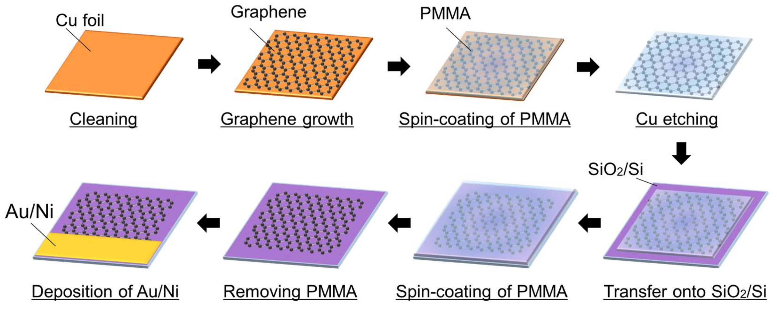
2.2. Fabrication of Graphene Electrode

Figure 1 shows the fabrication process of graphene electrodes. A graphene film was grown by low-pressure CVD on a 30-µm-thick polycrystalline copper foil (60 × 30 mm2) in a conventional quartz tube furnace by using CH4 and H2 gases. Prior to CVD growth, the copper foil was cleaned with ultrasonic waves by using DI water, ethanol, and acetone. Before the growth of graphene, the copper foil was heated under H2 flow (20 sccm) with a pressure of 650 Pa at 1000 °C for 30 min in order to remove the surface natural oxide layer. The growth was carried out for 30 min under CH4 (2 sccm) and H2 (20 sccm) flow at 1000 °C with a total pressure of 680 Pa. After the CVD growth, the graphene-deposited copper foil was divided by cutting into eight samples (15 × 15 mm2). The graphene films on the copper foils were then transferred onto chemically inert SiO2/Si substrates, with 300-nm-thick SiO2 layers on the top, via the PMMA assisted transfer method as follows [19]. The PMMA was dissolved in ethyl lactate at a concentration of 4 wt%. The PMMA layers were coated on graphene/copper foils at 2000 rpm for 1 min and cured at 180 °C for 1 min. A graphene layer that grew on the backside of the copper foil was eliminated by oxygen plasma treatment at 20 W for 30 s using a compact etcher, the FA-1 (SAMCO Inc.). The samples were immersed in a 0.5 M Fe(NO3)3 solution for 5 h to eth the copper foils away. After the etching, the PMMA/graphene layers were rinsed three times with floating on DI water for 1 h and transferred onto SiO2/Si substrates. After drying the samples, a second PMMA coating step was performed, and the samples were left at room temperature for 30 min [20]. After that, the PMMA layers were removed by immersing the samples in acetone for a night. Finally, nickel (10 nm) and gold (50 nm) layers were successively evaporated at the side position of the transferred graphene film as the electrical contact for the electrochemical measurements. Our typical CVD-grown graphene prepared in this process has a sheet resistance in the ranges of 700–1200 Ω/sq [21].

2.3. Characterizaiton of Graphene Electrode

Raman measurements were performed by using an inVia Reflex (Renishaw, Wootton-under-Edge, UK). Electrochemical measurements were performed with a three electrode system, including a graphene film on a SiO2/Si substrate as a working electrode (WE), a platinum wire spiral as a counter electrode (CE), and Ag/AgCl as a reference electrode (RE) by using the polytetrafluoroethylene housing unit cell with a fluorine rubber O-ring defining the measurement area (0.13 cm2), as shown in Figure 2. Cyclic voltammetry (CV) and electrochemical impedance spectroscopy (EIS) measurements were performed by using an Autolab PGSTAT204 potentiostat/galvanostat system equipped with an impedance analyzer FRA32M (Metrohm, Utrecht, The Netherlands). A series of electrochemical measurements was performed without dismounting the graphene electrode from the electrochemical cell because the graphene film may be damaged when detaching the O-ring. We used single sample for each of a series of measurements and in other words, three graphene electrodes were used for the whole experiment in this paper. On the other hand, we conducted similar experiment using other graphene electrodes to verify the findings.

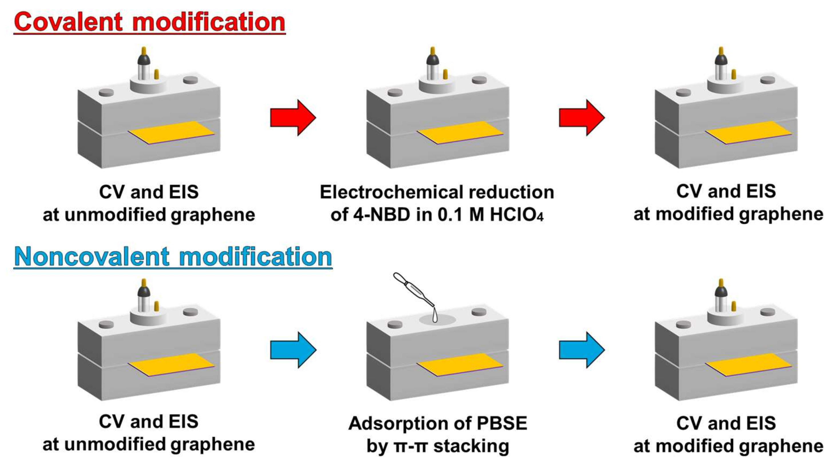
2.4. Surface Modification of Gaphene Eectrode

Covalent and noncovalent modifications were performed using a couple of films of monolayer CVD-grown graphene prepared in the same CVD batch. The EIS and CV measurements were carried out before and after modifications. Their schemes are shown in Figure 3. The covalent modification of the graphene surface was performed by grafting of nitrophenyl groups with electrochemical reduction of diazonium salt. Potential cycling was performed in a 0.1 M HClO4 solution containing 1 mM 4-NBD between 0.6 V and −0.4 V by using the graphene electrode with a scan rate of 50 mV/s [22]. The electrochemical modification was performed by using the electrochemical cell shown in Figure 2. A series of electrochemical measurements and modification was performed without dismounting the graphene electrode from the electrochemical cell.
PBSE was used for the noncovalent modification on the graphene surface. PBSE is a typical linker molecule for immobilizing biomolecules onto carbon-based materials as its pyrenyl group interacts with six-membered ring structures of graphene sheets by π–π stacking [23,24]. The noncovalent modification on the graphene surface was also conducted by using the electrochemical cell. After the initial EIS and CV measurements, the graphene electrode mounted electrochemical cell was filled with a methanol solution containing 1 mM PBSE and left for the adsorption for 3 hours at room temperature. Thereafter, the graphene surface was washed with methanol and DI water, and then characterized by EIS and CV measurements again.

3. Results and Discussion

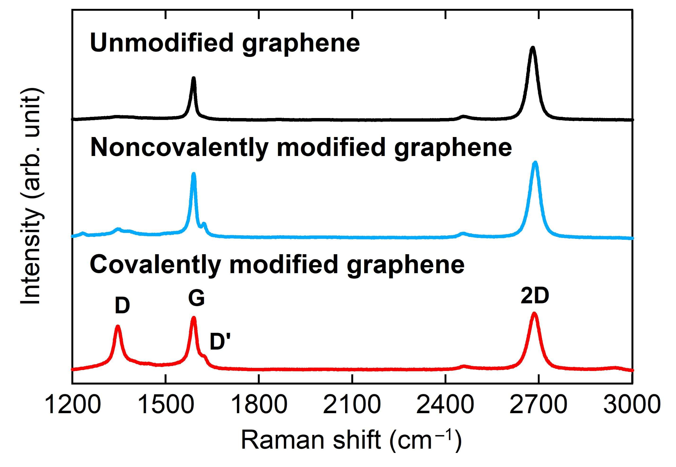
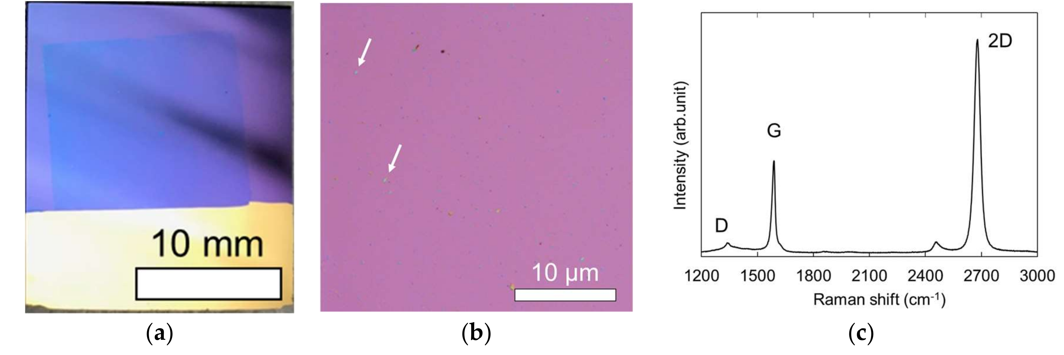
3.1. Characterizaiton of Graphene Electrode

Figure 4a shows a macroscopic image of transferred graphene film (15 × 15 mm2) on a SiO2/Si substrate. Monolayer graphene films on SiO2/Si substrates become visible owing to light interference in 300-nm-thick SiO2 layers [25]. This confirmed that the transferred CVD-grown graphene films were macroscopically uniform. Figure 4b shows an optical micrograph of the transferred graphene film. Although it shows a slight amount of PMMA residues, uniform surface with no structural tears were observed. Figure 4c shows the typical Raman spectrum of the graphene films on the SiO2/Si substrate. The 2D (2678 cm−1) and G (1587 cm−1) peaks, which are characteristic features of graphene [26], were clearly observed in the spectrum. The full width at half maximum (FWHM) of the 2D peak was 38 cm−1, and the intensity ratio I2D/IG was 2.32. The 2D peak can be fitted by a single Lorentzian, which is the characteristic feature of monolayer graphene. Although a slight D peak at ~1350 cm−1, which represents disordered carbon, was observed, the spectrum indicates that the crystalline quality of the graphene film is still high.

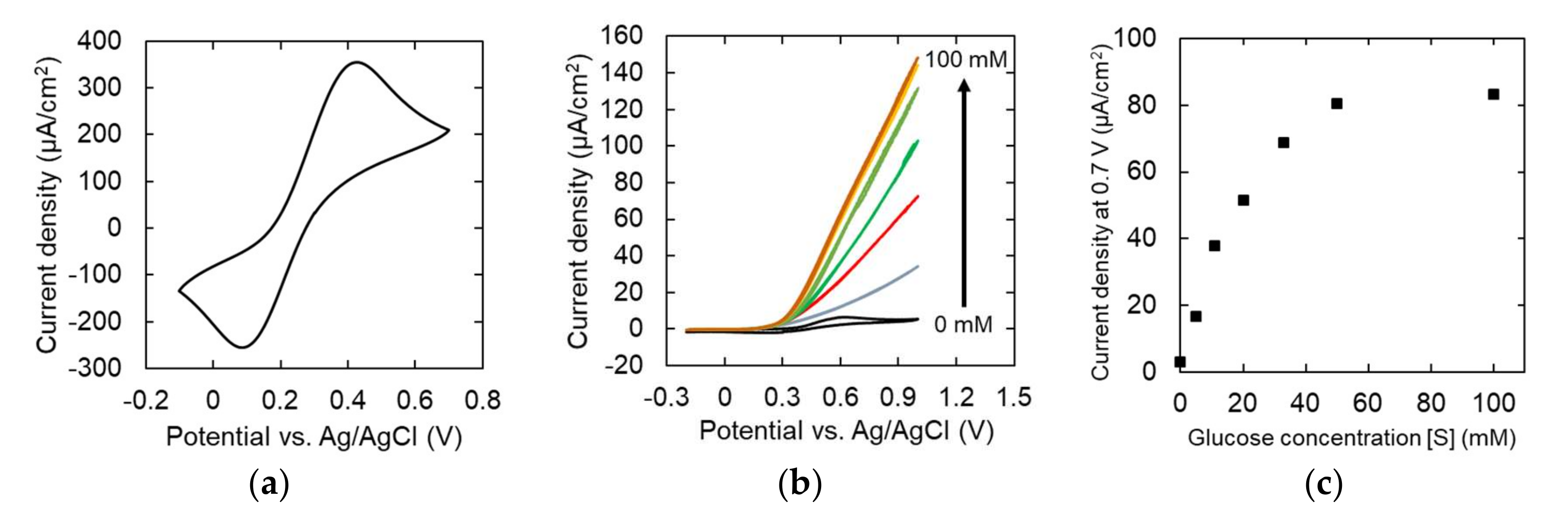
3.2. Electrochemical Behavior of Monolayer Gaphene Eectrode

First, we performed an enzyme electrode reaction via a mediator at an individual monolayer graphene electrode on an insulating substrate so as to confirm whether this one-atom-thick material graphene could be used as a platform for investigating the electrochemical properties of a biomolecule/electrode interface. Figure 5a shows cyclic voltammograms (CVs) of a monolayer graphene electrode in a 0.2 M PBS containing 10 mM FcDA as a redox-probe. It exhibited a pair of stable and well-defined anodic and cathodic peaks at 0.43 V and 0.09 V (vs. Ag/AgCl). These redox peak potentials agreed with the reported potentials of the oxidation and reduction of the ferrocene derivative on the carbon electrode [27]. The biocatalytic activation of the GOx utilizing FcDA as a mediator was electrochemically characterized by analyzing the reaction of the glucose oxidation. Figure 5b presents CVs of the monolayer graphene electrode in 0.2 M PBS containing 10 mM FcDA, 10 µM GOx, and 0–100 mM glucose. A notable increase in the biocatalytic current was observed at E > 0.2 V, which corresponds to the oxidation potential of FcDA. The oxidation current increased as the glucose concentration was elevated. Figure 5c shows plots of the biocatalytic current of the CV at a potential of 0.7 V versus glucose concentration. The biocatalytic current exhibited a plateau of 83 µA/cm2 at concentrations higher than 50 mM. This behavior represents Michaelis–Menten kinetics given below:
I 0 = I max × S K M + S
where I0, Imax, [S], and K′M represent the current response, maximum current density, glucose concentration, and apparent Michaelis constant of a monolayer graphene electrode, respectively. Imax and K′M were determined to be 83.2 μA/cm2 and 35.8 mM, respectively. These results indicate that GOx near the surface of the graphene maintained catalytic enzyme activity and also that electron transfer between the GOx and graphene was mediated by FcDA. Thus, the enzyme electrode reaction could be observed even with monolayer graphene having a thickness of only one atomic layer.

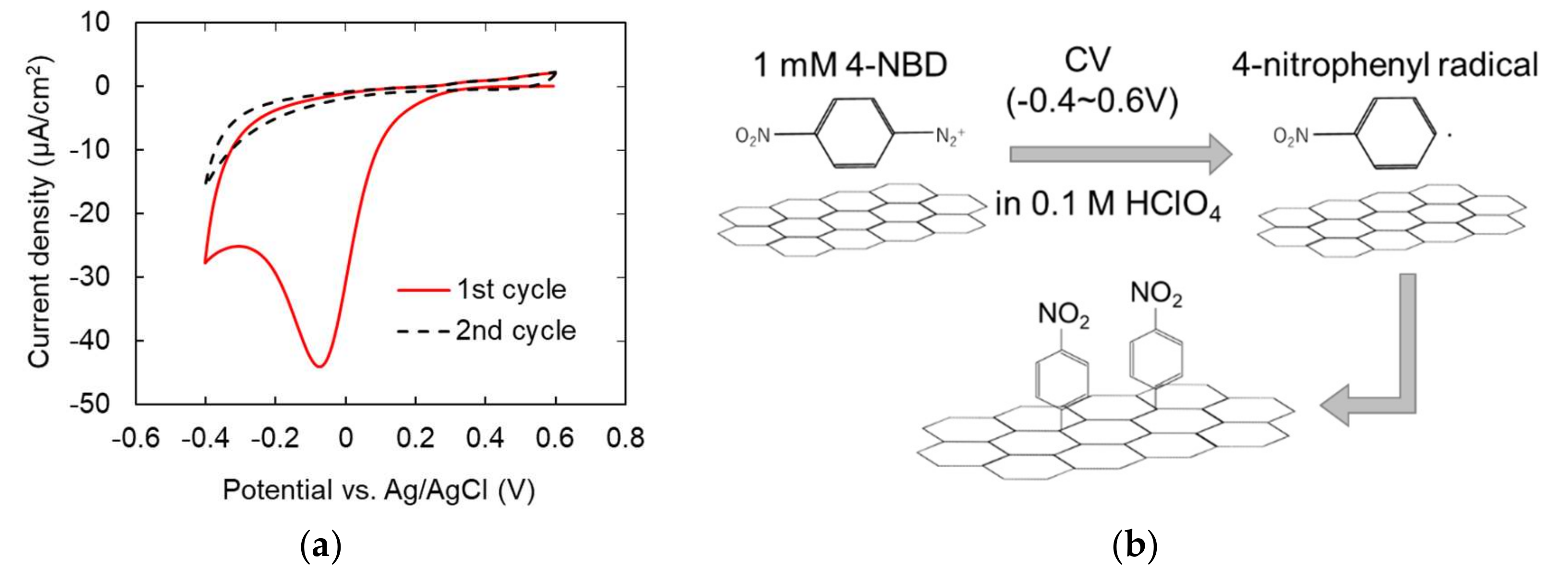
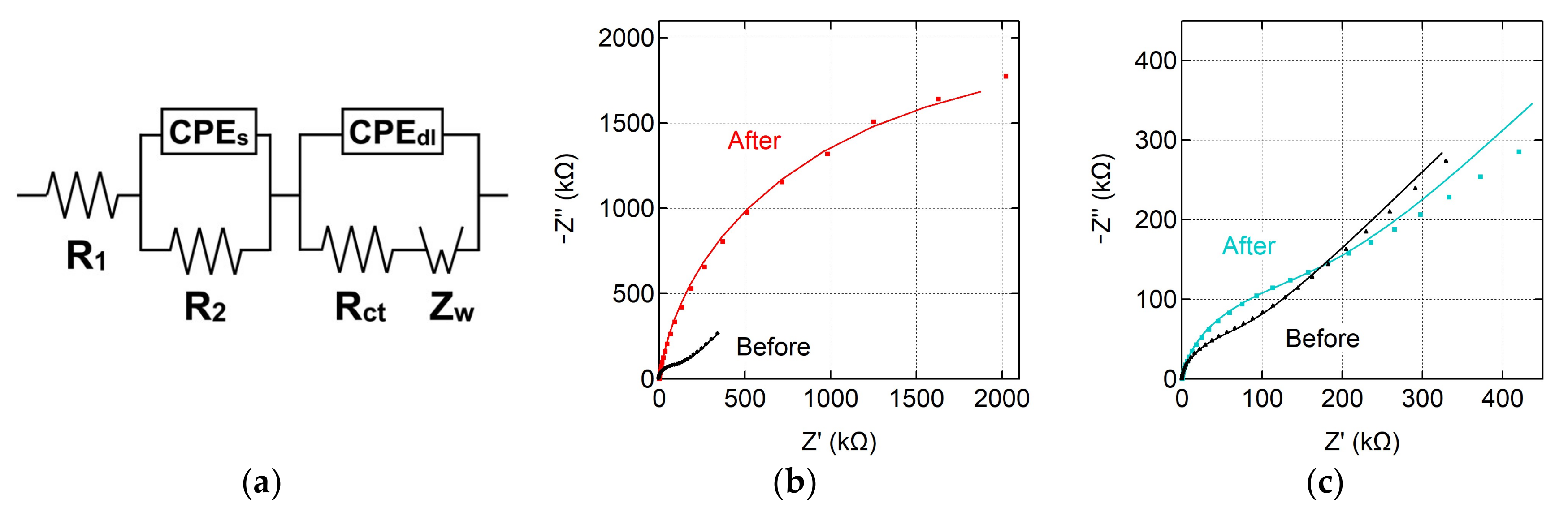
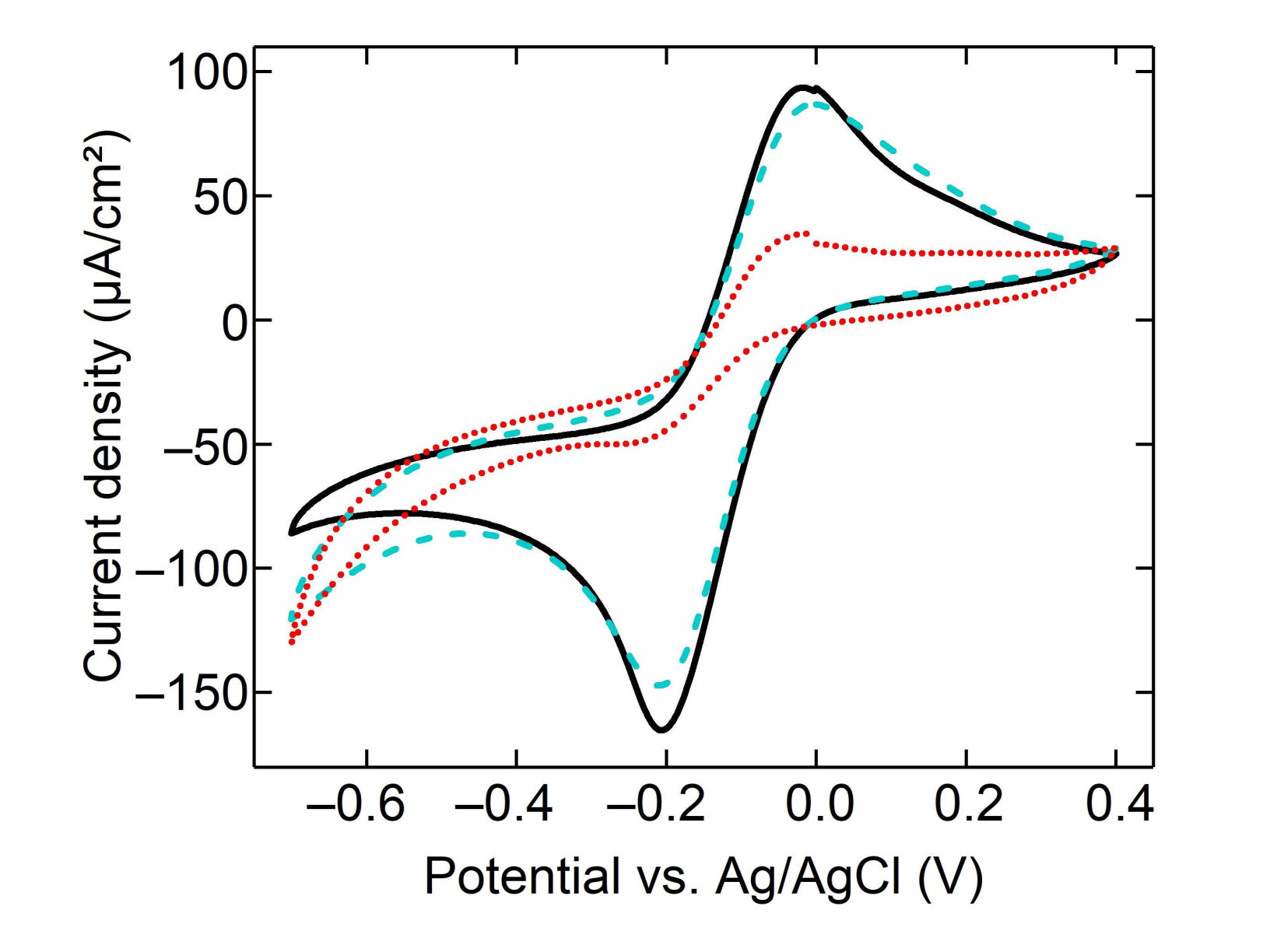
3.3. Characterization of Modified Graphene Electrodes

The monolayer graphene electrode surfaces were modified by using two molecular modification methods, the noncovalent and covalent modifications, and then characterized by Raman spectroscopy, electrochemical impedance measurements, and cyclic voltammetry. Figure 6a shows the CVs done using an aqueous solution containing 1 mM 4-NBD and 0.1 M HClO4 for the covalent modification of the graphene electrode. The first cycle showed a broad irreversible peak around −30 mV vs. Ag/AgCl, which was assigned to the reduction of the 4-NBD cations to form the corresponding aryl radicals. The second cycle was featureless, which suggests that the surface was blocked by the products that formed during the first cycle [22]. Figure 6b shows the reported mechanism of covalent modification to the graphene surface caused by the CVs [28]. Covalent modification of graphene from radicals produced from diazonium reagents is the most common method of covalent modification. The mechanism involves the transfer of a delocalized electron from the carbon surface to a diazonium cation and results in the release of a N2 molecule and the formation of a radical species. Subsequently, the radical species attacks a sp2 hybridized carbon lattice atom on the surface forming a covalent bond and converting it into sp3 hybridized carbon [28,29]. For the noncovalent modification, π–π stacking between six-membered ring of graphene sheets and pyrenyl groups of PBSE was utilized.
Figure 7 shows Raman spectra of the unmodified, covalently modified and noncovalently modified graphene films on the SiO2/Si substrates. For the unmodified graphene, the 2D (2681 cm−1) and G (1590 cm−1) peaks, both characteristic features of graphene [25,26,30], were clearly observed in the spectrum, similar to the spectrum shown in Figure 4c. For the noncovalent modified graphene, the 2D (2688 cm−1) peak shows slight upshift compared to the unmodified graphene, while the G peak (1590 cm−1) is shown at similar wavenumber. In addition, the appearance of a D’ peak (1622 cm−1) was observed, which is mainly caused by defects generated via an intravallery double-resonance process [31], and it was also observed in the Raman spectra of other PBSE-modified graphene [32]. Thus, the change of the Raman spectrum suggests the attachment of the pyrenyl groups onto the graphene surface. The covalent modified graphene electrode was also confirmed to be modified with the nitrophenyl groups due to emergence of the D’ peak (1620 cm−1) in the Raman spectrum. The covalently modified graphene also show slight upshift of the 2D peak (2686 cm−1) and no shift of the G peak (1590 cm−1). However, the appearance of a strong D (1346 cm−1) peak due to defects in the graphene was observed in the covalently modified graphene. The activation of this strong D peak is attributed to breaking of the C-C sp2 bonds after the grafting of nitrophenyl groups on the graphene surface [33]. Here, the intensity ratio I2D/IG for the unmodified, noncovalently modified and covalently modified graphene were 1.78, 1.21 and 1.12, respectively. The decrease in I2D/IG and the upshift in 2D peak that were observed after both modifications indicate the p-doping effect on graphene. These observations of 2D peak shift are in agreement with previous experimental results on PBSE-modified [32] and nitrophenyl-modified graphene [13]. Thus, these Raman spectra confirmed that the noncovalently and covalently modified graphene electrodes were prepared.
The EIS measurements were performed to observe changes by the molecular modifications in the electron transport properties inside the graphene electrode film and in electron transfer properties across the electrode/electrolyte interface. The impedance spectra were recorded in the frequency range of 100 kHz down to 0.1 Hz with 10 points per decade, at open circuit potential, 0.3 V, using a 10 mV amplitude sinusoidal voltage in 0.1 M PBS containing 1 mM FcDA. We assumed an equivalent circuit based on a Randles-type equivalent circuit, as shown in Figure 8a, including a series resistance, R1, constant phase element associated to the graphene/SiO2/Si structure, CPEs, electrical transport resistance parallel to the CPEs, R2, charge transfer resistance, Rct, constant phase element associated to double layer capacitance, CPEdl, and Warburg element, Zw. These parameters are determined from a curve fitting of a Nyquist plot. Here, we assumed that the monolayer graphene electrodes have larger internal resistance than the resistance of solution used in this measurement condition, and that CPEs is parallel to a part of the electrical transport resistance in the graphene films. Therefore, R1 was regarded as the sum of the solution resistance and a part of the electrode internal resistance and the electrode internal resistance was considered to be included also in R2. Accordingly, the sums of the R1 and R2 were compared before and after the modifications to estimate the variations in electrode internal resistance by the molecular modification because the solution resistance should be almost constant in the same measurement conditions. The Rct values for the electrochemical reaction of FcDA can be directly measured as a semicircle diameter. Figure 8b,c show the Nyquist plots for the graphene electrodes before and after the covalent and noncovalent modifications, respectively. The fitting EIS parameters are listed in Table 1. The black curves in both Nyquist plots show spectra of the unmodified graphene electrodes. The variations in the fitting parameters between both unmodified graphene electrodes are attributed to the errors resulting from the fabrication process including the transferred position of graphene sheet, PMMA residues and microscopic cracks of the SiO2 layer. In the Nyquist plots for the covalent modification, the Rct and the sum of R1 and R2 before modification were determined to be 104 kΩ and 880 Ω, respectively, by equivalent circuit fitting in the impedance spectra. After the covalent modification, the Nyquist semicircle was significantly enlarged, indicating an increase in Rct. The Rct was determined to be 2.75 MΩ, which is approximately 25-fold higher than before modification, while the sum of R1 and R2 was 907 Ω, which is almost maintained. The significant increase in Rct was possibly due to the covalently modified nitro phenyl groups blocking the reaction site of the graphene. This result is consistent with the reduction current in the second cycle for covalent modification being significantly inhibited, as shown in Figure 6a. In comparison, there was no significant change in the sum of R1 and R2 corresponding to the variation of electrode internal resistance. It suggests that the covalent modification partly broke the C-C sp2 bonds and most of the remaining π-conjugated network still worked. For the noncovalent modification, the Rct and the sum of R1 and R2 before the modification were determined to be 67 kΩ and 721 Ω, respectively, and after the modification, these values were changed to be 158 kΩ and 658 Ω, respectively. The decrease in the sum of R1 and R2 after the noncovalent modification indicates the resistance for electric transport in the graphene film decreased attributed to the p-doping effect of PBSE. On the other hand, the slight increase in Rct after the modification is ascribed to butanoic acid, the molecular chains of PBSE, which may interfere the approach of the FcDA to the graphene surface. Nevertheless, the Rct value for the noncovalent modified graphene was much lower than that of the covalent modified graphene and comparable to those before the surface modifications. Thus, noncovalent bonds using π–π stacking allow molecular modifications without degrading the resistance properties of the graphene.
Subsequently, to confirm that the above change in electrochemical properties is observed for the other redox system, an evaluation was performed by cyclic voltammetry using [Ru(NH3)6]Cl3, which is a widely used redox for characterizing electrodes. Figure 9 shows CVs for 1 mM [Ru(NH3)6]Cl3 in 0.1 M KCl at the unmodified and covalently and noncovalently modified graphene electrodes at a scan rate of 100 mV/s. Well-defined oxidation and reduction peaks were observed at the unmodified and noncovalently modified graphene electrodes. The peak-to-peak separation ΔEp at the unmodified graphene electrode was 190 mV. We estimated k0 from the measured ΔEp as 1.1 × 10⁻³ cm/s by using the Nicholson’s method [34,35], which corresponds to a quasi-reversible system (10−2 > k0 > 10−4). Also, the ΔEp at the noncovalently modified graphene electrode was 208 mV, and k0 was estimated to be 8.1 × 10⁻⁴ cm/s from the measured ΔEp. This also corresponds to a quasi-reversible system, and there was no significant change compared with before modification. In comparison, significant decrease in current density and no reduction peak were observed for the covalently modified graphene electrode. These electrochemical behaviors are consistent to results of the EIS measurements. Therefore, these results suggest that covalent modification for an individual graphene sheet can significantly affect charge transfer between graphene and electrolyte, while noncovalent modification shows little degradation in electrochemical properties despite the one-atom-thick electrode. Such trends in electrochemical properties by both molecular modifications were confirmed by using the other graphene electrodes although there are differences of degree.

4. Conclusions

In summary, we investigated the electrochemical properties of graphene electrodes before and after molecular modification. Nitrophenyl groups were immobilized via covalent bonding on a graphene electrode by using the electrochemical reduction of 4-NBD salt. Also, PBSE was noncovalently modified on a graphene electrode by a pyrenyl group. Furthermore, the properties of graphene before and after molecular modification were characterized by using Raman spectroscopy, electrochemical impedance spectroscopy, and cyclic voltammetry. Noncovalent modification with a pyrenyl group can be performed nearly without degrading the electrochemical properties of graphene. However, the covalent modification by using the electrochemical reduction of 4-NBD salt introduced a lot of defects in the graphene, and the surface-grafted nitrophenyl groups suppressed the charge transfer between the graphene and the electrolytes. Therefore, these results suggest that the noncovalently modified graphene electrode retains the excellent electrochemical properties of graphene. Our results demonstrate that CVD-grown monolayer graphene can be a platform for investigating the interface of molecule and carbon-based materials.

Author Contributions

K.M., T.W. and S.K. designed the experiments. K.M. carried out the experiments. K.M. and T.W. analyzed the data, and wrote and revised the manuscript. All authors discussed and commented on the manuscript. All authors have read and agreed to the published version of the manuscript.

Funding

This work was partly supported by a Grant-in-Aid for Scientific Research (17K05043 and 19K05218) from the Japan Society for the Promotion of Science, by the Nippon Sheet Glass Foundation for Materials Science and Engineering, and by an Aoyama Gakuin University research grant, “Early Eagle.”

Acknowledgments

The Raman measurements in this work were supported by the Center for Instrumental Analysis, College of Science and Engineering, Aoyama Gakuin University.

Conflicts of Interest

The authors declare no conflicts of interest associated with this manuscript.

References

  1. Larminie, J.; Dicks, A. Fuel Cell Systems Explained; John Wiley & Sons, Ltd.: England, UK, 2003; ISBN 9781118878330. [Google Scholar]
  2. Cao, L. Immobilised enzymes: Science or art? Curr. Opin. Chem. Biol. 2005, 9, 217–226. [Google Scholar] [CrossRef]
  3. Boland, S.; Jenkins, P.; Kavanagh, P.; Leech, D. Biocatalytic fuel cells: A comparison of surface pre-treatments for anchoring biocatalytic redox films on electrode surfaces. J. Electroanal. Chem. 2009, 626, 111–115. [Google Scholar] [CrossRef]
  4. Cracknell, J.A.; Vincent, K.A.; Armstrong, F.A. Enzymes as working or inspirational electrocatalysts for fuel cells and electrolysis. Chem. Rev. 2008, 108, 2439–2461. [Google Scholar] [CrossRef] [PubMed]
  5. Barton, S.C.; Gallaway, J.; Atanassov, P. Enzymatic biofuel cells for implantable and microscale devices. Chem. Rev. 2004, 104, 4867–4886. [Google Scholar] [CrossRef] [PubMed]
  6. Gallaway, J.W.; Calabrese Barton, S.A. Effect of redox polymer synthesis on the performance of a mediated laccase oxygen cathode. J. Electroanal. Chem. 2009, 626, 149–155. [Google Scholar] [CrossRef]
  7. Shim, J.; Kim, G.Y.; Moon, S.H. Covalent co-immobilization of glucose oxidase and ferrocenedicarboxylic acid for an enzymatic biofuel cell. J. Electroanal. Chem. 2011, 653, 14–20. [Google Scholar] [CrossRef]
  8. Halámková, L.; Halámek, J.; Bocharova, V.; Szczupak, A.; Alfonta, L.; Katz, E. Implanted biofuel cell operating in a living snail. J. Am. Chem. Soc. 2012, 134, 5040–5043. [Google Scholar] [CrossRef]
  9. Hoshi, K.; Muramatsu, K.; Sumi, H.; Nishioka, Y. Graphene-coated carbon fiber cloth for flexible electrodes of glucose fuel cells. Jpn. J. Appl. Phys. 2016, 55, 02BE05. [Google Scholar] [CrossRef]
  10. Liu, C.; Alwarappan, S.; Chen, Z.; Kong, X.; Li, C.Z. Membraneless enzymatic biofuel cells based on graphene nanosheets. Biosens. Bioelectron. 2010, 25, 1829–1833. [Google Scholar] [CrossRef]
  11. Zebda, A.; Gondran, C.; Le Goff, A.; Holzinger, M.; Cinquin, P.; Cosnier, S. Mediatorless high-power glucose biofuel cells based on compressed carbon nanotube-enzyme electrodes. Nat. Commun. 2011, 2, 370. [Google Scholar] [CrossRef] [Green Version]
  12. Holzinger, M.; Le Goff, A.; Cosnier, S. Carbon nanotube/enzyme biofuel cells. Electrochim. Acta 2012, 82, 179–190. [Google Scholar] [CrossRef]
  13. Das, B.; Voggu, R.; Rout, C.S.; Rao, C.N.R. Changes in the electronic structure and properties of graphene induced by molecular charge-transfer. Chem. Commun. 2008, 44, 5155–5157. [Google Scholar] [CrossRef] [PubMed] [Green Version]
  14. Zhu, C.; Du, D.; Lin, Y. Graphene-like 2D nanomaterial-based biointerfaces for biosensing applications. Biosens. Bioelectron. 2017, 89, 43–55. [Google Scholar] [CrossRef]
  15. Reina, A.; Jia, X.; Ho, J.; Nezich, D.; Son, H.; Bulovic, V.; Dresselhaus, M.S.; Jing, K. Large area, few-layer graphene films on arbitrary substrates by chemical vapor deposition. Nano Lett. 2009, 9, 30–35. [Google Scholar] [CrossRef] [PubMed]
  16. Geim AK, N.K. The rise of graphene. Chem. Rev. 2017, 114, E9793–E9801. [Google Scholar]
  17. Ogawa, Y.; Komatsu, K.; Kawahara, K.; Tsuji, M.; Tsukagoshi, K.; Ago, H. Structure and transport properties of the interface between CVD-grown graphene domains. Nanoscale 2014, 6, 7288–7294. [Google Scholar] [CrossRef]
  18. Novoselov, K.S. Electric Field Effect in Atomically Thin Carbon Films. Science 2004, 306, 666–669. [Google Scholar] [CrossRef] [PubMed] [Green Version]
  19. Kang, J.; Shin, D.; Bae, S.; Hong, B.H. Graphene transfer: Key for applications. Nanoscale 2012, 4, 5527–5537. [Google Scholar] [CrossRef]
  20. Li, X.; Zhu, Y.; Cai, W.; Borysiak, M.; Han, B.; Chen, D.; Piner, R.D.; Colombo, L.; Ruoff, R.S. Transfer of Large-Area Graphene Films for High-Performance Transparent Conductive Electrodes. Nano Lett. 2009, 9, 4359–4363. [Google Scholar] [CrossRef]
  21. Kosuga, S.; Suga, K.; Suga, R.; Watanabe, T.; Hashimoto, O.; Koh, S. Radiation properties of graphene-based optically transparent dipole antenna. Microw. Opt. Technol. Lett. 2018, 60, 2992–2998. [Google Scholar] [CrossRef]
  22. Greenwood, J.; Phan, T.H.; Fujita, Y.; Li, Z.; Ivasenko, O.; Vanderlinden, W.; Van Gorp, H.; Frederickx, W.; Lu, G.; Tahara, K.; et al. Covalent modification of graphene and graphite using diazonium chemistry: Tunable grafting and nanomanipulation. ACS Nano 2015, 9, 5520–5535. [Google Scholar] [CrossRef] [PubMed] [Green Version]
  23. Chen, R.J.; Zhang, Y.; Wang, D.; Dai, H. Noncovalent Sidewall Functionalization of Single-Walled Carbon Nanotubes for Protein Immobilization. J. Am. Chem. Soc. 2001, 123, 3838–3839. [Google Scholar] [CrossRef] [PubMed]
  24. Ebrish, M.A.; Olson, E.J.; Koester, S.J. Effect of noncovalent basal plane functionalization on the quantum capacitance in graphene. ACS Appl. Mater. Interfaces 2014, 6, 10296–10303. [Google Scholar] [CrossRef]
  25. Blake, P.; Hill, E.W.; Castro Neto, A.H.; Novoselov, K.S.; Jiang, D.; Yang, R.; Booth, T.J.; Geim, A.K. Making graphene visible. Appl. Phys. Lett. 2007, 91, 063124. [Google Scholar] [CrossRef] [Green Version]
  26. Ferrari, A.C.; Basko, D.M. Raman spectroscopy as a versatile tool for studying the properties of graphene. Nat. Nanotechnol. 2013, 8, 235–246. [Google Scholar] [CrossRef] [PubMed] [Green Version]
  27. Rabti, A.; Raouafi, N.; Merkoçi, A. Bio(Sensing) devices based on ferrocene–functionalized graphene and carbon nanotubes. Carbon N. Y. 2016, 108, 481–514. [Google Scholar] [CrossRef]
  28. Kirkman, P.M.; Güell, A.G.; Cuharuc, A.S.; Unwin, P.R. Spatial and temporal control of the diazonium modification of sp 2 carbon surfaces. J. Am. Chem. Soc. 2014, 136, 36–39. [Google Scholar] [CrossRef]
  29. Baranton, S.; Bélanger, D. Electrochemical derivatization of carbon surface by reduction of in situ generated diazonium cations. J. Phys. Chem. B 2005, 109, 24401–24410. [Google Scholar] [CrossRef]
  30. Ferrari, A.C.; Meyer, J.C.; Scardaci, V.; Casiraghi, C.; Lazzeri, M.; Mauri, F.; Piscanec, S.; Jiang, D.; Novoselov, K.S.; Roth, S.; et al. Raman spectrum of graphene and graphene layers. Phys. Rev. Lett. 2006, 97, 187401. [Google Scholar] [CrossRef] [Green Version]
  31. Malard, L.M.; Pimenta, M.A.; Dresselhaus, G.; Dresselhaus, M.S. Raman spectroscopy in graphene. Phys. Rep. 2009, 473, 51–87. [Google Scholar] [CrossRef]
  32. Wu, G.; Tang, X.; Meyyappan, M.; Lai, K.W.C. Doping effects of surface functionalization on graphene with aromatic molecule and organic solvents. Appl. Surf. Sci. 2017, 425, 713–721. [Google Scholar] [CrossRef]
  33. Sharma, R.; Baik, J.H.; Perera, C.J.; Strano, M.S. Anomalously large reactivity of single graphene layers and edges toward electron transfer chemistries. Nano Lett. 2010, 10, 398–405. [Google Scholar] [CrossRef] [PubMed]
  34. Nicholson, R.S. Theory and Application of Cyclic Voltammetry for Measurement of Electrode Reaction Kinetics. Anal. Chem. 1965, 37, 1351–1355. [Google Scholar] [CrossRef]
  35. Lavagnini, I.; Antiochia, R.; Magno, F. An extended method for the practical evaluation of the standard rate constant from cyclic voltammetric data. Electroanalysis 2004, 16, 505–506. [Google Scholar] [CrossRef]
Figure 1. The fabrication process of the graphene electrodes.
Crystals 10 00241 g001
Figure 2. Electrochemical cell set-up used for all electrochemical measurements.
Crystals 10 00241 g002
Figure 3. The measurement and modification schemes for evaluating influences of the covalent and noncovalent modifications on electrochemical properties of the graphene electrodes. The graphene electrodes were not dismounted form the cells in the whole process.
Crystals 10 00241 g003
Figure 4. Characterization of the chemical vapor deposition (CVD)-grown graphene film on SiO2/Si substrate. (a) Optical image after deposition of the Au /Ni (50 nm/10 nm). (b) Optical micrograph. Arrows indicate poly-methyl methacrylate (PMMA) residues. (c) Raman spectrum.
Crystals 10 00241 g004
Figure 5. Cyclic voltammogramss recorded at the chemical vapor deposition (CVD)-grown graphene on SiO2/Si substrate for 10 mM 1,1-ferrocenedicarboxylic acid in (a) the absence and (b) presence of glucose and 5–100 mM glucose and 10 µM GOx in 0.2 M phosphate buffer solution at scan rate of 50 mV/s and (c) plots of its catalytic current at E = 0.7 V vs. glucose concentration.
Crystals 10 00241 g005
Figure 6. (a) CVs during covalent modification of CVD-grown graphene using 1 mM 4-Nitrobenzenediazonium tetrafluoroborate in 0.1 M HClO4 at scan rate of 50 mV/s. (b) The schematic diagram of electrochemical covalent modification to the graphene surface.
Crystals 10 00241 g006
Figure 7. Raman spectra of unmodified, and noncovalently and covalently modified graphene on SiO2/Si substrate.
Crystals 10 00241 g007
Figure 8. (a) Equivalent circuit model used for fitting Nyquist plots. (b,c) Nyquist plots obtained at monolayer graphene electrode before and after (b) covalent and (c) noncovalent modification in 0.1 M PBS containing 1 mM FcDA. Solid lines represent fitted curves.
Crystals 10 00241 g008
Figure 9. CVs of unmodified (solid line, black), and covalently (dotted line, red) and noncovalently (dashed line, cyan) modified graphene electrodes for 1 mM hexa-ammine-ruthenium (III) in 0.1 M KCl at scan rate of 100 mV/s.
Crystals 10 00241 g009
Table 1. Fitting EIS parameters of the graphene electrodes in 0.1 M PBS containing 1 mM FcDA before and after covalent or noncovalent modification.
SampleR₁
(Ω)
R₂
(Ω)
CPEsCPEdlRct
(kΩ)
Zw
(µΩ∙s½)
χ2
Q₁
(µF∙s(n−1))
n₁Q₂
(µF∙s(n−1))
n₂
Before covalent modification1007801.25 0.69 1.90 0.99 104 3.470.003
After covalent modification1078004.64 0.61 3.18 0.92 2753 1.130.025
Before noncovalent modification2314901.45 0.75 2.00 0.97 67 3.180.010
After noncovalent modification2713870.50 0.85 2.69 0.93 158 2.660.044

