1. Introduction
In contrast to silicon, it is still a challenge to grow germanium crystals without dislocations. In specific cases, it is even not wanted to grow dislocation free, but to keep the dislocation density in a certain range. This applies for Ge used in radiation detectors, where the Ge crystal is grown in hydrogen atmosphere and not in argon because of purity reasons. In dislocation-free crystals, a hydrogen double vacancy complex will be formed with hydrogen, which leads eventually to the degradation of the detector [
1]. Dislocation multiplication is driven by thermal stresses, and thus, tuning the thermal field in the crystal is of severe importance. In the case of Czochralski growth with resistance heating, numerical results have been presented by Artemyev et al. using the software package CGsim (
http://str-soft.com/products/CGSim/) and compared with experimental results [
2]. In the case of inductive heating, which is required to grow Ge crystals for detectors, the tuning of the thermal field is much more challenging. Experimental work has been done by Wang et al. [
3]. However, no calculations have been made for these growth experiments. A global simulation for the Czochralski growth of Ge with induction heating was performed by Honarmandnia et al. [
4]. However, only the temperature field including the interface shape was computed for three distinctive growth stages. Later, they also considered thermal stress, but for a configuration with a resistance heater [
5].
In order to obtain information on dislocation density development, it is essential to simulate the entire growth process. This can be done in one run solving the time dependent heat transport equation. This approach is, e.g., realized in CGsim, but with some restrictions on the gas phase attached to the moving parts such as the crystal and melt. Furthermore, the grid is adapted in the parts of changing geometry by condensing and expanding the nodes, leading to a very dense mesh in the shrinking melt volume and a very coarse mesh in the growing crystal. Other approaches include a recalculation of the mesh in the relevant regions during the run as, e.g., that of Sabanski et al. [
6]. In this paper, we present an approach with different runs for every stage of the process. The crystal shape is preset either by the shape obtained in the experiment or an artificial one. Thus, the three phase junction (melt/gas/crystal) is defined by input, but the melt/crystal interface is calculated. We developed a script for an automatic setup of geometry and meshing for each growth stage. The calculation of the thermal and stress fields using the open source software Elmer (
https://www.csc.fi/web/elmer) is started from a script. The shape of the crystal was given previously. In this paper, we use the shapes obtained by the growth experiments to compare experimental and numerical results. However, any artificial shape can be given as an input for the computation.
2. Growth Experiment and Characterization
For the Czochralski growth of high purity Ge single crystals, a growth furnace was constructed at IKZ. Details were described elsewhere [
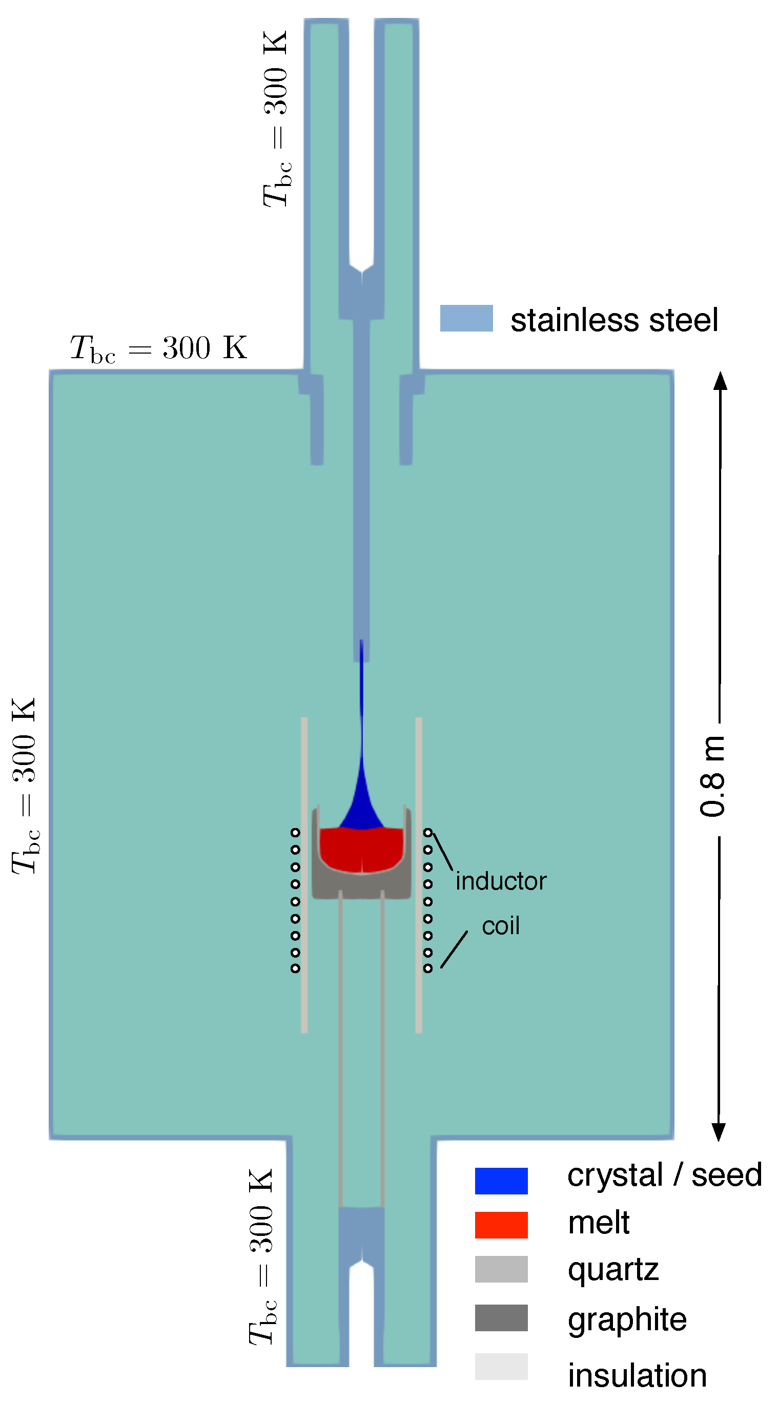
7]. A sketch for the axisymmetric calculation is presented in
Figure 1. The current setup with a quartz crucible of a 90 mm inner diameter was used to grow 2
crystals. The only graphite part in the setup was the susceptor holding the crucible. Heat was generated in the graphite part by inductive heating using a coil with 9 windings made of silver. A frequency of 80 kHz was applied. Crystals were pulled with a constant pulling velocity of
, except when the bottom cone was grown to empty the crucible. The position of the crucible was fixed during the entire process of crystal growth. As a result, the melt level was decreasing in time, resulting in a higher growth velocity of the crystal than the pulling velocity. The rotation rates of the crystal and crucible were 15 rpm and −2 rpm, respectively (counter rotation). The radius of the crystal was controlled by adapting the heating power. This was done manually. In the finishing process, the Ge melt was pulled out completely.
Two kinds of material analyses are relevant in this paper: lateral photovoltaic scanning (LPS) measurements to obtain information on the interface shape during crystal growth [
8] and etch pit density (EPD) measurements. Therefore, the crystals were cut orthogonal to the crystal growth direction for counting EPD and parallel for LPS. For EPD analysis, the polished wafers were etched to reveal the dislocations. The etch pit density was determined by manually counting the pits using a light microscope. For better comparability, all wafers were analyzed at the same positions (middle, half radius, edge) along a
and a
direction. A typical LPS setup was shown in [
9,
10]. Here, a modulated and focused laser beam exited electrons and holes, which drifted/diffused inside the sample. If a resulting doping inhomogeneity existed in the area of electron/hole movement, a potential difference would be detectable between the ohmic rim contacts by using a lock-in-technique. In the case of high charge carrier lifetime and a resulting large mean free path of charge carriers, LPS measurements are quite challenging, because the information of the local resistivity gradient is smeared out. This makes the LPS measurements for high purity Ge extremely difficult. In addition, the high intrinsic charge carrier density at room temperature sets a barrier to the measurability. In order to measure differences in local resistivity, the charge carrier concentration had to be larger than the intrinsic charge carrier density. In the current setup, the intrinsic charge carrier density was about
(at 300 K) [
11], which corresponded to a resistivity of
. The resistivity of the crystal investigated in this paper was just below this critical value (
).
3. Numerical Solution Strategy
We wanted to compute the thermal and stress fields in the crystal by an axisymmetric global calculation for a sequence of process times. This should be done automatically considering the changes in geometry and in the growth velocity of the crystal because the melt height was changing during the process. Therefore, we developed a perl script calling to Gmsh (
http://gmsh.info/) [
12] for geometry and mesh creation and afterwards to Elmer (
https://www.csc.fi/web/elmer) for the calculation. Results were analyzed using Paraview (
https://www.paraview.org/).
The calculations were performed in steps
of the crystal length. For all computations presented in this paper, we set
. Because the pulling velocity was constant, but the melt height was changing, this meant that the time for increasing the crystal length by
depended on the change in crystal volume and correspondingly in melt volume during this time step. We named the iteration step
so that the crystal had a length of
after time step
. For every
, we determined the meniscus, the melt height, and the time
required for the growth from
to
. The crystal shape was given by a data file originating either from the shape of the crystal grown or a given profile. The input data points were used for the definition of a spline function representing the shape of the crystal. Thus, we had a smooth function without abrupt changes in the boundary of the crystal. Therefore, the change in the growth angle was also continuous, which was important for the computation of the meniscus. The meniscus height
was computed by the approach of Hurle [
13]:
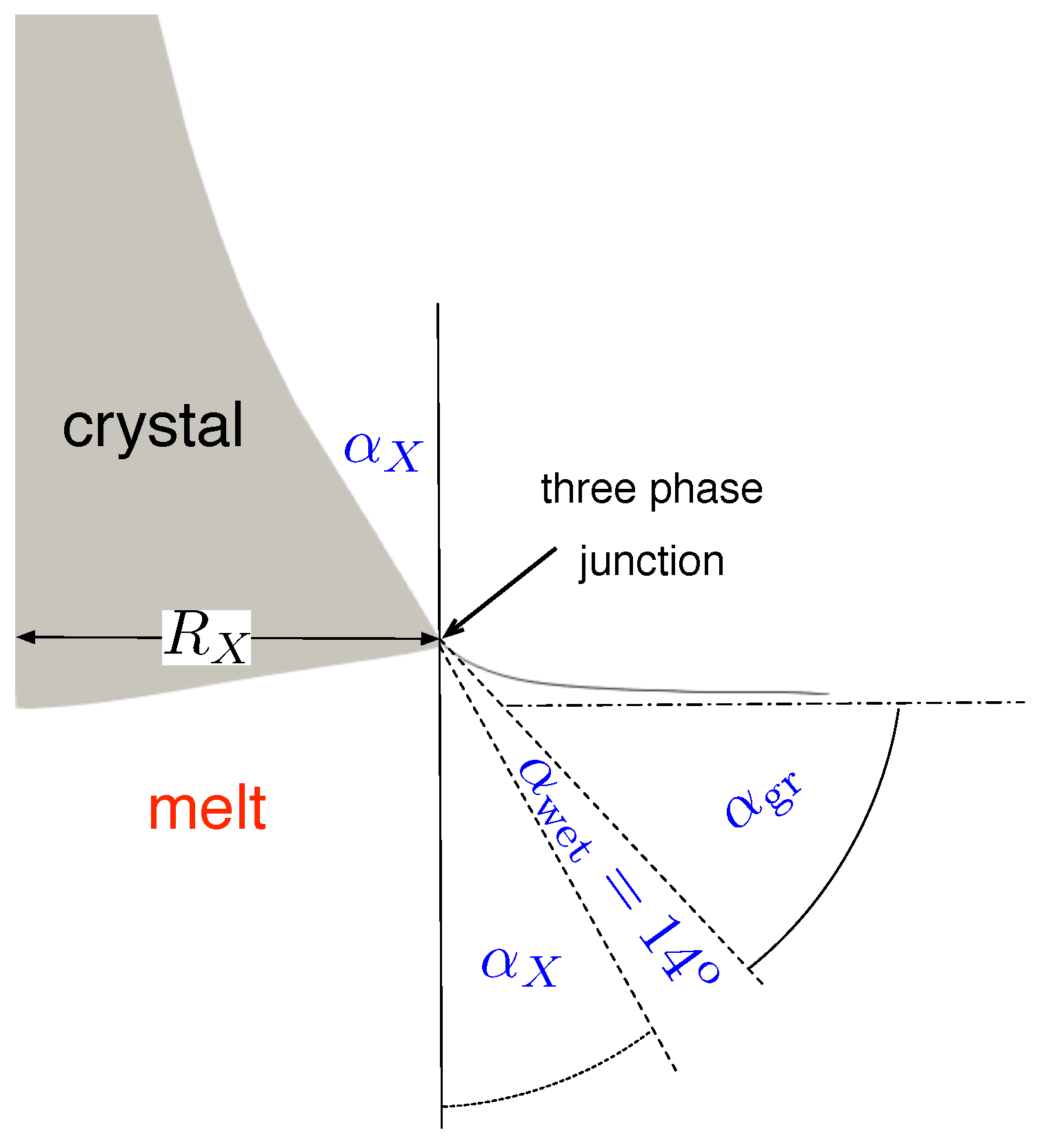
The definitions are given in
Figure 2. In particular, we have
, where
is obtained by:
is the Laplace constant, defined as
, where
is the surface tension between the melt and gas.
,
, and
g are the density of the melt, latent heat, and gravitational acceleration, respectively. In order to obtain the melt-gas interface, we computed the height
h above the melt level at the crucible. Together with the corresponding radius
r, we could computed a set of points of the melt-gas interface:
The calculation was done for values of
between
and
in steps of
. For every iteration
, the crystal volume could be computed, and thus, the required melt volume was known. The latter was used to compute the melt level at the crucible
by a simple numerical integration taking into account the melt volume beneath the crystal because of the meniscus (
). The melt volume below the meniscus itself was not taken into account. Getting
, we can now compute the time step as:
and the growth velocity by:
This velocity was used for setting the latent heat production at the interface. At this point, we would like to note that the shape of the crystal was an input for the calculations. The shape might be taken as the crystal grown in an experiment or one can preset an artificial shape. Therefore, the three phase junction (melt/gas/crystal) was defined by the input and not an object to be computed. However, one obtained the required input power as a function of time, which could be adapted in an experiment. In this paper, we used the shapes obtained in the experiments. The shape was defined via the picture of the crystal and normalized by a measured radius at a specific height.
The computation of the thermal field included heat conduction and wall-to-wall radiation, where the parts made of quartz were treated as transparent without refraction. Computations with and without gas convection both for argon and hydrogen showed that there was no significant change of the temperature field in the crystal and only little in power. In the quasi-transparent calculation, we neglected the effect of the moving crystal for the heat exchange. For the small pulling rates like or and the crystal radius of about 2, this effect was small. In the melt, we additionally computed the advective heat transport. We took into account the forced convection induced by crucible and crystal rotation, as well as the Marangoni convection at the melt/gas interface and the buoyancy convection in the volume. Melt convection was always the critical point in such calculations. In order to obtain a stationary solution, either the turbulence model or an increased viscosity could be used. For a realistic time dependent solution, a 3D calculation was required, which meant a much higher computational effort. Here, we solved the time independent Navier–Stokes equations directly without employing a turbulence model. Therefore, the viscosity used in the computation was larger by about a magnitude than the real one. In the next section, we will show that the agreement in the interface shapes during growth was good between experiment and numerical simulation, i.e., the heat transport in the melt was described well by the convection with the increased viscosity. In order to get a stable solution, we started with a viscosity of , which decreased linearly over 20 inner iterations to .
At the outer boundary of the furnace, we set a constant temperature of . We also set this temperature at the inner boundary of the inductor coil (); the coil was water cooled.
The power was adjusted by setting the melting point temperature of Ge (1210 K) at the three phase line as the target value for a feedback loop. The isoline of melting point temperature was assumed to be the melt/crystal interface. The actual interface in an iteration was moved according to the distance from the isoline of melting point temperature. The mesh in crystal and melt was adapted by solving the equation for elastic deformation. As this solver in Elmer had by default the variable displacementfor the displacement of the nodes, one had to define a new variable (e.g., displacement-stress) for the displacement used in the solver for the thermal stress.
The elastic stress due to the thermal strain
with
was computed.
is the thermal expansion coefficient, and the value is given in
Table 1. We used the temperature dependent elastic coefficients as given in
Table 2 and employed the approach of Lambropoulos [
15] for a crystal growing in the
direction:
where
H is given by
. The stress calculation was performed in the seed and crystal. Displacements in the vertical direction were set to zero at the top of the seed.
Calculations were performed on a typical desktop computer. For the crystals considered in this paper and , the complete calculation took about one day.
4. Results and Discussion
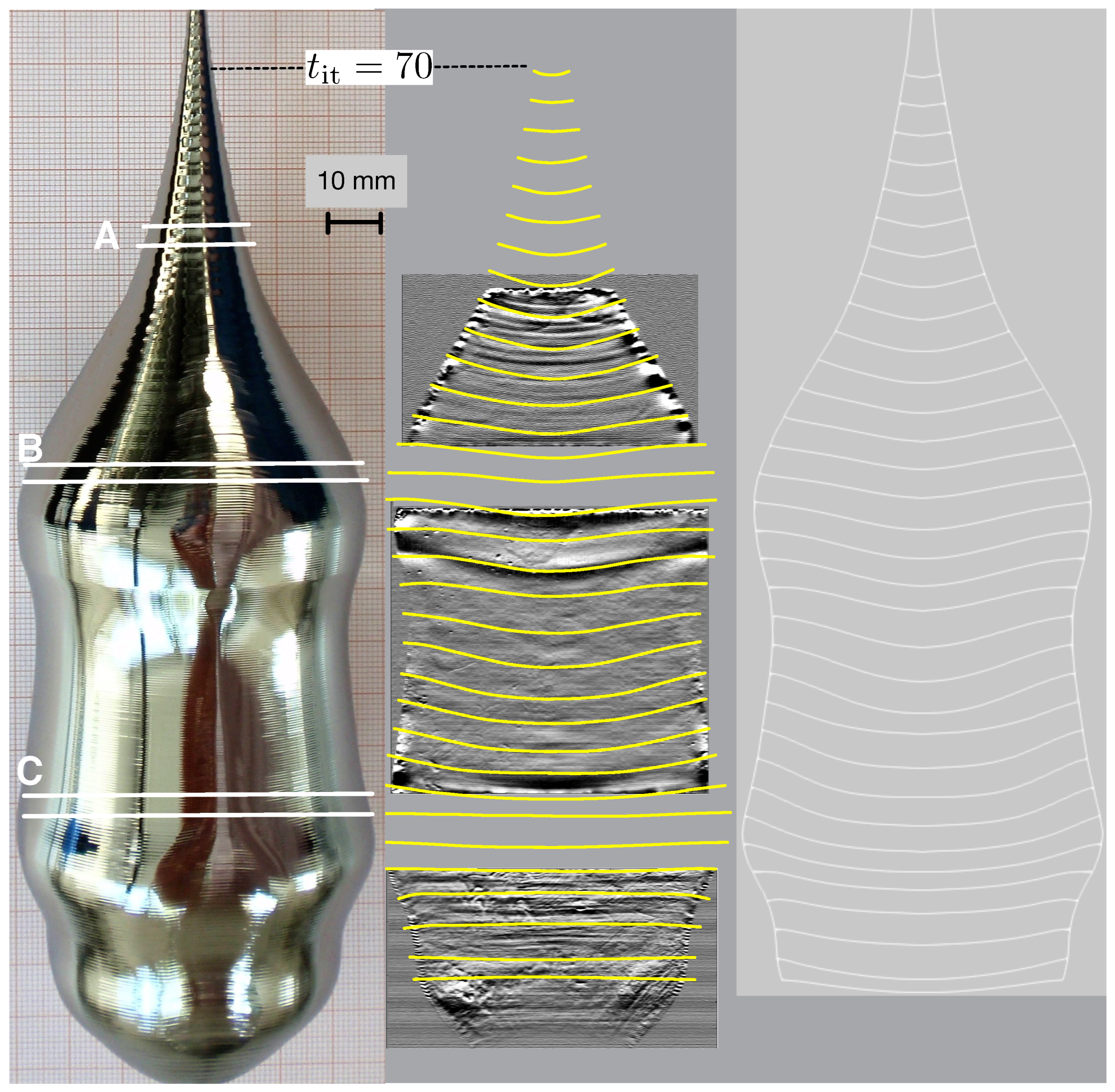
We considered two experimental runs for our numerical simulations. The examples were chosen out of a series of growth experiments for the process development, which was started with argon as the atmosphere and was later changed to hydrogen. In one case, we grew a crystal of 513 g total weight in an argon atmosphere (Case 1) and in the other one a crystal of 1530 g total weight in a hydrogen atmosphere (Case 2). Firstly, we discuss the results of Case 2. The crystal shape of the final crystal can be seen on the left hand side of
Figure 3. Three wafers were cut out of the crystal as indicated by the horizontal yellow lines. These wafers were used for the measurements of the etch pitch density (EPD), which we will discuss later. Three vertical cuts were made, in the cone, the cylindrical part, and the final cone. All three were polished chemo-mechanically and used for LPS measurements. In the middle of
Figure 3, the outcome of LPS is shown together with the computed interface lines (yellow). A good agreement can be observed over the entire growth process. Some minor differences can be seen in the middle of the shouldering. For comparison, on the right hand side, the interface lines are presented, which were obtained by running the calculation using
for computing the latent heat as was done in the standard computational scheme (
). A significant difference in the shapes can be observed in the later stages of the growth, especially towards the end. The shape of the interface is of major importance for the von Mises stress in its vicinity. In
Figure 4, the von Mises stress is shown for three different locations at the interface for the two runs with computed
and with
. The stress was always higher for
except for a short time period. Because of the high temperature, the von Mises stress in the vicinity of the interface was the most critical for the multiplication of dislocations.
We also compared the change in the required power during the process time. Please note that the experimental value was given by the electrical current and voltage in the entire circuit, whereas the numerical values were the sum of the induced heat in the graphite and melt. For comparison, we shifted the experimental values by 350 W. The comparison is shown in
Figure 5. After shouldering, the required power went down. There was some instability when reaching the cylindrical part, which was more pronounced in the numerical calculation than in the experiment. This might be because we did not perform fully transient calculations and did not take the change of the interface shape into account for the computation of
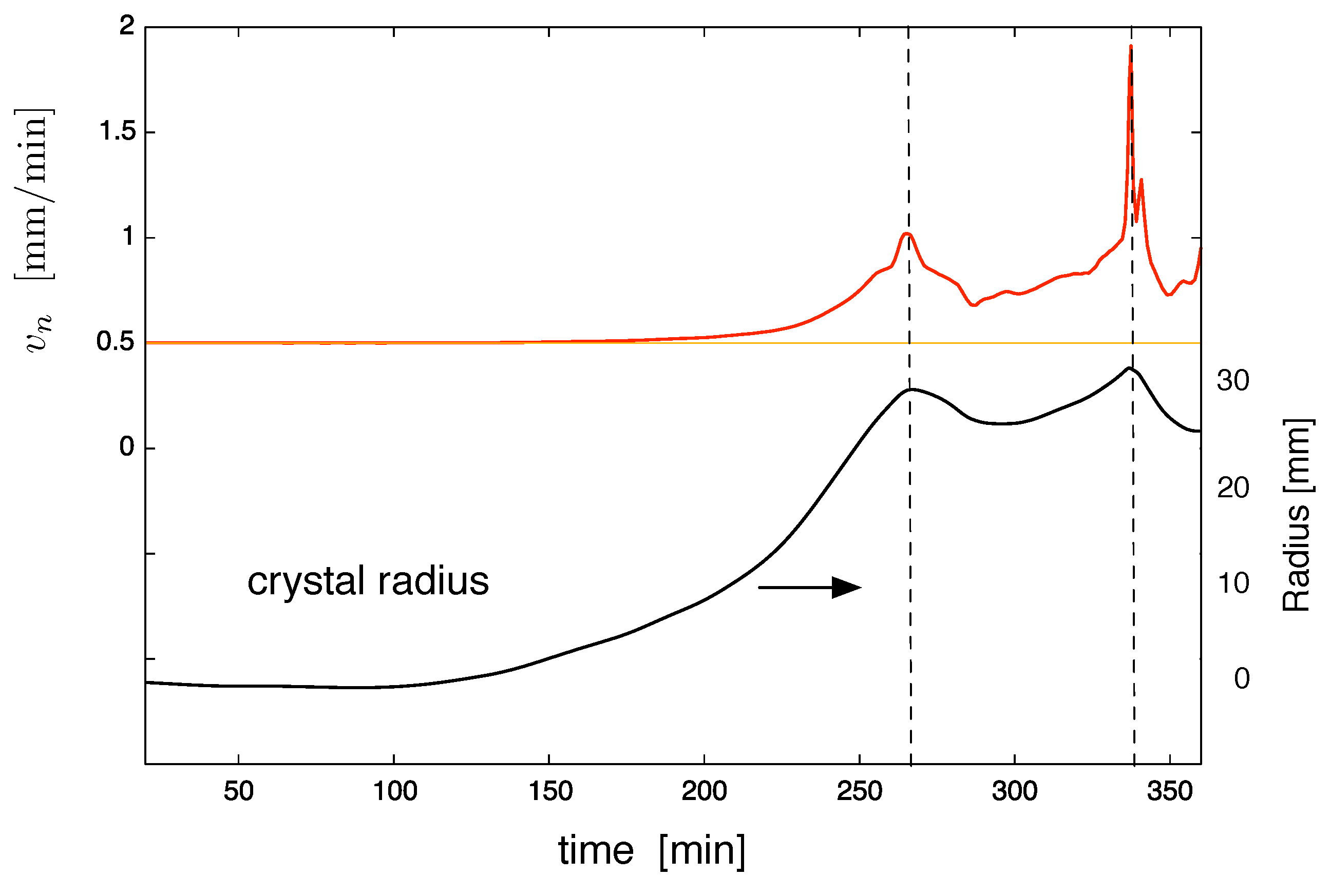
. The growth velocity was computed before the thermal calculation with Elmer starts and was not adapted later. This meant that the latent heat production corresponded to the evolution of a flat interface. Latent heat effects due to changes in the interface shape were not considered. The second instability occurred near the end of the process. For a better comparison, the crystal radius is also plotted in
Figure 5. Please note that the plot was versus process time and not versus crystal length. Therefore, the shape given by the plot of the crystal radius differed from that of the crystal shape. We also show the result if only the change in the melt level was taken into account for computing
and the change of the meniscus height was neglected (light orange curve). In the regions where the crystal radius was going from an increasing to a decreasing one, a strong peak in power occurred. In these regions, the large change of
led to a significant change of
(see Equation (
1)) and the melt volume beneath the crystal. Therefore, taking into account the effect of this melt volume in the computation of the growth velocity had a strong impact on the power consumption.
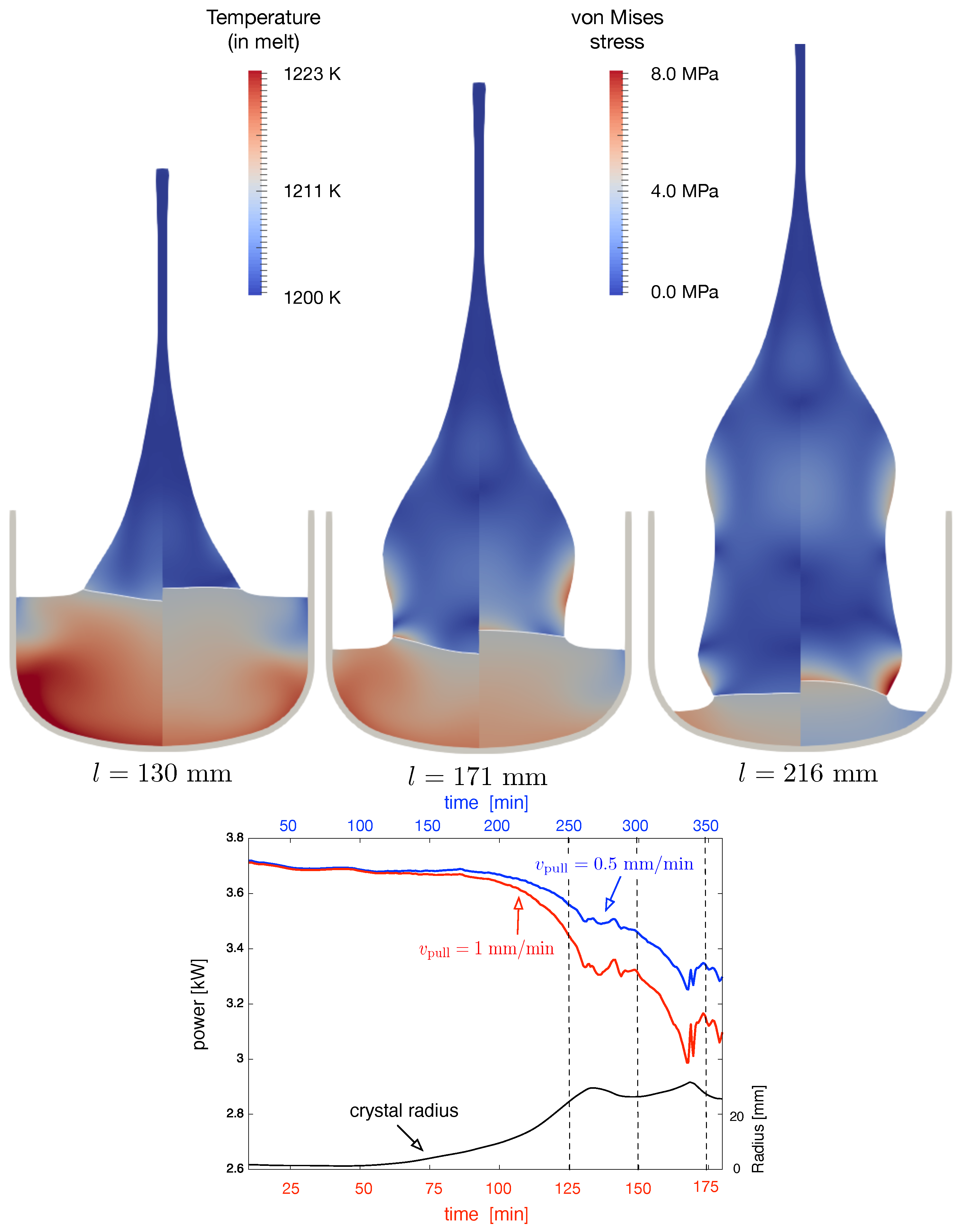
One of the key process parameters was the pulling velocity. The higher the velocity, the larger the amount of latent heat released and the lower the required power. For Case 2, we computed the process again for a pulling velocity of
. In
Figure 6, we show at the bottom the power consumption as a function of the process time. Please note that for the same length of the crystal, the process time was different for the two cases. The dotted lines indicate the growth stage where the von Mises stress in the crystal and the temperature in the melt are shown on the left hand side. For each stage, the left part and right part show the results for
and
, respectively. The reduced power consumption for
had a strong impact on the temperature in the melt (see
Figure 6 top). The melt would freeze at the top in the vicinity of the crucible. This meant that the position of the crucible should be changed when applying a high pulling velocity. The von Mises stress depended significantly on the growth stage and was sometimes larger in one case and sometimes in the other. We would like to note that we took the shape of the crystal as observed in the experiment with
. Therefore, a general statement on stresses and possible dislocation multiplication cannot be made. However, the situation for the melt/crystal interface was clear: the interface for
was always concave, whereas for
, it was always convex. We would like to mention that with the algorithm developed, we could give any crystal shape as an input and check the optimal pulling velocity. As an illustration of how the growth velocity was changing during the growth process in Case 2, we show the
as a function of the process time in
Figure 7. One can see that the main deviations from the pulling velocity
were in the regions of increasing radius.
A transient or quasi-transient calculation was the prerequisite for computing the dislocation density. However, this was beyond the purpose of this paper, and we only wanted to make some simple calculations to estimate the situation for the two different growth cases. In the Alexander–Haasen model [
27], the multiplication of dislocations is given by (see the Nomenclature):
The effective strain is given by
with
and
.
D is the hardening factor. In this paper, we neglected the hardening effect and set
, the von Mises stress. For Ge,
, and the Peierls energy was
[
28]. The same value could be obtained from the data in Figure 10 of [
29] when choosing
for both temperatures. In addition, one obtains
. Taking
[
30], we obtain:
Typically, EPD is measured on three wafers: one in the cone, one at the beginning of the cylindrical part, and one at the end of the cylindrical part. On each wafer, measurements were made at the centre, at
and
, where
is the radius of the wafer. Measurements were done in two crystallographic directions
and
on a
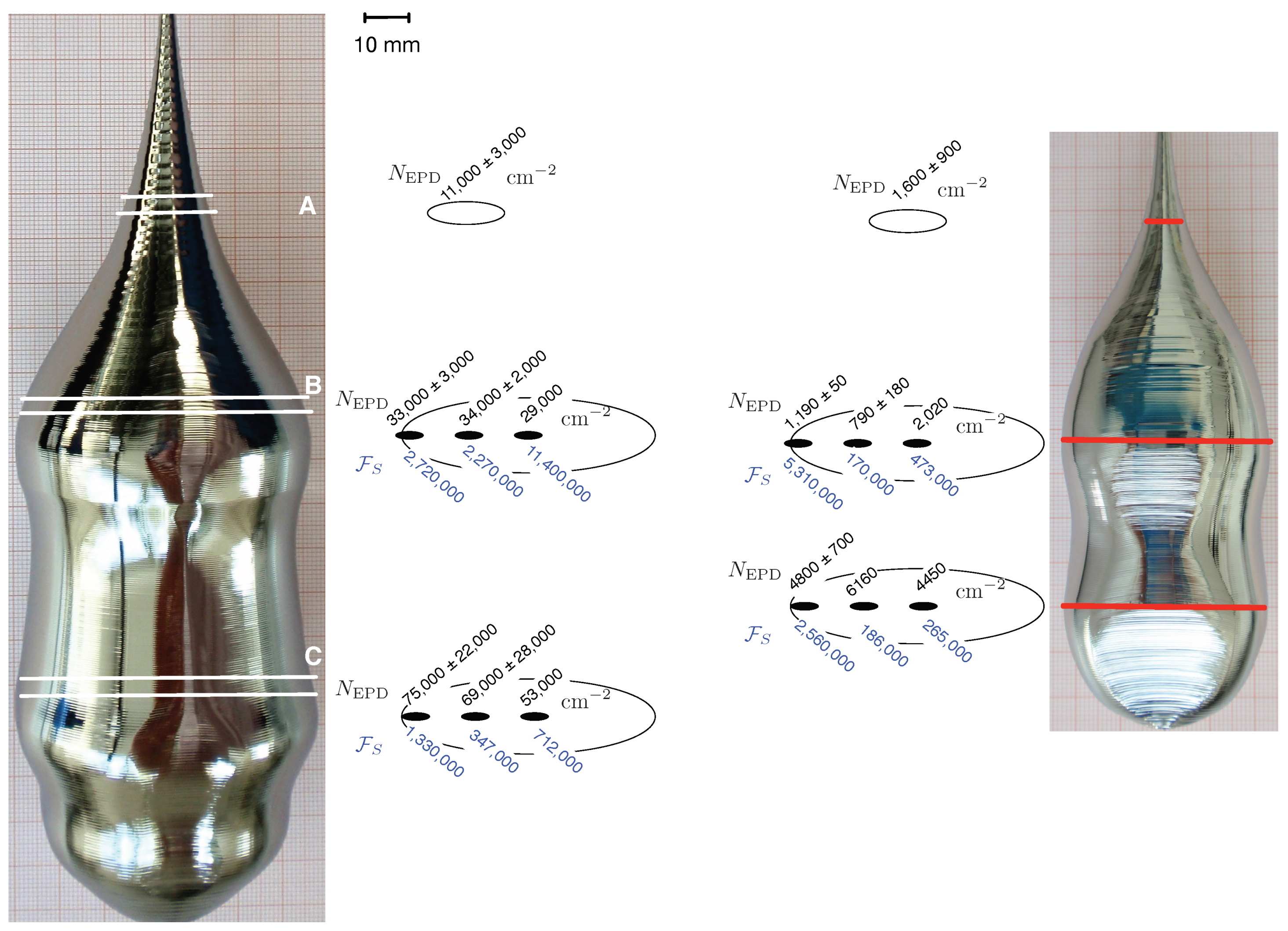
oriented plane. Because we performed axisymmetric calculations, we used the average value of the two directions. For the wafer in the cone, we only used one average value because the radius was much smaller than for the wafers from the cylindrical part. The EPD values
for Cases 1 and 2 are given in
Figure 8. For all data points with average values, we also show the maximum variation. EPD was much higher in Case 2 than in Case 1. Please note that in Case 1, argon was used instead of hydrogen, as in Case 2. We also would like to stress that the crystal in Case 2 was grown as a reference crystal, and the process was not optimized with respect to the dislocation densities. In order to make any comparison with our numerical calculations, we summed up the volume averaged multiplication factor
in a certain region in time:
These numbers are given in blue in
Figure 8. They were significant larger for Case 2 than for Case 1. Thus, the observed tendency in EPD was reflected in the numerical results. The EPD was between 10 and 30 times larger in Case 2 than in Case 1. The calculations exhibited a similar behavior, but the numbers at the centre in Case 2 and those at the rim for Case 1 showed a disagreement from the trend. Nevertheless, the calculation strategy could be already used to find the process conditions where the dislocation density was low. However, a further improvement of the model was required, where the plastic strain should be included in the stress computation (Equation (6)), which was demonstrated by Helbig et al. [
31]. In addition, the dislocation density should be computed using Equation (7).
