Atmospheric Air Plasma Treated SnS Films: An Efficient Electrocatalyst for HER

 , and
, and
Abstract
1. Introduction
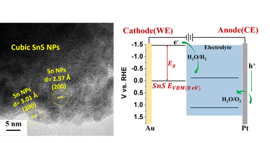
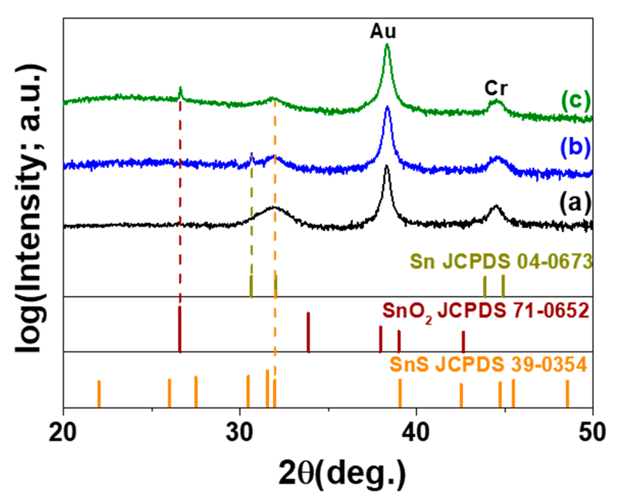
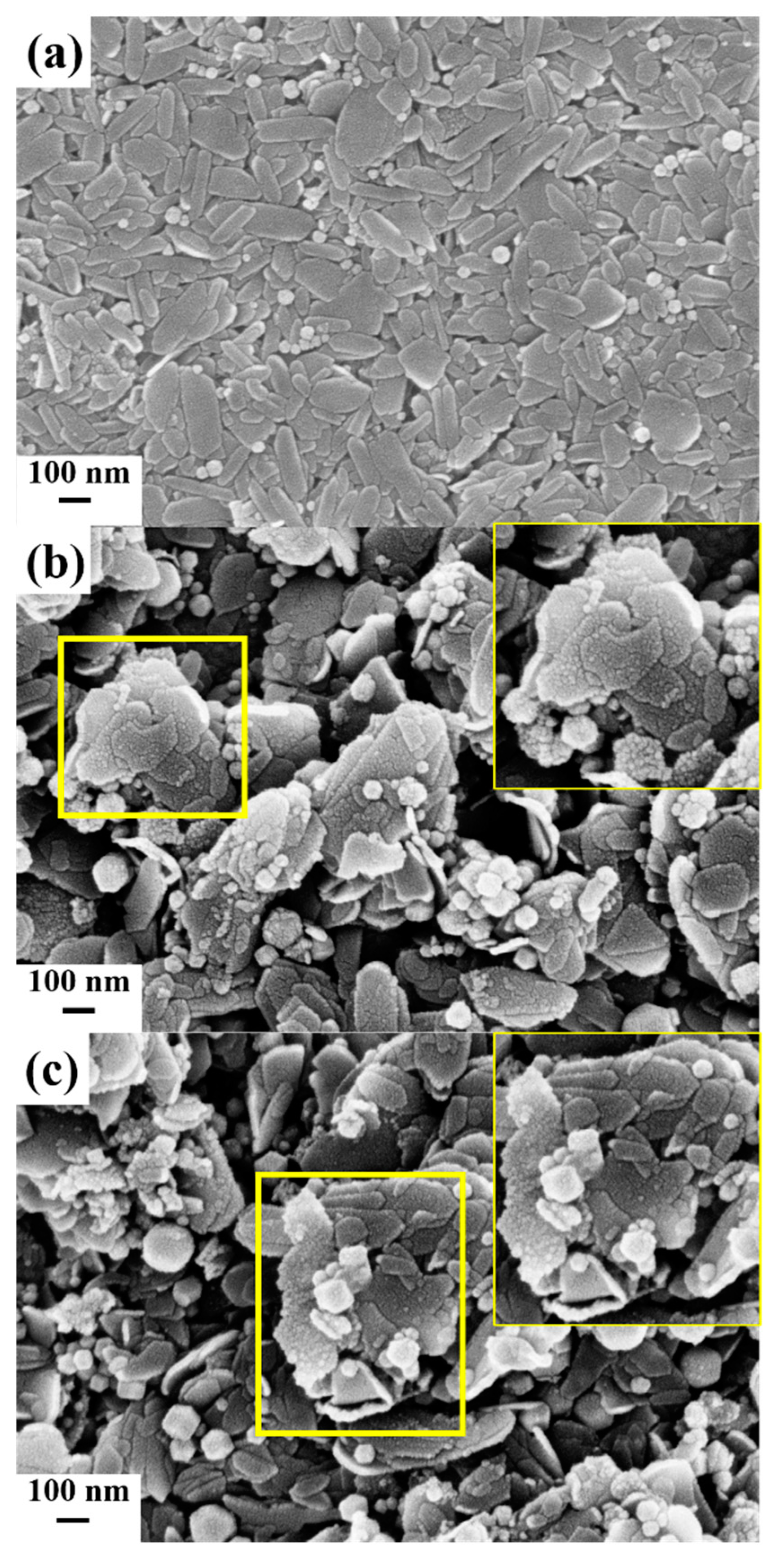
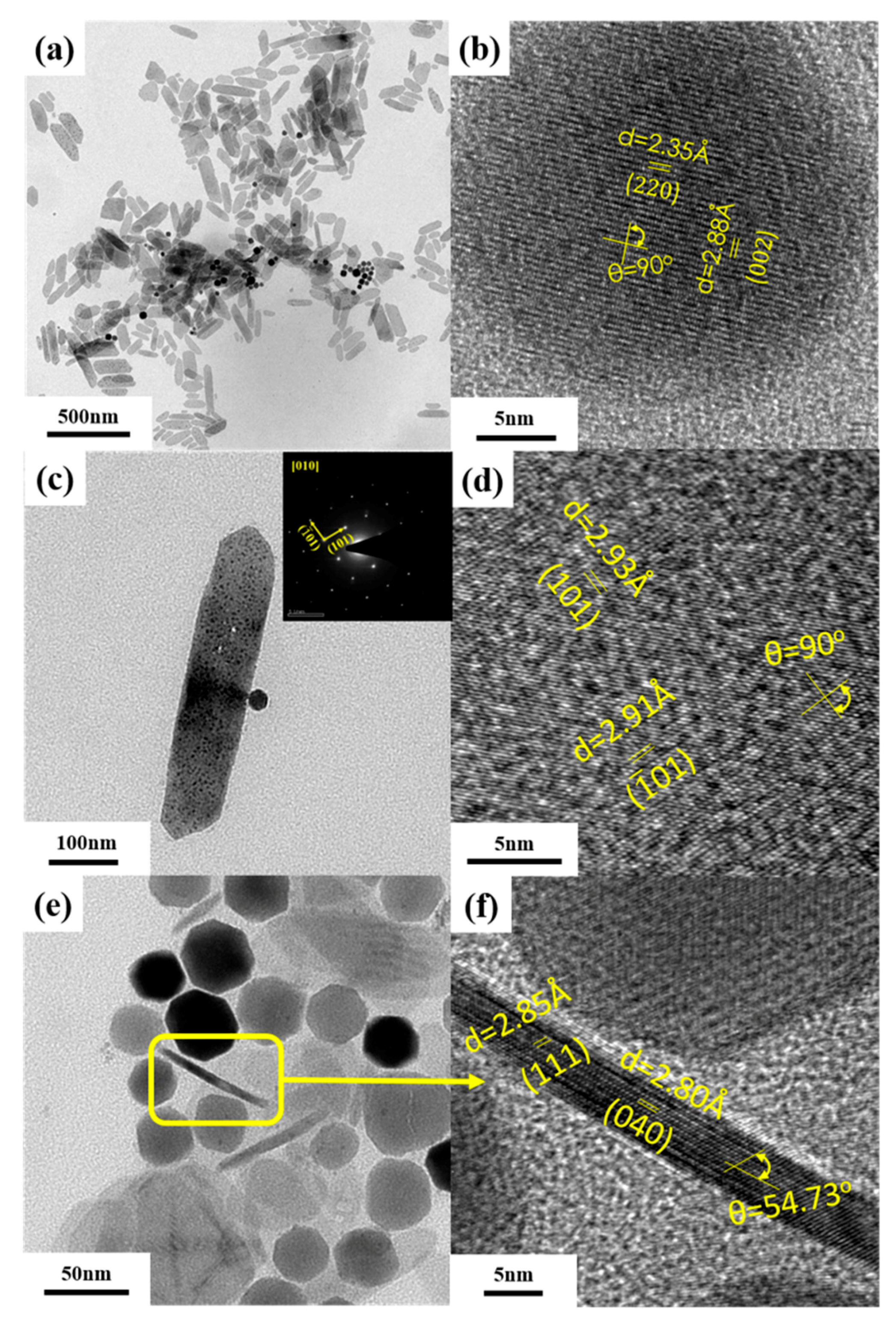
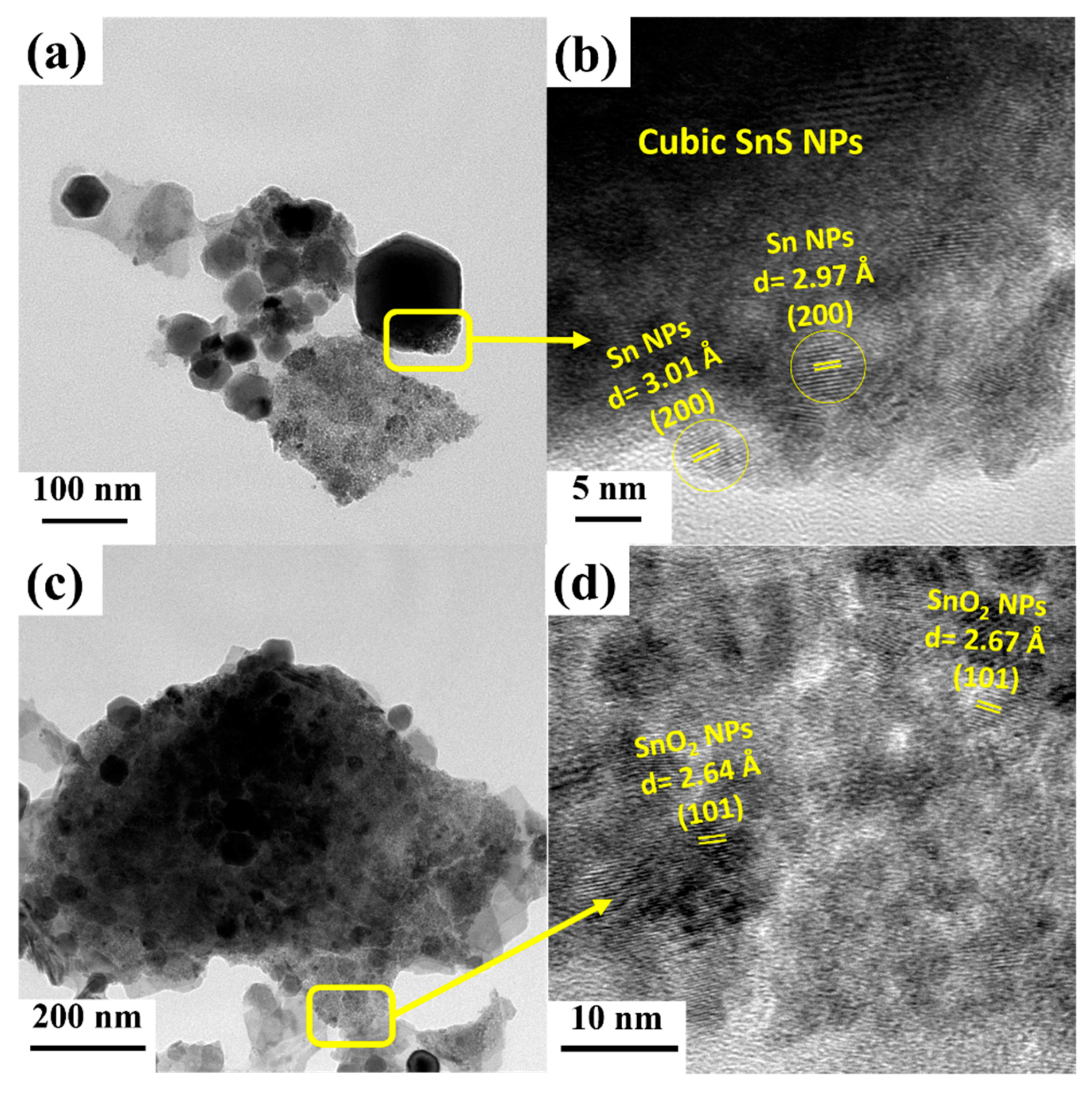
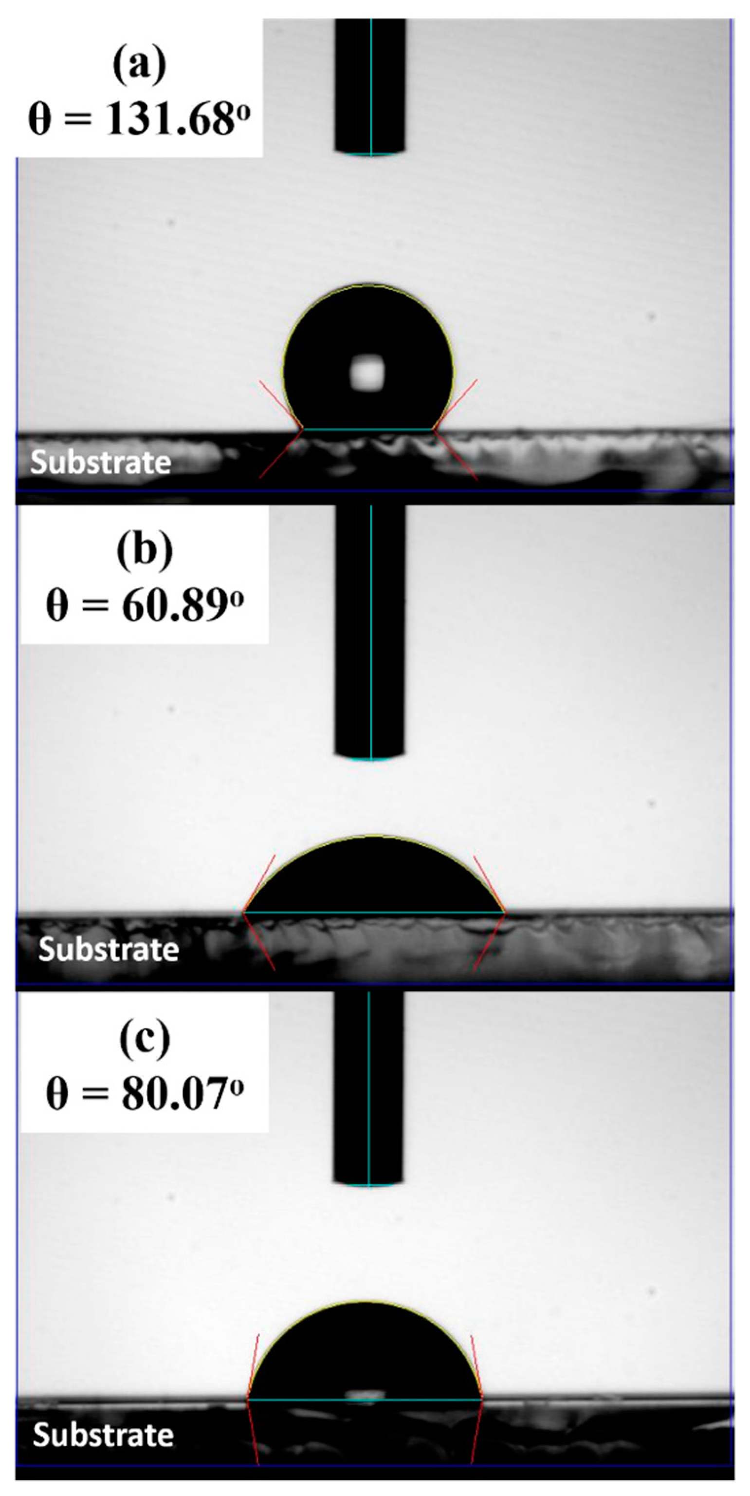
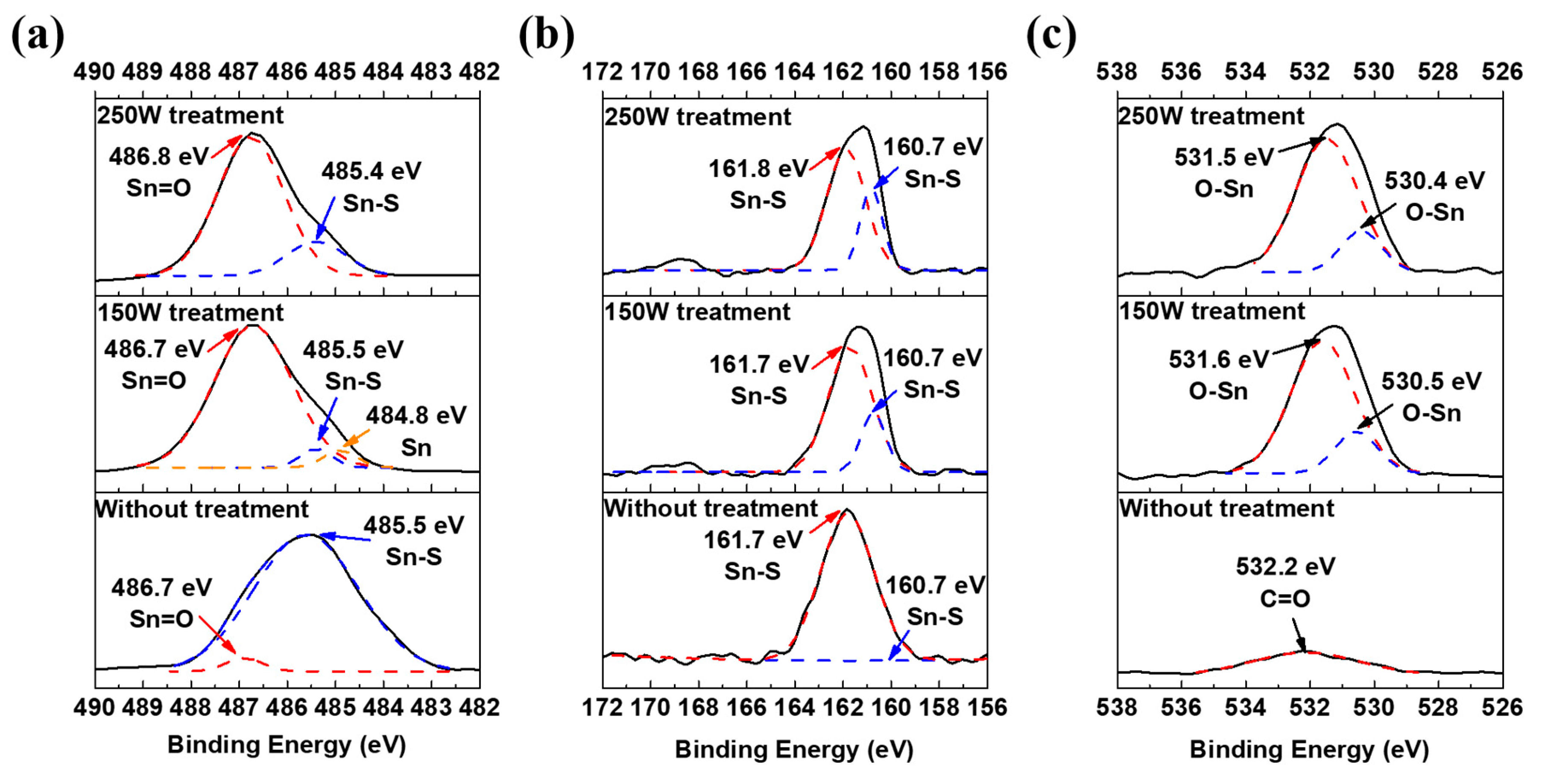
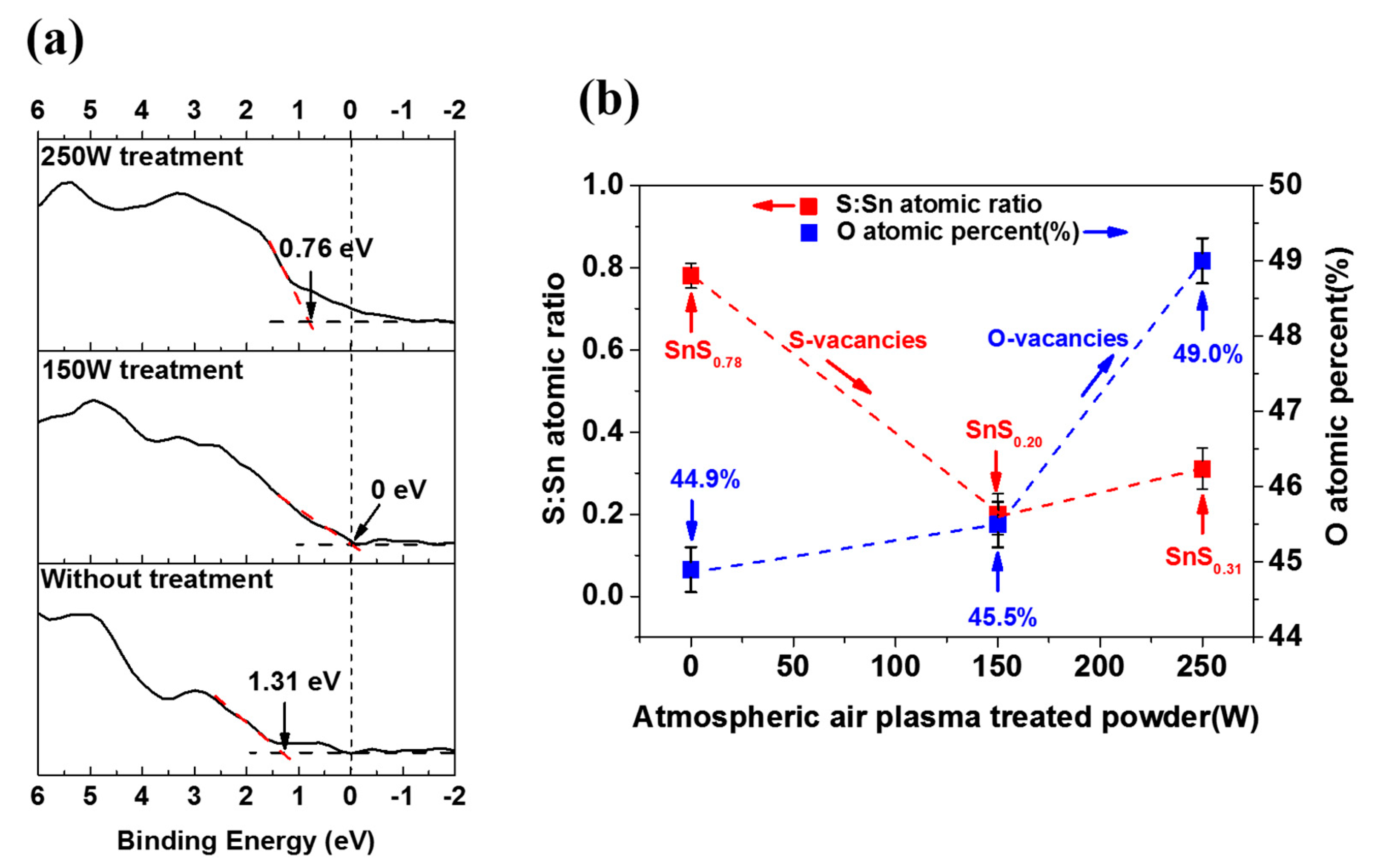
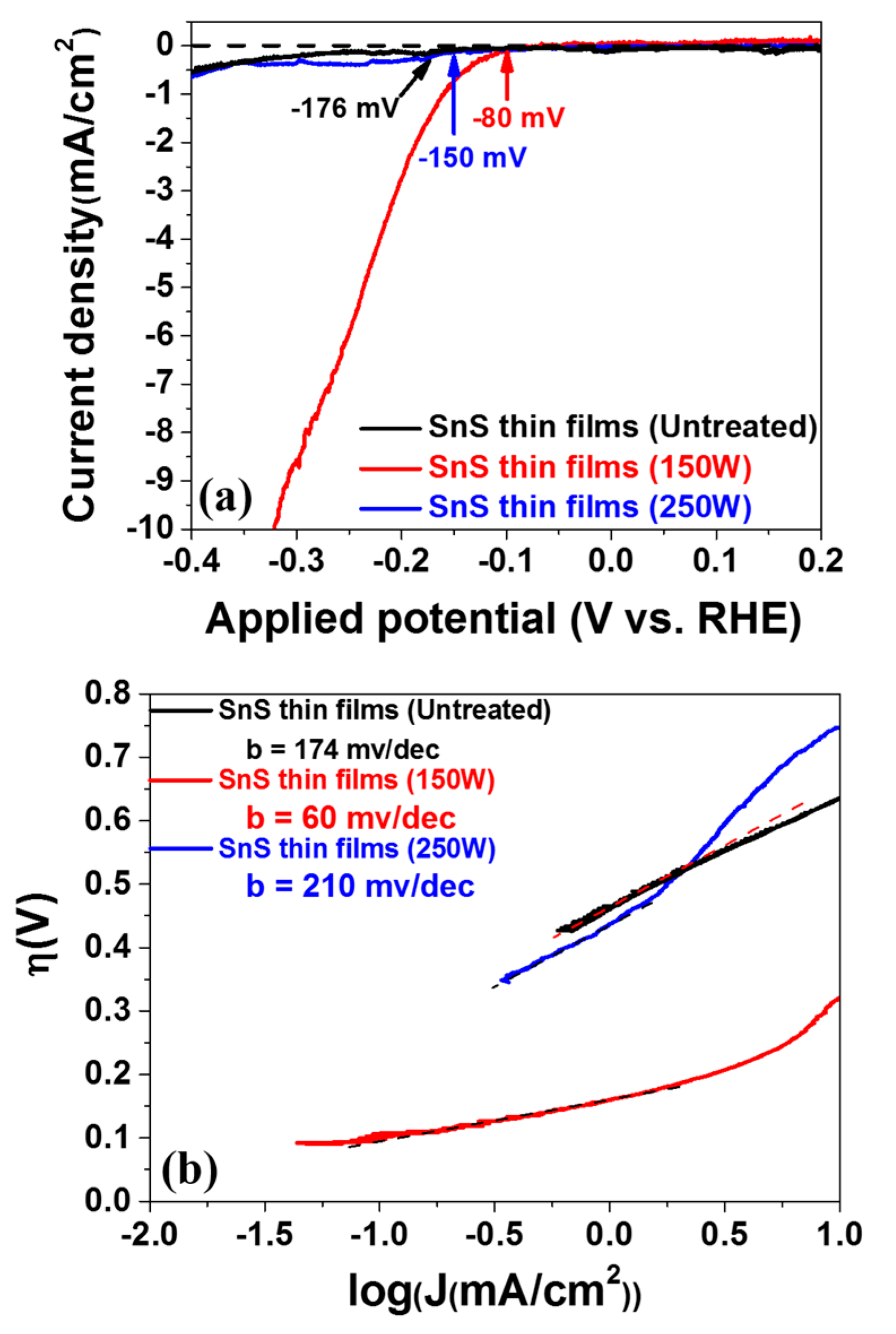
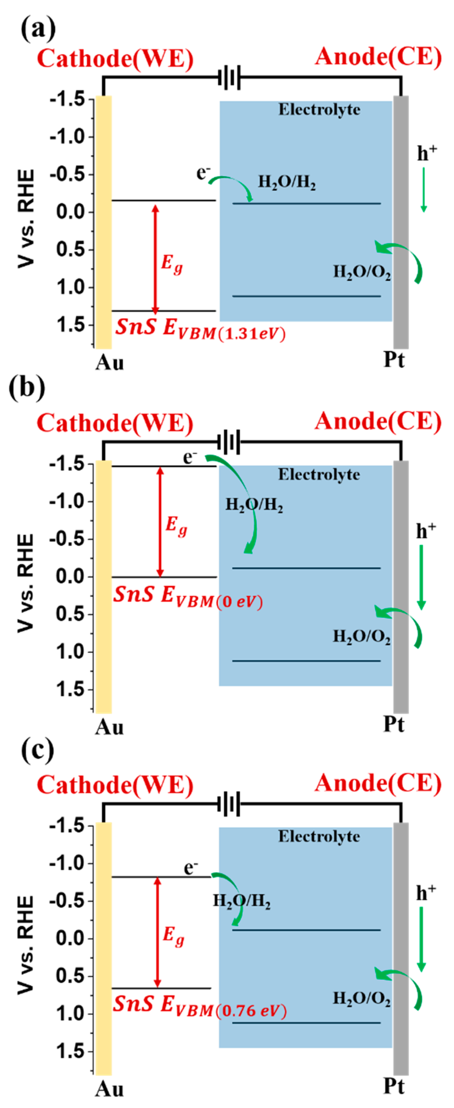
2. Results
3. Materials and Methods
3.1. Synthesis of Mixed Phase SnS Nanocrystals
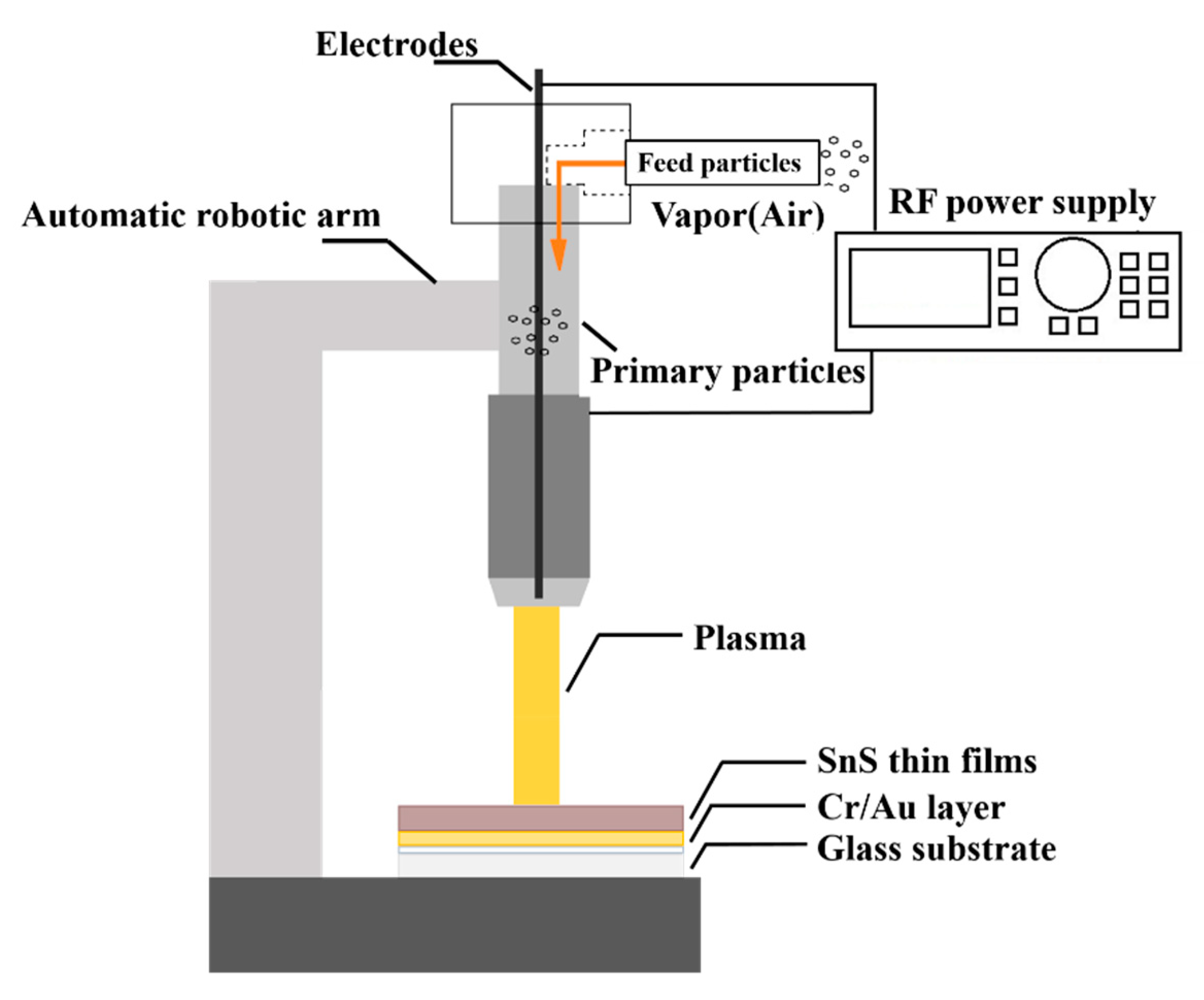
3.2. Atmospheric Air Plasma Treatment
3.3. Material Characterization
3.4. SnS Electrochemical Measurements
4. Conclusions
Supplementary Materials
Author Contributions
Funding
Acknowledgments
Conflicts of Interest
References
- Wang, F.M.; Shifa, T.A.; Zhan, X.Y.; Huang, Y.; Liu, K.L.; Cheng, Z.Z.; Jiang, C.; He, J. Recent advances in transition-metal dichalcogenide based nanomaterials for water splitting. Nanoscale 2015, 7, 19764–19788. [Google Scholar] [CrossRef] [PubMed]
- Gao, M.R.; Xu, Y.F.; Jiang, J.; Yu, S.H. Nanostructured metal chalcogenides: Synthesis, modification, and applications in energy conversion and storage devices. Chem. Soc. Rev. 2013, 42, 2986–3017. [Google Scholar] [CrossRef] [PubMed]
- Wu, C.L.; Huang, P.C.; Brahma, S.; Huang, J.L.; Wang, S.C. MoS2-MoO2 composite electrocatalysts by hot-injection method for hydrogen evolution reaction. Ceram. Int. 2017, 43, S621–S627. [Google Scholar] [CrossRef]
- Li, P.; Yang, Z.; Shen, J.; Nie, H.; Cai, Q.; Li, L.; Ge, M.; Gu, C.; Chen, X.A.; Yang, K. Subnanometer Molybdenum Sulfide on Carbon Nanotubes as a Highly Active and Stable Electrocatalyst for Hydrogen Evolution Reaction. ACS Appl. Mater. Interfaces 2016, 8, 3543–3550. [Google Scholar] [CrossRef] [PubMed]
- Sang, Y.H.; Zhao, Z.H.; Zhao, M.W.; Hao, P.; Leng, Y.H.; Liu, H. From UV to Near-Infrared, WS2 Nanosheet: A Novel Photocatalyst for Full Solar Light Spectrum Photodegradation. Adv. Mater. 2015, 27, 363–369. [Google Scholar] [CrossRef] [PubMed]
- Xie, J.F.; Wang, R.X.; Bao, J.; Zhang, X.D.; Zhang, H.; Li, S.; Xie, Y. Zirconium trisulfide ultrathin nanosheets as efficient catalysts for water oxidation in both alkaline and neutral solutions. Inorg. Chem. Front. 2014, 1, 751–756. [Google Scholar] [CrossRef]
- Kafashan, H.; Azizieh, M.; Balak, Z. Electrochemical synthesis of nanostructured Se-doped SnS: Effect of Se-dopant on surface characterizations. Appl. Surf. Sci. 2017, 410, 186–195. [Google Scholar] [CrossRef]
- Kois, J.; Bereznev, S.; Maricheva, J.; Revathi, N. Electrochemical and photoelectrochemical characterization of SnS photoabsorber films. Mater. Sci. Semicond. Process. 2017, 58, 76–81. [Google Scholar] [CrossRef]
- Huang, P.C.; Shen, Y.M.; Brahma, S.; Shaikh, M.O.; Huang, J.L.; Wang, S.C. SnSx (x = 1, 2) Nanocrystals as Effective Catalysts for PhotoelectrochemicalWater Splitting. Catalysts 2017, 7, 252. [Google Scholar] [CrossRef]
- Huang, P.C.; Wang, H.I.; Brahma, S.; Wang, S.C.; Huang, J.L. Synthesis and characteristics of layered SnS2 nanostructures via hot injection method. J. Cryst. Growth 2017, 468, 162–168. [Google Scholar] [CrossRef]
- Patel, M.; Chavda, A.; Mukhopadhyay, I.; Kim, J.; Ray, A. Nanostructured SnS with inherent anisotropic optical properties for high photoactivity. Nanoscale 2016, 8, 2293–2303. [Google Scholar] [CrossRef] [PubMed]
- Shinde, S.S.; Sami, A.; Kim, D.H.; Lee, J.H. Nanostructured SnS-N-doped graphene as an advanced electrocatalyst for the hydrogen evolution reaction. Chem. Commun. 2015, 51, 15716–15719. [Google Scholar] [CrossRef] [PubMed]
- Zhao, B.; Wang, Z.X.; Chen, F.; Yang, Y.Q.; Gao, Y.; Chen, L.; Jiao, Z.; Cheng, L.L.; Jiang, Y. Three-Dimensional Interconnected Spherical Graphene Framework/SnS Nanocomposite for Anode Material with Superior Lithium Storage Performance: Complete Reversibility of Li2S. ACS Appl. Mater. Interfaces 2017, 9, 1407–1415. [Google Scholar] [CrossRef] [PubMed]
- Hortikar, S.S.; Kadam, V.S.; Rathi, A.B.; Jagtap, C.V.; Pathan, H.M.; Mulla, I.S.; Adhyapak, P.V. Synthesis and deposition of nanostructured SnS for semiconductor-sensitized solar cell. J. Solid State Electrochem. 2017, 21, 2707–2712. [Google Scholar] [CrossRef]
- Chia, X.Y.; Lazar, P.; Sofer, Z.; Luxa, J.; Pumera, M. Layered SnS versus SnS2: Valence and Structural implications on Electrochemistry and Clean Energy Electrocatalysis. J. Phys. Chem. C 2016, 120, 24098–24111. [Google Scholar] [CrossRef]
- Ennaoui, A.; Fiechter, S.; Jaegermann, W.; Tributsch, H. Photoelectrochemistry of Highly Quantum Efficient Single-Crystalline N-Fes2 (Pyrite). J. Electrochem. Soc. 1986, 133, 97–106. [Google Scholar] [CrossRef]
- Todorov, T.K.; Tang, J.; Bag, S.; Gunawan, O.; Gokmen, T.; Zhu, Y.; Mitzi, D.B. Beyond 11% Efficiency: Characteristics of State-of-the-Art Cu2ZnSn(S,Se)(4) Solar Cells. Adv. Energy Mater. 2013, 3, 34–38. [Google Scholar] [CrossRef]
- Wang, W.; Winkler, M.T.; Gunawan, O.; Gokmen, T.; Todorov, T.K.; Zhu, Y.; Mitzi, D.B. Device Characteristics of CZTSSe Thin-Film Solar Cells with 12.6% Efficiency. Adv. Energy Mater. 2014, 4, 1301465. [Google Scholar] [CrossRef]
- Chaki, S.H.; Chaudhary, M.D.; Deshpande, M.P. Effect of Indium and Antimony Doping on SnS Photoelectrochemical Solar Cells. Chin. Phys. Lett. 2014, 31, 10. [Google Scholar] [CrossRef]
- Sun, Y.F.; Gao, S.; Lei, F.C.; Xie, Y. Atomically-thin two-dimensional sheets for understanding active sites in catalysis. Chem. Soc. Rev. 2015, 44, 623–636. [Google Scholar] [CrossRef] [PubMed]
- Yin, Z.Y.; Chen, B.; Bosman, M.; Cao, X.H.; Chen, J.Z.; Zheng, B.; Zhang, H. Au Nanoparticle-Modified MoS2 Nanosheet-Based Photoelectrochemical Cells for Water Splitting. Small 2014, 10, 3537–3543. [Google Scholar] [CrossRef] [PubMed]
- Gomez, A.; Martinez, H.; Calixto-Rodriguez, M.; Avellaneda, D.; Reyes, P.G.; Flores, O. Modification of optical and electrical properties of chemical bath deposited SnS using O-2 plasma treatments. Appl. Surf. Sci. 2013, 275, 273–277. [Google Scholar] [CrossRef]
- Chu, X.M.S.; Li, D.O.; Green, A.A.; Wang, Q.H. Formation of MoO3 and WO3 nanoscrolls from MoS2 and WS2 with atmospheric air plasma. J. Mater. Chem. C 2017, 5, 11301–11309. [Google Scholar] [CrossRef]
- Lisco, F.; Shaw, A.; Wright, A.; Walls, J.M.; Iza, F. Atmospheric-pressure plasma surface activation for solution processed photovoltaic devices. Sol. Energy 2017, 146, 287–297. [Google Scholar] [CrossRef]
- Lin, T.; Kang, B.; Jeon, M.; Huffman, C.; Jeon, J.; Lee, S.; Han, W.; Lee, J.; Lee, S.; Yeom, G.; et al. Controlled Layer-by-Layer Etching of MoS2. ACS Appl. Mater. Interfaces 2015, 7, 15892–15897. [Google Scholar] [CrossRef] [PubMed]
- Shin, Y.J.; Wang, Y.Y.; Huang, H.; Kalon, G.; Wee, A.T.S.; Shen, Z.X.; Bhatia, C.S.; Yang, H. Surface-Energy Engineering of Graphene. Langmuir 2010, 26, 3798–3802. [Google Scholar] [CrossRef] [PubMed]
- Zhu, H.; Qin, X.Y.; Cheng, L.X.; Azcatl, A.; Kim, J.; Wallace, R.M. Remote Plasma Oxidation and Atomic Layer Etching of MoS2. ACS Appl. Mater. Interfaces 2016, 8, 19119–19126. [Google Scholar] [CrossRef] [PubMed]
- Dou, S.; Tao, L.; Huo, J.; Wang, S.Y.; Dai, L.M. Etched and doped Co9S8/graphene hybrid for oxygen electrocatalysis. Energy Environ. Sci. 2016, 9, 1320–1326. [Google Scholar] [CrossRef]
- Li, H.; Tsai, C.; Koh, A.L.; Cai, L.L.; Contryman, A.W.; Fragapane, A.H.; Zhao, J.H.; Han, H.S.; Manoharan, H.C.; Abild-Pedersen, F.; et al. Activating and optimizing MoS2 basal planes for hydrogen evolution through the formation of strained sulphur vacancies. Nat. Mater. 2016, 15, 48. [Google Scholar] [CrossRef] [PubMed]
- Huang, Y.; Wu, J.; Xu, X.F.; Ho, Y.D.; Ni, G.X.; Zou, Q.; Koon, G.K.W.; Zhao, W.J.; Castro Neto, A.H.; Eda, G.; et al. An innovative way of etching MoS2: Characterization and mechanistic investigation. Nano Res. 2013, 6, 200–207. [Google Scholar] [CrossRef]
- Zhang, N.; Zhao, Q.; Han, X.P.; Yang, J.G.; Chen, J. Pitaya-like Sn@C nanocomposites as high-rate and long-life anode for lithium-ion batteries. Nanoscale 2014, 6, 2827–2832. [Google Scholar] [CrossRef] [PubMed]
- Wang, X.L.; Wang, X.; Di, Q.Y.; Zhao, H.L.; Liang, B.; Yang, J.K. Mutual Effects of Fluorine Dopant and Oxygen Vacancies on Structural and Luminescence Characteristics of F Doped SnO2 Nanoparticles. Materials 2017, 10, 1398. [Google Scholar] [CrossRef] [PubMed]
- Huang, P.C.; Huang, J.L.; Wang, S.C.; Shaikh, M.O.; Lin, C.Y. Photoelectrochemical properties of orthorhombic and metastable phase SnS nanocrystals synthesized by a facile colloidal method. Thin Solid Films 2015, 596, 135–139. [Google Scholar] [CrossRef]
- Herron, S.M.; Tanskanen, J.T.; Roelofs, K.E.; Bent, S.F. Highly Textured Tin(II) Sulfide Thin Films Formed from Sheetlike Nanocrystal Inks. Chem. Mater. 2014, 26, 7106–7113. [Google Scholar] [CrossRef]
- Reddy, N.K. Growth-Temperature Dependent Physical Properties of SnS Nanocrystalline Thin Films. ECS J. Solid State Sci. Technol. 2013, 2, 259–263. [Google Scholar] [CrossRef]
- Whittles, T.J.; Burton, L.A.; Skelton, J.M.; Walsh, A.; Veal, T.D.; Dhanak, V.R. Band Alignments, Valence Bands, and Core Levels in the Tin Sulfides SnS, SnS2, and Sn2S3: Experiment and Theory. Chem. Mater. 2016, 28, 3718–3726. [Google Scholar] [CrossRef]
- Zeng, Y.; Luo, J.Z.; Wang, Y.Z.; Qiao, L.; Zou, B.; Zheng, W.T. Controllable formation of multi-layered SnO2@Fe2O3 sandwich cubes as a high-performance anode for Li-ion batteries. Nanoscale 2017, 9, 17576–17584. [Google Scholar] [CrossRef] [PubMed]
- Burton, L.A.; Whittles, T.J.; Hesp, D.; Linhart, W.M.; Skelton, J.M.; Hou, B.; Webster, R.F.; O’Dowd, G.; Reece, C.; Cherns, D.; et al. Electronic and optical properties of single crystal SnS2: An earth-abundant disulfide photocatalyst. J. Mater. Chem. A 2016, 4, 1312–1318. [Google Scholar] [CrossRef]
- Liang, B.Y.J.; Shen, Y.M.; Wang, S.C.; Huang, J.L. The influence of reaction temperatures and volume of oleic acid to synthesis SnS nanocrystals by using thermal decomposition method. Thin Solid Films 2013, 549, 159–164. [Google Scholar] [CrossRef]
- Conway, B.E.; Tilak, B.V. Interfacial processes involving electrocatalytic evolution and oxidation of H-2, and the role of chemisorbed H. Electrochim. Acta 2002, 47, 3571–3594. [Google Scholar] [CrossRef]
- Chen, W.F.; Wang, C.H.; Sasaki, K.; Marinkovic, N.; Xu, W.; Muckerman, J.T.; Zhu, Y.; Adzic, R.R. Highly active and durable nanostructured molybdenum carbide electrocatalysts for hydrogen production. Energy Environ. Sci. 2013, 6, 943–951. [Google Scholar] [CrossRef]
- Ma, L.; Zhou, X.P.; Xu, X.Y.; Xu, L.M.; Zhang, L.L.; Chen, W.X. One-step hydrothermal synthesis of few-layered and edge-abundant MoS2/C nanocomposites with enhanced electrocatalytic performance for hydrogen evolution reaction. Adv. Powder Technol. 2015, 26, 1273–1280. [Google Scholar] [CrossRef]
- Nikam, R.D.; Lu, A.Y.; Sonawane, P.A.; Kumar, U.R.; Yadav, K.; Li, L.J.; Chen, Y.T. Three-Dimensional Heterostructures of MoS2 Nanosheets on Conducting MoO2 as an Efficient Electrocatalyst To Enhance Hydrogen Evolution Reaction. ACS Appl. Mater. Interfaces 2015, 7, 23328–23335. [Google Scholar] [CrossRef] [PubMed]
- Shifa, T.A.; Wang, F.M.; Cheng, Z.Z.; Zhan, X.Y.; Wang, Z.X.; Liu, K.L.; Safdar, M.; Sun, L.F.; He, J. A vertical-oriented WS2 nanosheet sensitized by graphene: An advanced electrocatalyst for hydrogen evolution reaction. Nanoscale 2015, 7, 14760–14765. [Google Scholar] [CrossRef] [PubMed]
- Yu, S.; Kim, J.; Yoon, K.R.; Jung, J.W.; Oh, J.; Kim, I.D. Rational Design of Efficient Electrocatalysts for Hydrogen Evolution Reaction: Single Layers of WS2 Nanoplates Anchored to Hollow Nitrogen-Doped Carbon Nanofibers. ACS Appl. Mater. Interfaces 2015, 7, 28116–28121. [Google Scholar] [CrossRef] [PubMed]
- Zou, M.L.; Chen, J.D.; Xiao, L.F.; Zhu, H.; Yang, T.T.; Zhang, M.; Du, M.L. WSe2 and W(SexS1−x)2 nanoflakes grown on carbon nanofibers for the electrocatalytic hydrogen evolution reaction. J. Mater. Chem. A 2015, 3, 18090–18097. [Google Scholar] [CrossRef]
- Chang, Y.H.; Wu, F.Y.; Chen, T.Y.; Hsu, C.L.; Chen, C.H.; Wiryo, F.; Wei, K.H.; Chiang, C.Y.; Li, L.J. Three- Dimensional Molybdenum Sulfi de Sponges for Electrocatalytic Water Splitting. Small 2014, 10, 895–900. [Google Scholar] [CrossRef] [PubMed]
- Chang, Y.H.; Nikam, R.D.; Lin, C.T.; Huang, J.K.; Tseng, C.C.; Hsu, C.L.; Cheng, C.C.; Su, C.Y.; Li, L.J.; Chua, D.H.C. Enhanced Electrocatalytic Activity of MoSx on TCNQ-Treated Electrode for Hydrogen Evolution Reaction. ACS Appl. Mater. Interfaces 2014, 6, 17679–17685. [Google Scholar] [CrossRef] [PubMed]
- Huang, P.-C.; Shaikh, M.O.; Wang, S.-C. Structural and optoelectronic properties of alloyed SnxMn1−xS thin films. Adv. Powder Technol. 2016, 27, 964–970. [Google Scholar] [CrossRef]


| Sample Name | VBM | Atom % (Sn) | Atom % (S) | Atom % (O) | S/Sn Ratio |
|---|---|---|---|---|---|
| Without AAPT | 1.31 | 30.8 | 24.3 | 44.9 | 0.78 |
| 150 W AAPT | 0 | 45.4 | 9.1 | 45.5 | 0.20 |
| 250 W AAPT | 0.76 | 38.9 | 12.1 | 49.0 | 0.31 |
| Sample Name | Onset (mV) | Current Density (−325 mV) | Tafel Slope |
|---|---|---|---|
| Without AAPT | −176 mV | −0.224 mA/cm2 | 174 mV/dec |
| 150 W AAPT | −80 mV | −10 mA/cm2 | 60 mV/dec |
| 250 W AAPT | −150 mV | −0.394 mA/cm2 | 210 mV/dec |
© 2018 by the authors. Licensee MDPI, Basel, Switzerland. This article is an open access article distributed under the terms and conditions of the Creative Commons Attribution (CC BY) license (http://creativecommons.org/licenses/by/4.0/).
Share and Cite
Huang, P.-C.; Brahma, S.; Liu, P.-Y.; Huang, J.-L.; Wang, S.-C.; Weng, S.-C.; Shaikh, M.O. Atmospheric Air Plasma Treated SnS Films: An Efficient Electrocatalyst for HER. Catalysts 2018, 8, 462. https://doi.org/10.3390/catal8100462
Huang P-C, Brahma S, Liu P-Y, Huang J-L, Wang S-C, Weng S-C, Shaikh MO. Atmospheric Air Plasma Treated SnS Films: An Efficient Electrocatalyst for HER. Catalysts. 2018; 8(10):462. https://doi.org/10.3390/catal8100462
Chicago/Turabian StyleHuang, Po-Chia, Sanjaya Brahma, Po-Yen Liu, Jow-Lay Huang, Sheng-Chang Wang, Shao-Chieh Weng, and Muhammad Omar Shaikh. 2018. "Atmospheric Air Plasma Treated SnS Films: An Efficient Electrocatalyst for HER" Catalysts 8, no. 10: 462. https://doi.org/10.3390/catal8100462
APA StyleHuang, P.-C., Brahma, S., Liu, P.-Y., Huang, J.-L., Wang, S.-C., Weng, S.-C., & Shaikh, M. O. (2018). Atmospheric Air Plasma Treated SnS Films: An Efficient Electrocatalyst for HER. Catalysts, 8(10), 462. https://doi.org/10.3390/catal8100462