Article

Effect of the Deposition of Vanadium-Oxide on the Photocatalytic Activity of TiO2 Nanotubes and Its Photodiode Performance Interfaced with CH3NH3PbI3 Single Crystal

by
Jelena Vujančević
1,*,†,
Pavao Andričević
2,3,
Veljko Djokić
2,4,
Vladimir Blagojević
5,
Vera P. Pavlović
6,
Jovana Ćirković
7,
Endre Horváth
2,8,
László Forró
2,9,
Abdennaceur Karoui
10,
Vladimir B. Pavlović
11 and
Djordje Janaćković
4
1
Institute of Technical Sciences of SASA, Knez Mihailova 35/IV, 11000 Belgrade, Serbia
2
Ecole Polytechnique Fédérale de Lausanne, Laboratory of Physics of Complex Matter, CH-1015 Lausanne, Switzerland
3
Department of Physics, Technical University of Denmark, DTU Risø Campus, 4000 Lyngby, Denmark
4
Faculty of Technology and Metallurgy, University of Belgrade, Karnegijeva 4, 11120 Belgrade, Serbia
5
TBP Software, Solunska 11, 11000 Belgrade, Serbia
6
Faculty of Mechanical Engineering, University of Belgrade, Kraljice Marije 16, 11120 Belgrade, Serbia
7
University of Belgrade, Institute for Multidisciplinary Research, Kneza Višeslava 1, 11000 Belgrade, Serbia
8
Haute école du Paysage, D’ingénierie et D’architecture de Genève—HEPIA, 1202 Genève, Switzerland
9
University of Notre Dame, 204A Nieuwland Science Hall, Notre Dame, IN 46556, USA
10
Department of Physics, North Carolina Central University, 1801 Fayetteville St., Durham, NC 27707, USA
11
Faculty of Agriculture, University of Belgrade, Nemanjina 6, 11080 Belgrade-Zemun, Serbia
*
Author to whom correspondence should be addressed.
Current address: Department for Nanostructured Materials, Institute Jožef Stefan, Jamova cesta 39, 1000 Ljubljana, Slovenia.
Catalysts 2023, 13(2), 352; https://doi.org/10.3390/catal13020352
Submission received: 29 December 2022 / Revised: 24 January 2023 / Accepted: 31 January 2023 / Published: 4 February 2023
(This article belongs to the Special Issue Advanced Materials for Application in Catalysis)

Abstract

:
In this study, we report the influence of vanadium oxide (VO), as a photosensitive component, on the photoactivity of TiO2 nanotubes (TNTs). A series of TNTs of varying tube diameter were synthesized by the anodization of titanium foils at different voltages, while vanadium oxide was deposited on TNTs by wet chemical deposition. An improvement in the optical properties of nanotubes was observed after the deposition of vanadium oxide. An improvement in the optical properties (redshift in UV-Vis spectra) of TNTs and TNT/VO was noted. The photocatalytic activity was improved with increasing tube diameter, while it was weakened after the deposition of VO. Furthermore, photoactivity was investigated in photodiodes based on TNTs or TNT/VO and single crystals of CH3NH3PbI3. The photoelectric measurement revealed that different TNT diameters did not influence the I-V characteristic of the photodiodes, while the deposition of VO improved the photocurrent for smaller TNTs.

1. Introduction

Due to its great optical and electrical properties, TiO2 is used for various light-induced applications such as solar cells [1], optoelectronics [2], photocatalysis [3], self-cleaning materials [4] or water-splitting for hydrogen production [5]. To improve its photoactivity, it is necessary to speed up the transport of electrons and holes and to enable the better separation of electrons and holes to reduce their recombination rate.
For better and faster charge carrier transport, a unidirectional path is desired, which can be obtained by synthesizing 1 D morphology [6]. According to Liu et al. [7] the height, wall thickness, and diameter of nanotubes have a significant effect on the photocatalytic activity of TiO2. Nanotubular morphology can be obtained by the anodization of titanium foil optimized via operative conditions: applied voltage, anodization time, and type of electrolyte [8]. Therefore, the duration of anodization influences the height of nanotubes, while applied voltage influences the nanotube diameter [9].
Furthermore, charge carrier separation can be improved by coupling TiO2 with other sensitizers such as quantum dots [10], transition metals [11], organometallic salt [12], etc. A heterojunction can be formed between TiO2 and metal oxides with narrower bandgaps, such as vanadium oxide. When TiO2 is coupled with V2O5, the Fermi levels of TiO2 and V2O5 equalize to achieve balance. However, the conduction band of V2O5 rises, becoming higher than the conduction band of TiO2, which represents a driving force for the transport of electrons from V2O5 to TiO2, and the transport of holes from TiO2 to V2O5. This cascade distribution of energy bands improves charge carrier separation, thus decreasing recombination and losses during photocatalysis [13].
The coupling of TiO2 with small bandgap semiconductors increases the charge separation of photogenerated electrons and holes. Liu et al. [14] observed suppressed electron–hole recombination and efficient separation of charge carriers on the TiO2@V2O5 core–shell interface. First, TiO2 hollow spheres were synthesized by a template method, which were further formed as core–shell hollow porous microspheres by a hydrothermal process assisted by a sol–gel method. Epifani et al. [15] modified the surface of TiO2 (anatase) nanoparticles with VOx via a sol–gel method. They proved that synergies between anatase and VOx increased the electric conductivity, voltage window, specific capacitance, and cycling stability. The 1D TiO2/V2O5 heterostructures were fabricated by electrospinning and sputtering [16]. Faster degradation of Rhodamine B dye was observed by TiO2/V2O5 nanofibers compared to pure TiO2 nanofibers. Klosek et al. [17] synthesized four different catalysts: TiO2/PVG (TiO2 monolayer supported on transparent porous borosilicate glass (PVG)), V/PVG (vanadium oxide monolayer supported on PVG), TiO2/V/PVG (one monolayer TiO2 supported on V/PVG), and V/TiO2/PVG (vanadium oxide supported on TiO2/PVG). Mixed catalysts (TiO2/V/PVG and V/TiO2/PVG) showed better photoactivity in comparison with V/PVG and TiO2/PVG due to the excitation of 3D electrons from V4+ into the TiO2 conduction band. They observed the importance of the ratio of V4+ and V5+, because V4+ may act as a recombination center under UV/visible radiation, while under visible radiation, V4+ is more active than V5+ centers.
Another way to improve photoactivity is to couple TiO2 with organic–inorganic perovskite such as methylammonium lead triiodide—MAPbI3 (CH3NH3PbI3). MAPbI3 has several advantages: it has a bandgap around 1.5–1.6 eV, a high absorption coefficient, and a long charge carrier diffusion length [18,19,20,21]. Elseman and coauthors [22] studied the influence of 0D and 1D morphology TiO2 on perovskite solar cells. They observed that the photocurrent density increased from 23.9 mA/cm2 for TiO2 nanoparticles to 25.5 mA/cm2 for TiO2 nanotube arrays, because nanotubes harvest more sunlight due to the Mie scattering effect. In our previous work [23], the influence of N doping on the photoactivity of TiO2 nanotubes/MAPbI3 interfaces was presented. It was observed that higher nitrogen concentration improved the photodiode photocurrent.
The aim of this work was to examine the influence of the TNT/VO interface on photocatalytic activity. Therefore, nanotubes with different diameters were synthesized, which were further coated by the deposition of vanadium oxide from solution at room temperature. Lastly, photoactivity of the TNT/VO and single-crystal CH3NH3PbI3 heterojunction was explored.

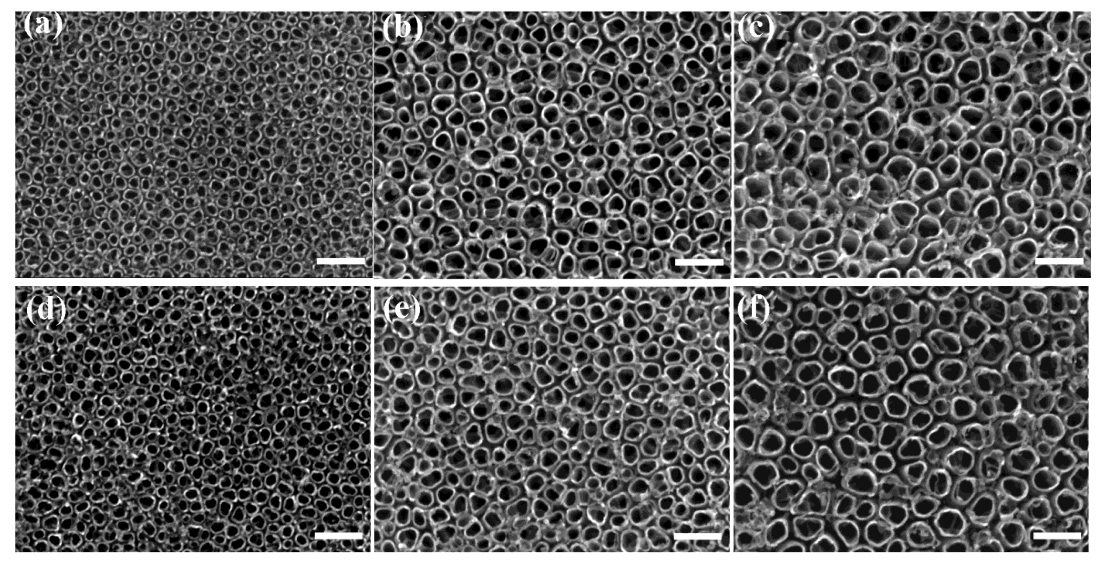
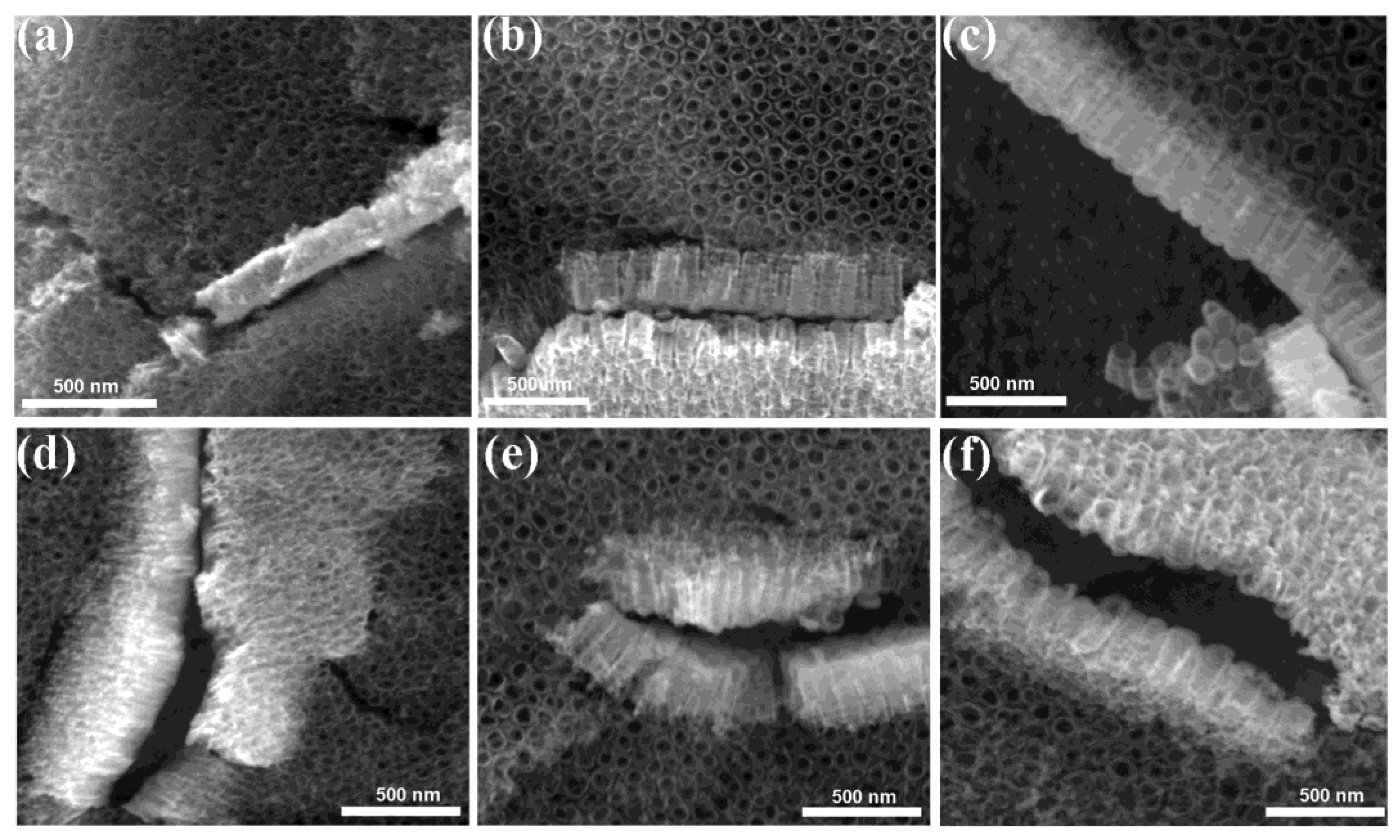
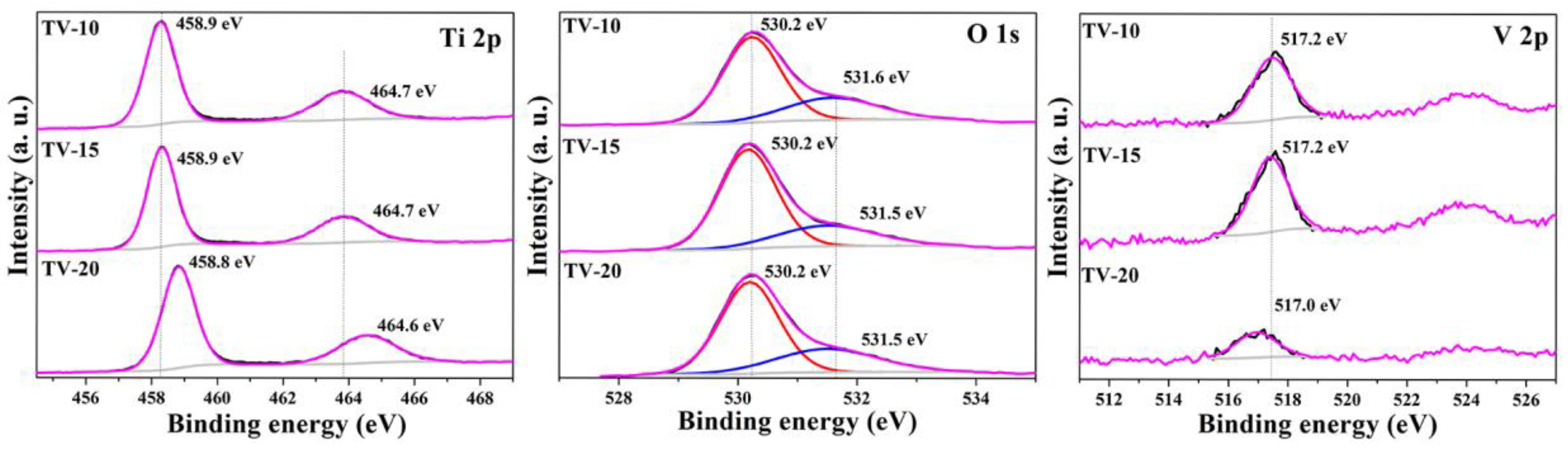
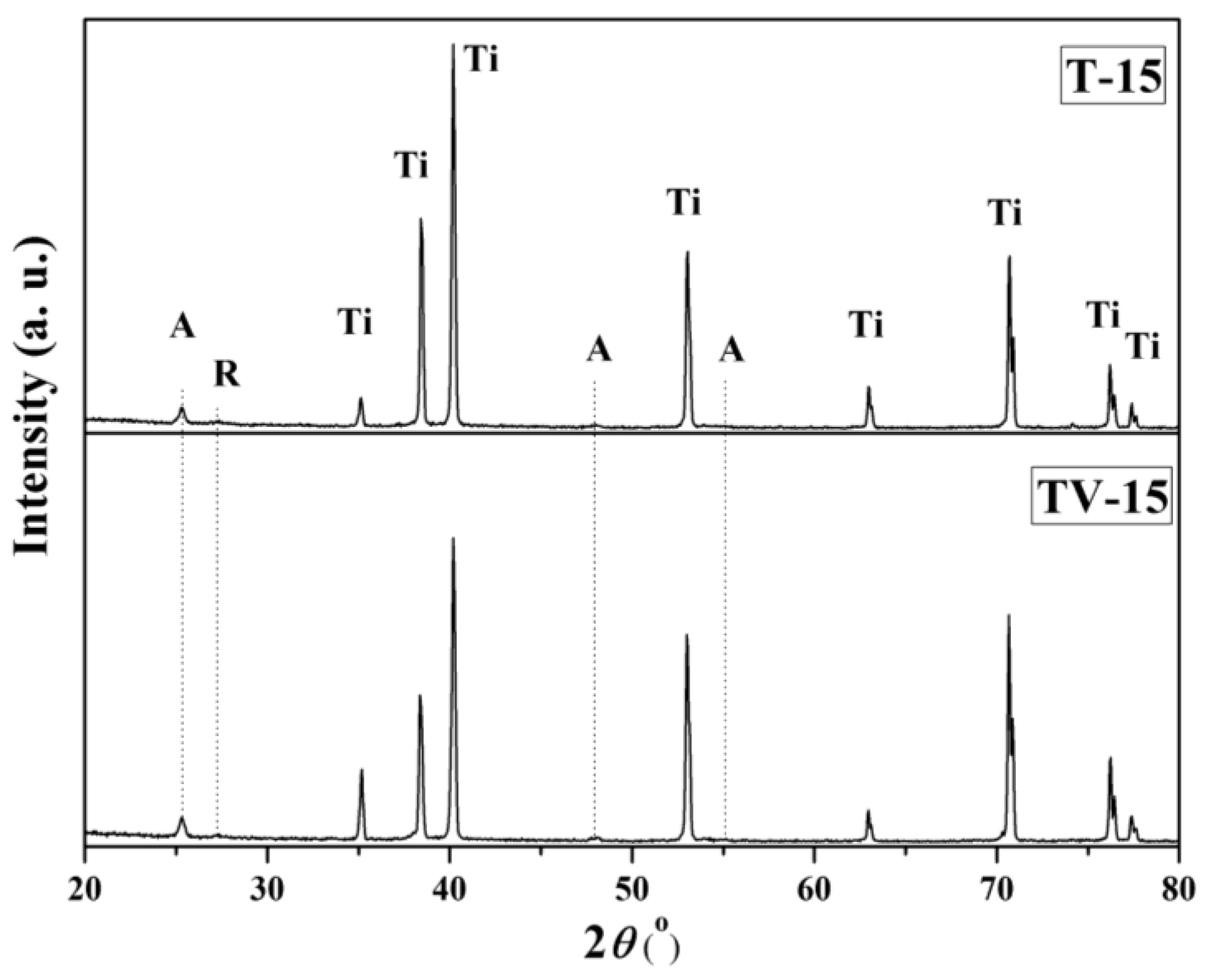
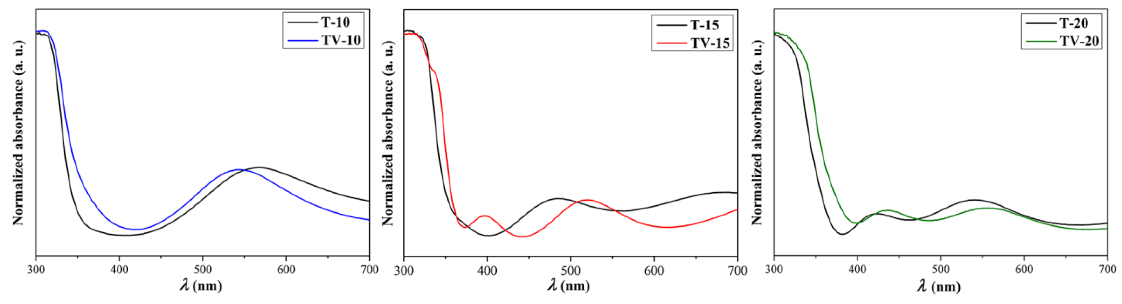
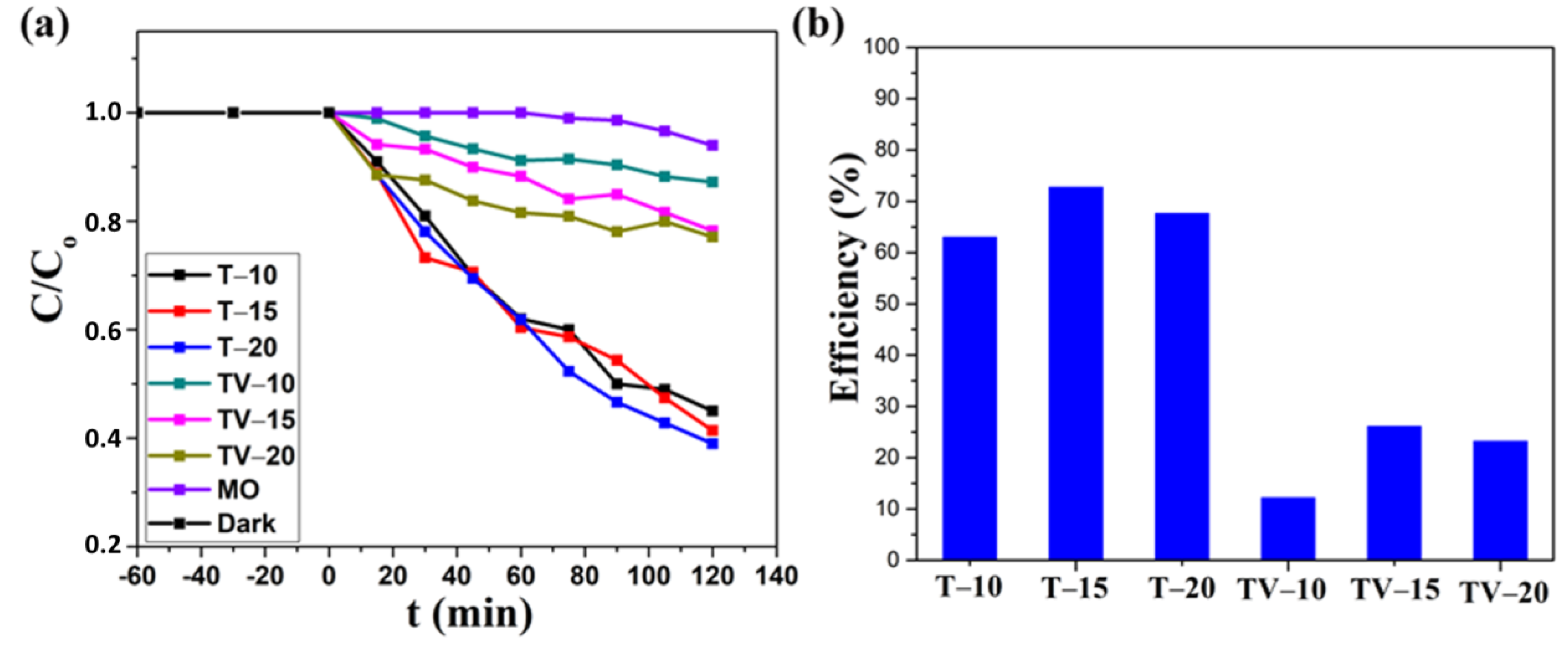
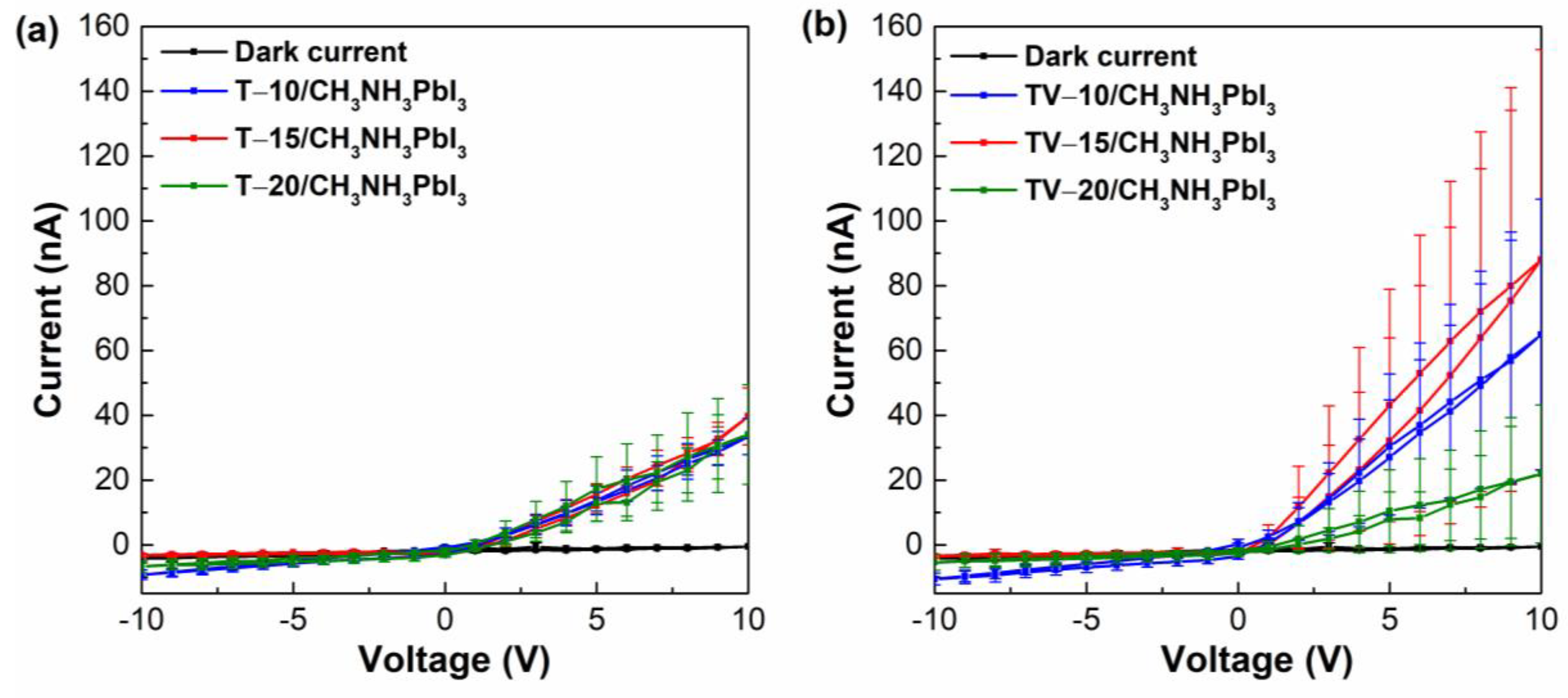
2. Results and Discussion

The influence of anodization voltage on the morphology of TiO2 nanotubes was investigated using SEM (Figure 1a–c). Well-aligned self-organized nanotube arrays were observed for anodization voltages from 10 to 20 V, and the diameter of the nanotubes increased with increasing voltage. Values of the microstructural parameters (statistical analysis results) are shown in Table 1. As the voltage increased from 10 V to 20 V, the outer diameter of nanotubes increased from ~62 nm to ~114 nm, while the wall thickness increased from ~8 nm to ~12 nm.
At a higher voltage (25 V), nanotubes were not produced, because the aqueous solution of HF used did not perform well, unlike organic electrolytes (based on ethylene glycol or glycerin), which allow voltages of up to 150 V [9,24]. On the other hand, voltages below 10 V in HF electrolytes lead to pore formation, without nanotubes [9].
Vanadium oxide was deposited on nanotubes synthesized at voltages from 10 to 20 V, and micrographs of samples are shown in Figure 1d–f, while morphological parameters of the samples are shown in Table 1. Although there is a slight increase in wall thickness and outer diameter of nanotubes with vanadium oxide deposition, this is within the range of the standard deviation. Cross-sections of samples without and with deposition of vanadium oxide are shown in Figure 2. The length of nanotubes increases from around 160 nm at 10 V, to 260–300 nm at 15 and 20 V.
The chemical composition of the surface after vanadium oxide deposition was examined using X-ray photoelectron spectroscopy (XPS). Survey XPS spectra consist of typical peaks for TiO2 (Ti and O) with the addition of a vanadium peak (Figure S1). The high-resolution spectra of these three peaks are presented in Figure 3. The positions of the Ti 2p3/2 peak for all three TV samples are 458.8 or 458.9 eV, while the positions of the Ti 2p1/2 peak are 464.6 or 464.7 eV. These confirm the presence of Ti4+ state in the TiO2 lattice [25]. The positions of Ti 2p peaks in the samples without vanadium oxide are at about the same energies, indicating that the deposition of vanadium oxide did not affect the valence state of titanium. After fitting the XPS spectrum of the O 1s line for TV samples, two contributions are observed. The main contribution is positioned at 530.2 eV and corresponds to O2− ions in the crystal lattice of TiO2 and vanadium oxide (Olatt—lattice oxygen). The other contribution, around 531.5–531.6 eV, can be attributed to the existence of oxygen species on the surface of the sample—Oads (possibly weakly bound oxygen, or a hydroxyl group) [26,27] and/or to subsurface low-coordinated oxygen ions O, where the latter exhibits lower electron density and, consequently, higher covalence of the M-O bonds (M: Ti, V) compared to classical O2− ions [28,29,30].
The chemical compositions of the samples are listed in Table 2 obtained by XPS. The positions of the O 1s peaks in TV samples were shifted towards higher values of the binding energy (by ≤ 0.2 eV), compared to the T-samples. The vanadium peak is observed only in samples on which vanadium oxide is deposited. The binding energy for V 2p3/2 is in the range 517.0–517.2 eV, while the values for V 2p1/2 are in the range 524.3–524.8 eV. The positions of the V 2p peaks correspond to the vanadium (V) state, indicating that the vanadium (IV) in the precursor oxidized after drying at 100 °C in air [31]. TV-10 and TV-15 contained the same concentration of vanadium, while the vanadium content was lower in TV-20 (Table 2).
Diffractograms of samples T-15 and TV-15 are shown in Figure 4. The most intensive peaks in T-15 originate from the titanium substrate (titanium plate) because the TiO2 film was thin (<300 nm). In addition, three anatase peaks (at 25°, 48°, and 55°) and a very weak peak on 27.3° corresponding to rutile are observed. The TV-15 diffractogram also shows peaks of titanium, anatase, and rutile. Anatase and rutile peaks do not exhibit any shift compared to the T-15. The crystalline sizes were estimated using Scherrer’s equation, and values of 20 and 22 nm were obtained for samples without and with vanadium oxide, respectively. The lack of changes in diffractograms is probably due to the small amount of vanadium oxide deposited on the nanotubes [26].
The influence of anodizing voltage on the optical properties of TiO2 nanotubes was examined with a UV-Vis spectrophotometer. The results for T-samples show that as the anodizing voltage increases, the absorbance shifts towards longer wavelengths (redshift) (Figure 5). Since the diameter and length of the nanotubes increase with increasing voltage, it is likely that the morphological characteristics of the nanotubes affect the optical properties of TiO2. As the length of the nanotube increases, the absorption edge shifts to the visible part of the spectrum, due to the increase in the amount of TiO2 [32] and higher absorption of incident photons, which leads to more photogenerated electron–hole pairs [33]. As the diameter of the nanotubes decreases, there is an absorbance shift towards lower wavelengths, because nanotubes with smaller diameters reflect more incident light due to the higher average dielectric constant [34]. It can be observed that samples synthesized at 10 V result in two peaks, while for 15 and 20 V, three peaks can be observed. The first peak in the UV region is characteristic of the TiO2, corresponding to the transition of electrons from the O 2p orbital of the valence band to the Ti 3d orbital of the conduction band [35]. The other two observable peaks are in the visible part of the spectrum. The first, at about 400–500 nm, corresponds to the trapped holes, while the second, at about 550–650 nm, corresponds to the trapped electrons at the Ti4+ center. This phenomenon is explained by the existence of localized states in the bandgap in TiO2 nanotubes [32,36]. Other authors claim that the peaks in the visible part of the TiO2 spectrum originate from oxygen vacancies or trapped electrons on Ti3+ centers located 0.1–0.8 eV below the TiO2 conduction band [35].
After the deposition of vanadium oxide on the TiO2 nanotubes, a redshift is observed for all TV samples. Wang and co-workers also observed an improvement effect of light absorption after vaporization of TiO2 nanofibers with V2O5 [16]. They explain that heterostructure TiO2/V2O5 promotes an increased separation of charge carriers. When the heterostructure is formed, the conduction band and valence band of V2O5 lie above that of TiO2, which induces the concentration of electrons in the conduction band of TiO2 and holes in the valence band of V2O5. In that way, the charges are better separated, which decreases recombination and improves optical properties. On the other hand, Liu and co-workers [14] observed better optical properties in the UV and visible region of TiO2 on which the V2O5 layer was deposited due to oxygen vacancies formed during the synthesis process that may capture the electrons. The expected absorption peak of vanadium(V) oxide, around 500 nm, is not observed [37], probably due to the presence of the overlapping TiO2 peak at about 550 nm. The Kubelka–Munk model and Tauc plot were used to determine the band gap of the samples, as shown in Table S1. A decrease in the band gaps is also evident with increases in the voltage of anodization and with deposition of vanadium oxide.
To determine the influence of nanotube morphology and vanadium oxide deposition on the photocatalytic properties of TiO2 nanotubes, photocatalytic degradation of methyl orange dye was investigated. Figure 6a shows the normalized curve of photocatalytic decomposition of MO over time. The photocatalytic decoloration efficiency of pure TiO2 increases with increasing anodization voltage, which can be correlated with the changes in the morphology. The minimum thickness of TiO2 film required for photocatalysis is reported to be about 150 nm [38], and the photocatalytic activity increases with increasing nanotube length up to a certain value (about 5 μm) [7]. The photocatalytic activity also first increases and then decreases with the increasing inner diameter and with the increasing wall thickness due to the corresponding decrease in the active surface of the nanotubes. In addition, the amount of TiO2 per unit area decreases with increasing nanotube diameter, while as the height of the nanotubes increases, the amount of TiO2 increases [39], creating diverging effects of photocatalytic performance. All of these combine, so the efficiency begins to decline after reaching a certain nanotube geometry [7]. For this reason, the optimization of morphological characteristics of TiO2 nanotubes is extremely important for TiO2 photoactivity. The effects of the morphology of T-samples on photocatalytic properties are relatively modest, with an increase in efficiency from 55% to 63% in T-10 and T-20, respectively, with T-20 exhibiting the best performance.
After the deposition of vanadium oxide, the photocatalytic properties worsen, regardless of the observed redshift in the UV/VIS spectra (Figure 5). Mahendra et al. [40] doped TiO2 with vanadium hydrothermally and observed that the photocatalytic efficiency worsened compared to undoped TiO2, although the band gap for the V-TiO2 sample was reduced to 1.95 eV. There are two possible reasons for this outcome: the first one is the absence of Ti3+ on the surface of V-TiO2, which can easily react with oxygen to form some radical species and improve photocatalysis; the other one is the presence of bulk vanadium species on the surface of the TiO2, which covered the photoactive site. According to Table 1, the TV-10 has the shortest nanotubes and thinnest wall compared to TV-15 and TV-20, and lowest photocatalytic efficiency. It could be assumed that the vanadium oxide layer covers more active surface, etc., so more photoactive sites for the adsorption of the dye are blocked for the TV-10 sample than for TV-15 and TV-20. On the other hand, TV-15 had the same amount of vanadium oxide as TV-10 but different microstructural parameters, and more area was available for the adsorption of the dye [14]. TV-20 shows a similar performance to TV-15, demonstrating that it has a similar amount of available surface for adsorption. It should be kept in mind that photocatalysis can also be negatively affected by recombination, which probably increases with vanadium oxide deposition. Although the TV-20 sample contained a smaller amount of vanadium (0.72 at.%, XPS analysis) and a thicker wall of nanotubes, which meant that most of the active surface was free for adsorption, the efficiency was not improved compared to unmodified TiO2, probably due to increased recombination. It can be concluded that with the deposition of vanadium oxide, the photocatalytic efficiency decreased more or less, depending on the morphological parameters of the nanotubes.
Heterojunctions with a p-semiconductor were manufactured using films of T and TV samples and CH3NH3PbI3 single crystal. The current–voltage characteristic of the heterojunction shows typical diode-like properties. Moreover, the diodes were sensitive to visible light and functioned as photodiodes. Figure 7a shows the influence of nanotube morphology on the photodiode characteristics of these hetero-compounds. Although the T-15 samples showed slightly higher photocurrent than T-10 and T-20, their performance was within experimental error, indicating that the nanotube morphology did not significantly impact their photovoltaic performance. It has been reported that the length of nanotubes affects electrical conductivity and thus the intensity of the photocurrent, while the diameter of the nanotube has no significant effect [41]. However, in our samples, the nanotubes were probably too short (˂300 nm) to observe the influence of nanotube height.
After the deposition of vanadium oxide, significant differences in the photocurrent of the heterojunctions are observed (Figure 7b). TV-10 and TV-15 have shown higher photocurrent, as compared to the pristine titania nanotube samples. The TV-15 sample performed the best, while the TV-10 sample, with the same vanadium content as TV-15, had a significantly lower photocurrent than TV-15, indicating the effect of nanotube morphology on the deposition of vanadium oxide layer; significant differences between these two samples were also observed in optical and photocatalytic properties. TV-20 had the lowest photocurrent among all samples. Moreover, the error bars increased after the deposition of vanadium oxide, indicating that the vanadium content was not homogenous across the TiO2 nanotubes.
A literature review indicates that V2O5 improves the separation of charge carriers, which is why it was expected to improve the photocatalytic response of TiO2 [14]. Minić and co-workers observed that after the deposition of vanadium oxide nanolayer on TiO2 nanoparticles, the efficiency of the solar cell decreased by 40% [42], which was attributed to the formation of localized states that represent electron capture sites. In addition, photoactivity is probably affected by the thickness of the vanadium oxide film, which further depends on the wall thickness of the nanotubes. The predominance of V5+ ions in the epitaxial vanadium oxide film decreases with increasing film thickness, and the thicker vanadium oxide film behaves more as a V (IV) than as a V (V) layer, which adversely affects photoactivity [43]. However, the T-15 sample has a critical nanotube wall thickness, resulting in better vanadium oxide coverage. The nanotube wall thickness of the T-15 is optimal to maximize electron transport, but thin enough not to interfere with electron transport between the vanadium oxide layer and TiO2. When this critical size increases or decreases, efficiency decreases, either due to less thickness and fewer active centers on the surface or poorer transfer of electrons or because vanadium oxide begins to have more and more recombination sites at greater wall thickness. Therefore, based on the above results, we postulate that vanadium oxide decoration on anodized titania nanotubes is beneficial for improving the performance metrics of halide perovskite-based photodiodes, solar cells, and light-emitting devices prepared by dry-pressing, lamination, and evaporation techniques.

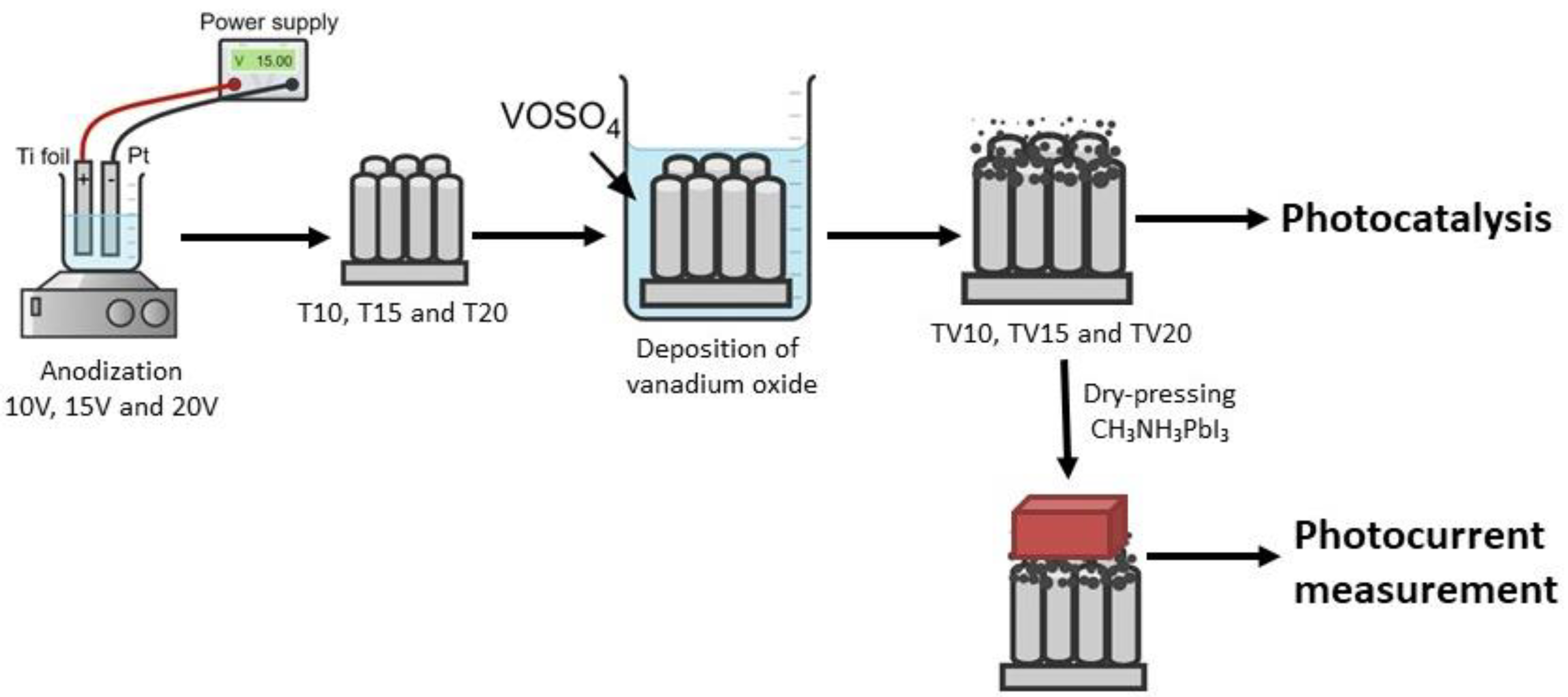
3. Materials and Methods

3.1. Synthesis of TiO2 Nanotubes

Highly ordered TiO2 nanotubes were synthesized by electrochemical oxidation of the titanium foils. To remove contamination, titanium foils were washed in acetone, ethanol, and water for 20 min in an ultrasonic bath. Subsequently, foils were rinsed with DI water and left to dry in the air. Degreased titanium foil was used as the anode, while a platinum foil was used as the cathode in the electrochemical configuration cell. The electrolyte consisted of 553 μL HF (40 mas.% in water, Centrohem, Stara Pazova, Serbia) and 252 μL CH3COOH (96%, Merck, Darmstadt, Germany) in 50 mL water. The titanium foils were anodized at different voltages: 10, 15, 20, and 25 V, for 30 min at room temperature. After anodization, samples were washed with DI water and dried in the air. Crystallization of the as-anodized TiO2 nanotubes was performed by annealing in the air for 30 min at 450 °C, with a heating speed of 5 °C/min. Samples were signed as T-10 (anodized at 10V), T-15 (anodized at 15 V), and T-20 (anodized at 20 V).

3.2. Deposition of Vanadium Oxide

To deposit vanadium oxide on TiO2 nanotube arrays, anodized titanium foils were soaked in an 0.01 M aqueous solution of VOSO4 (Sigma-Aldrich, St. Louis, MO, USA) for 2 min. Samples were dried in air at 100 °C, and then were assigned as TV-10, TV-15, and TV-20.

3.3. Synthesis of CH3NH3PbI3

CH3NH3PbI3 crystals were synthesized from the concentrated aqueous solution of hydroiodic acid (57 wt% in water, 99.99% Sigma-Aldrich, St. Louis, MO, USA), lead (II) acetate trihydrate (99.99%, Acros Organics, New Jersey, NY, USA), and a respective amount of a CH3NH2 solution (40 wt% in water, Sigma-Aldrich, St. Louis, MO, USA). A constant 55–42 °C temperature gradient was applied to induce the saturation of the solute at the low-temperature part of the solution [44].

3.4. Preparation of Heterojunction T-CH3NH3PbI3

Millimeter-sized single crystal CH3NH3PbI3 was dry-pressed against the top surfaces of T and TV samples. For electrical contacts, tungsten needles were used. One needle was contacted with the top part of the single crystal, while the other needle was placed on the titanium foil [23].
For a better understanding of synthesis methods, a graphical illustration is presented in Figure 8.

3.5. Characterization

The top view of the nanotubes was characterized by scanning electron microscopy (SEM, JOEL JSM-6390 LV, USA). To obtain a side view, the titanium foil was bent, and further characterization was performed by field emission scanning electron microscopy MIRA3 TESCAN (Czech Republic).
The elemental composition of the surface of the samples was determined using a Kratos Axis Ultra XPS system (Manchester, U.K.)with Monochromated Aluminum K-alpha X-Rays, where the X-Ray gun was operated at 15 kV and 10 mA. Pass energy for all surveys was 160 eV, while pass energy for all region scans was 20 eV. The samples were sputter-cleaned for 1 min before measurement. To reduce the charging effects from non-conducting surfaces, a charge neutralizer was used. All data were calibrated to the C-C portion of the C1s peak at 284.5 eV.
A Philips PW-1050 diffractometer was used to obtain the X-ray diffraction (XRD) patterns, which was operated at 40 kV and 30 mA, using Ni-filtered Cu Kα radiation (1.5419 Å). The patterns were taken in the 20–80° 2θ range with the step of 0.05° and collection time of 1 s per step.
The influence of the voltage of anodization and the VO deposition on optical properties of TNTs were measured by UV-Vis spectrophotometer Shimadzu UV-2600 (Japan).
For photocatalysis, a circle-shaped TiO2 film with a diameter of 1 cm was used as a photocatalyst. Based on the surface of the circle and the morphological parameters of the nanotube, the active surface area was calculated, i.e., available TiO2 surface for photocatalysis. The active surface area for photocatalysis was calculated by multiplying the number of nanotubes standing on the surface of 0.78 cm2 by the sum of areas of the outer shell, inner shell of the nanotubes and the surface of the upper side of the nanotubes (ring surface representing the wall thickness). The bottom surface of the nanotubes is neglected and is not included in the calculation of the active surface, because it represents a minor contribution and is unlikely to be accessible. The values of active areas are shown in Table 1. To be able to compare the photocatalytic activity of nanotubes of different morphologies, all photocatalytic activities were normalized to the active surface of T-10. The photocatalytic activity of samples (T and TV) was examined through the decomposition of methyl orange solution. Samples were immersed in 3 mL 5 M dye solution. Before photocatalytic measurement, samples were left in the solution for 1 h in the dark to obtain adsorption/desorption equilibrium. For illumination, a Hamamatsu spot light source LC8 was used with an intensity of 5.2 mW/cm2. The UV–visible absorption spectrum was recorded using a Varian Cary 50 Scan spectrophotometer to evaluate the photocatalytic performance. Besides photocatalytic activity, an investigation of the photolysis of MO was also performed. The photocatalytic activity was represented as C/C0 versus time of illumination (t), where C0 is initial dye concentration and C is dye concentration obtained after various interval of time.
The photocatalytic efficiency was calculated according to the equation:
E f f i c i e n c y = C 0 C 120 C 0   100   %
where C120 is the final dye concentration.
A Keithley 2400 source meter (Beaverton, OR, USA)was used for 2-point resistivity measurements (d.c.) to determine the devices current–voltage (I-V) characteristics. The voltage was swiped from 0 V to +10 V/−10 V and back with a scan speed of 1 V/s. Five different positions were tested on each foil, and the averages with respective errors were plotted in Figure 7. Fiberoptic-Heim LQ 1100 (intensity 1.83 mW/mm2) was used as a light source. All measurements were performed at room temperature, in an ambient atmosphere with 30% relative humidity.

4. Conclusions

TiO2 nanotubes were synthesized by anodizing titanium foil at 10 V, 15 V, and 20 V. After annealing in air, the samples were immersed in a vanadium (IV) precursor solution. XPS analysis proved that the precursor of vanadium, where vanadium was in the + IV oxidation state, oxidized after drying the samples at 100 °C in an air atmosphere and that vanadium(V) oxide was formed on the surface of the TiO2 nanotubes. Based on SEM micrographs, it was concluded that with increasing voltage from 10 V to 20 V, the diameter of nanotubes increases from 62 nm to 114 nm, while the wall thickness increases from 8 to 12 nm and the height of nanotubes from 160 nm to 300 nm. The increase in the height and diameter of the nanotubes influenced the appearance of the so-called redshift in the absorption spectrum and resulted in improved photocatalytic activity. The sample synthesized at 20 V showed the highest photocatalytic activity due to the optimal nanotube length and nanotube diameter. The presence of vanadium oxide on the surface of TiO2 nanotubes led to an additional redshift in the absorption spectrum, compared to nanotubes without a deposited vanadium oxide layer. However, regardless of the redshift in the absorption spectrum, there is a decrease in photocatalytic activity, probably due to the coating of the surface of the nanotubes for color adsorption, which worsens photocatalysis. To form an optoelectric device, a heterojunction between TNT/VO and CH3NH3PbI3 single crystals was formed. Measurements of current–voltage characteristics showed that nanotubes with a wall thickness of 10 nm and a height of about 260 nm show the highest value of photocurrent, due to adequate morphological parameters and the presence of 1.81 at% vanadium (V) on the surface of the nanotubes.

Supplementary Materials

The following supporting information can be downloaded at: https://www.mdpi.com/article/10.3390/catal13020352/s1, Figure S1: Survey XPS spectra of TiO2 nanotubes after vanadium oxide deposition; Table S1: Band gaps of the samples with and without vanadium oxide deposition.

Author Contributions

J.V.: investigation, analysis, original draft and writing—review and editing and visualization; P.A.: formal analysis and writing—review and editing; V.D.: formal analysis and writing—review and editing; V.B.: conceptualization, methodology, writing—review and editing; V.P.P.: formal analysis and writing—review and editing; J.Ć.: formal analysis and writing—review and editing; E.H.: conceptualization, writing—review and editing and supervision; L.F.: supervision; A.K.: formal analysis; V.B.P.: writing—review and editing and supervision; D.J.: writing—review and editing and supervision. All authors have read and agreed to the published version of the manuscript.

Funding

This research was supported by the projects provided by the Ministry of Education, Science and Technological Development of the Republic of Serbia (Record number: 451-03-68/2022-14/200175, 451-03-68/2022-14/200135, 451-03-68/2022-14/200105, and 451-03-68/2022-14/200116) and the National Science Foundation grants HRD-1345219 and DMR-1523617, and the Department of Energy/National Nuclear Security Administration NA0003979 award, and the Swiss National Science Foundation (No. 160169) and the ERC advanced grant “PICOPROP” (Grant No. 670918).

Institutional Review Board Statement

Not applicable.

Informed Consent Statement

Not applicable.

Data Availability Statement

Not applicable.

Acknowledgments

The authors further acknowledge Branislav Vlahović from North Carolina Central University, Department of Physics, USA.

Conflicts of Interest

The authors declare no conflict of interest.

References

  1. Shaikh, S.F.; Ghule, B.G.; Nakate, U.T.; Shinde, P.V.; Ekar, S.U.; O’Dwyer, C.; Kim, K.H.; Mane, R.S. Low-Temperature Ionic Layer Adsorption and Reaction Grown Anatase TiO2 Nanocrystalline Films for Efficient Perovskite Solar Cell and Gas Sensor Applications. Sci. Rep. 2018, 8, 11016. [Google Scholar] [CrossRef] [PubMed]
  2. Pérez-Jiménez, L.E.; Solis-Cortazar, J.C.; Rojas-Blanco, L.; Perez-Hernandez, G.; Martinez, O.S.; Palomera, R.C.; Paraguay-Delgado, F.; Zamudio-Torres, I.; Morales, E.R. Enhancement of Optoelectronic Properties of TiO2 Films Containing Pt Nanoparticles. Results Phys. 2019, 12, 1680–1685. [Google Scholar] [CrossRef]
  3. Djokić, V.R.; Marinković, A.D.; Petrović, R.D.; Ersen, O.; Zafeiratos, S.; Mitrić, M.; Ophus, C.; Radmilović, V.R.; Janaćković, D.T. Highly Active Rutile TiO2 Nanocrystalline Photocatalysts. ACS Appl. Mater. Interfaces 2020, 12, 33058–33068. [Google Scholar] [CrossRef]
  4. Cedillo-González, E.I.; Riccò, R.; Montorsi, M.; Montorsi, M.; Falcaro, P.; Siligardi, C. Self-Cleaning Glass Prepared from a Commercial TiO2 Nano-Dispersion and Its Photocatalytic Performance under Common Anthropogenic and Atmospheric Factors. Build. Env. 2014, 71, 7–14. [Google Scholar] [CrossRef]
  5. Miyoshi, A.; Nishioka, S.; Maeda, K. Water Splitting on Rutile TiO2-Based Photocatalysts. Chem. A Eur. J. 2018, 24, 18204–18219. [Google Scholar] [CrossRef]
  6. Pang, Y.L.; Lim, S.; Ong, H.C.; Chong, W.T. A Critical Review on the Recent Progress of Synthesizing Techniques and Fabrication of TiO2-Based Nanotubes Photocatalysts. Appl. Catal. A Gen. 2014, 481, 127–142. [Google Scholar] [CrossRef]
  7. Liu, B.; Nakata, K.; Liu, S.; Sakai, M.; Ochiai, T.; Murakami, T.; Takagi, K.; Fujishima, A. Theoretical Kinetic Analysis of Heterogeneous Photocatalysis by TiO2 Nanotube Arrays: The Effects of Nanotube Geometry on Photocatalytic Activity. J. Phys. Chem. C 2012, 116, 7471–7479. [Google Scholar] [CrossRef]
  8. Paramasivam, I.; Jha, H.; Liu, N.; Schmuki, P. A Review of Photocatalysis Using Self-Organized TiO2 Nanotubes and Other Ordered Oxide Nanostructures. Small 2012, 8, 3073–3103. [Google Scholar] [CrossRef] [PubMed]
  9. Mor, G.K.; Varghese, O.K.; Paulose, M.; Shankar, K.; Grimes, C.A. A Review on Highly Ordered, Vertically Oriented TiO2 Nanotube Arrays: Fabrication, Material Properties, and Solar Energy Applications. Sol. Energy Mater. Sol. Cells 2006, 90, 2011–2075. [Google Scholar] [CrossRef]
  10. Liu, Z.; Wang, B.; Wu, J.; Dong, Q.; Zhang, X.; Xu, H. Effects of Hydroxylation on PbS Quantum Dot Sensitized TiO2 Nanotube Array Photoelectrodes. Electrochim. Acta 2016, 187, 480–487. [Google Scholar] [CrossRef]
  11. de Brito, J.F.; Tavella, F.; Genovese, C.; Ampelli, C.; Zanoni, M.V.B.; Centi, G.; Perathoner, S. Role of CuO in the Modification of the Photocatalytic Water Splitting Behavior of TiO2 Nanotube Thin Films. Appl. Catal. B 2018, 224, 136–145. [Google Scholar] [CrossRef]
  12. Zeng, W.; Liu, X.; Wang, H.; Cui, D.; Xia, R.; Min, Y. Mechanism Study on Enhanced Open-Circuit Voltage of Perovskite Solar Cells with Vapor-Induced TiO2 as Electron-Transport Layer. Thin Solid Film. 2017, 629, 11–16. [Google Scholar] [CrossRef]
  13. Xu, J.; Zhang, T. Fabrication of Spent FCC Catalyst Composites by Loaded V2O5 and TiO2 and Their Comparative Photocatalytic Activities. Sci. Rep. 2019, 9, 11099. [Google Scholar] [CrossRef] [PubMed]
  14. Liu, Y.; Wang, L.; Jin, W.; Zhang, C.; Zhou, M.; Chen, W. Synthesis and Photocatalytic Property of TiO2@V2O5 Core-Shell Hollow Porous Microspheres towards Gaseous Benzene. J. Alloys Compd. 2017, 690, 604–611. [Google Scholar] [CrossRef]
  15. Epifani, M.; Chávez-Capilla, T.; Andreu, T.; Arbiol, J.; Palma, J.; Morante, J.R.; Díaz, R. Surface Modification of Metal Oxide Nanocrystals for Improved Supercapacitors. Energy Env. Sci 2012, 5, 7555. [Google Scholar] [CrossRef]
  16. Wang, Y.; Su, Y.R.; Qiao, L.; Liu, L.X.; Su, Q.; Zhu, C.Q.; Liu, X.Q. Synthesis of One-Dimensional TiO2/V2O5 Branched Heterostructures and Their Visible Light Photocatalytic Activity towards Rhodamine B. Nanotechnology 2011, 22, 225702. [Google Scholar] [CrossRef] [PubMed]
  17. Klosek, S.; Raftery, D. Visible Light Driven V-Doped TiO2 Photocatalyst and Its Photooxidation of Ethanol. J. Phys. Chem. B 2001, 105, 2815–2819. [Google Scholar] [CrossRef]
  18. Fan, J.; Jia, B.; Gu, M. Perovskite-Based Low-Cost and High-Efficiency Hybrid Halide Solar Cells. Photonics Res. 2014, 2, 111–120. [Google Scholar] [CrossRef]
  19. Zhu, Y.; Liu, Y.; Miller, K.A.; Zhu, H.; Egap, E. Lead Halide Perovskite Nanocrystals as Photocatalysts for PET-RAFT Polymerization under Visible and Near-Infrared Irradiation. ACS Macro. Lett. 2020, 9, 725–730. [Google Scholar] [CrossRef]
  20. Xu, Y.-F.; Yang, M.-Z.; Chen, B.-X.; Wang, X.-D.; Chen, H.-Y.; Kuang, D.-B.; Su, C.-Y. A CsPbBr3 Perovskite Quantum Dot/Graphene Oxide Composite for Photocatalytic CO2 Reduction. J. Am. Chem. Soc. 2017, 139, 5660–5663. [Google Scholar] [CrossRef]
  21. Zhu, Y.; Liu, Y.; Ai, Q.; Gao, G.; Yuan, L.; Fang, Q.; Tian, X.; Zhang, X.; Egap, E.; Ajayan, P.M.; et al. In Situ Synthesis of Lead-Free Halide Perovskite–COF Nanocomposites as Photocatalysts for Photoinduced Polymerization in Both Organic and Aqueous Phases. ACS Mater. Lett. 2022, 4, 464–471. [Google Scholar] [CrossRef]
  22. Elseman, A.M.; Zaki, A.H.; Shalan, A.E.; Rashad, M.M.; Song, Q.L. TiO2 Nanotubes: An Advanced Electron Transport Material for Enhancing the Efficiency and Stability of Perovskite Solar Cells. Ind. Eng. Chem. Res. 2020, 59, 18549–18557. [Google Scholar] [CrossRef]
  23. Vujančević, J.; Andričević, P.; Bjelajac, A.; Đokić, V.; Popović, M.; Rakočević, Z.; Horváth, E.; Kollár, M.; Náfrádi, B.; Schiller, A.; et al. Dry-Pressed Anodized Titania Nanotube/CH3NH3PbI3 Single Crystal Heterojunctions: The Beneficial Role of N Doping. Ceram. Int. 2019, 45, 10013–10020. [Google Scholar] [CrossRef]
  24. Roy, P.; Berger, S.; Schmuki, P. TiO2 Nanotubes: Synthesis and Applications. Angew. Chem. Int. Ed. 2011, 50, 2904–2939. [Google Scholar] [CrossRef] [PubMed]
  25. Biesinger, M.C.; Lau, L.W.M.; Gerson, A.R.; Smart, R.S.C. Resolving Surface Chemical States in XPS Analysis of First Row Transition Metals, Oxides and Hydroxides: Sc, Ti, V, Cu and Zn. Appl Surf. Sci. 2010, 257, 887–898. [Google Scholar] [CrossRef]
  26. Zhu, X.; Chen, J.; Yu, X.; Zhu, X.; Gao, X.; Cen, K. Controllable Synthesis of Novel Hierarchical V2O5/TiO2 Nanofibers with Improved Acetone Oxidation Performance. RSC Adv. 2015, 5, 30416–30424. [Google Scholar] [CrossRef]
  27. Fan, Z.; Guo, H.; Fang, K.; Sun, Y. Efficient V2O5/TiO2 Composite Catalysts for Dimethoxymethane Synthesis from Methanol Selective Oxidation. RSC Adv. 2015, 5, 24795–24802. [Google Scholar] [CrossRef]
  28. Kruse, N.; Chenakin, S. XPS Characterization of Au/TiO2 Catalysts: Binding Energy Assessment and Irradiation Effects. Appl. Catal. A Gen. 2011, 391, 367–376. [Google Scholar] [CrossRef]
  29. Dupin, J.-C.; Gonbeau, D.; Vinatier, P.; Levasseur, A. Systematic XPS Studies of Metal Oxides, Hydroxides and Peroxides. Phys. Chem. Chem. Phys. 2000, 2, 1319–1324. [Google Scholar] [CrossRef]
  30. Liu, H.; Yang, W.; Ma, Y.; Cao, Y.; Yao, J.; Zhang, J.; Hu, T. Synthesis and Characterization of Titania Prepared by Using a Photoassisted Sol−Gel Method. Langmuir 2003, 19, 3001–3005. [Google Scholar] [CrossRef]
  31. Silversmit, G.; Depla, D.; Poelman, H.; Marin, G.B.; De Gryse, R. Determination of the V2p XPS Binding Energies for Different Vanadium Oxidation States (V5+ to V0+). J. Electron Spectros. Relat. Phenom. 2004, 135, 167–175. [Google Scholar] [CrossRef]
  32. Zhuang, H.-F.; Lin, C.-J.; Lai, Y.-K.; Sun, L.; Li, J. Some Critical Structure Factors of Titanium Oxide Nanotube Array in Its Photocatalytic Activity. Env. Sci. Technol. 2007, 41, 4735–4740. [Google Scholar] [CrossRef] [PubMed]
  33. Sun, Y.; Yan, K.-P. Effect of Anodization Voltage on Performance of TiO2 Nanotube Arrays for Hydrogen Generation in a Two-Compartment Photoelectrochemical Cell. Int J. Hydrog. Energy 2014, 39, 11368–11375. [Google Scholar] [CrossRef]
  34. Paulose, M.; Mor, G.K.; Varghese, O.K.; Shankar, K.; Grimes, C.A. Visible Light Photoelectrochemical and Water-Photoelectrolysis Properties of Titania Nanotube Arrays. J. Photochem. Photobiol. A Chem. 2006, 178, 8–15. [Google Scholar] [CrossRef]
  35. Mazierski, P.; Nadolna, J.; Lisowski, W.; Winiarski, M.J.; Gazda, M.; Nischk, M.; Klimczuk, T.; Zaleska-Medynska, A. Effect of Irradiation Intensity and Initial Pollutant Concentration on Gas Phase Photocatalytic Activity of TiO2 Nanotube Arrays. Catal. Today 2017, 284, 19–26. [Google Scholar] [CrossRef]
  36. Lai, Y.; Sun, L.; Chen, Y.; Zhuang, H.; Lin, C.; Chin, J.W. Effects of the Structure of TiO2 Nanotube Array on Ti Substrate on Its Photocatalytic Activity. J. Electrochem. Soc. 2006, 153, D123. [Google Scholar] [CrossRef]
  37. Liu, J.; Yang, R.; Li, S. Synthesis and Photocatalytic Activity of TiO2/V2O5 Composite Catalyst Doped with Rare Earth Ions. J. Rare Earths 2007, 25, 173–178. [Google Scholar] [CrossRef]
  38. Li, S.; Zhang, G.; Guo, D.; Yu, L.; Zhang, W. Anodization Fabrication of Highly Ordered TiO2 Nanotubes. J. Phys. Chem. C 2009, 113, 12759–12765. [Google Scholar] [CrossRef]
  39. Adán, C.; Marugán, J.; Sánchez, E.; Pablos, C.; van Grieken, R. Understanding the Effect of Morphology on the Photocatalytic Activity of TiO2 Nanotube Array Electrodes. Electrochim. Acta 2016, 191, 521–529. [Google Scholar] [CrossRef]
  40. Mahendra, I.P.; Huda, A.; Ngoc, H.M.; Nghia, P.T.; Wirjosentono, B. Investigation of TiO2 Doped with Nitrogen and Vanadium Using Hydrothermal / Sol-Gel Method and Its Application for Dyes Photodegradation. Arab J. Basic Appl. Sci. 2019, 26, 242–253. [Google Scholar] [CrossRef] [Green Version]
  41. Krbal, M.; Sopha, H.; Podzemna, V.; Das, S.; Prikryl, J.; Macak, J.M. TiO2 Nanotube/Chalcogenide-Based Photoelectrochemical Cell: Nanotube Diameter Dependence Study. J. Phys. Chem. C 2017, 121, 6065–6071. [Google Scholar] [CrossRef]
  42. Minić, D.M.; Vesce, L.; Minić, D.G.; Di Carlo, A.; Blagojević, V.A. Effect of Deposition of Vanadium Oxide Nanolayer on Performance of TiO2 Dye- Sensitized Solar Cell Electrode. In Proceedings of the 11th International Conference on Fundamental and Applied Aspects of Physical Chemistry, Society of Physical Chemists of Serbia, Belgrade, Serbia, 22–26 September 2012; pp. 324–326. [Google Scholar]
  43. Gao, W.; Altman, E.I. Growth and Structure of Vanadium Oxide on Anatase (1 0 1) Terraces. Surf. Sci. 2006, 600, 2572–2580. [Google Scholar] [CrossRef]
  44. Mettan, X.; Pisoni, R.; Matus, P.; Pisoni, A.; Jaćimović, J.; Náfrádi, B.; Spina, M.; Pavuna, D.; Forró, L.; Horváth, E. Tuning of the Thermoelectric Figure of Merit of CH3NH3MI3 (M═Pb,Sn) Photovoltaic Perovskites. J. Phys. Chem. C 2015, 119, 11506–11510. [Google Scholar] [CrossRef] [Green Version]
Figure 1. SEM micrographs of samples: (a) T-10, (b) T-15, (c) T-20, (d) TV-10, (e) TV-15 and (f) TV-20 (the scale bare in each image is 200 nm).
Catalysts 13 00352 g001
Figure 2. Cross-section of TiO2 nanotube arrays for samples: (a) T-10, (b)T-15, (c)T-20 (d) TV-10, (e) TV-15, (f) TV-20.
Catalysts 13 00352 g002
Figure 3. High-resolution XPS spectrums for Ti 2p, O 1s, and V2p for samples TV-10, TV-15, and TV-20.
Catalysts 13 00352 g003
Figure 4. Diffractograms of TiO2 nanotubes synthesized at 15 V, with and without vanadium oxide deposition.
Catalysts 13 00352 g004
Figure 5. Comparison of UV-Vis spectra of nanotubes with and without vanadium oxide deposition.
Catalysts 13 00352 g005
Figure 6. Photocatalytic activity (a) and efficiency (b) of decolorization MO by TiO2 nanotubes with and without vanadium oxide.
Catalysts 13 00352 g006
Figure 7. Photocurrent characteristic of heterojunctions of TiO2 nanotubes and CH3NH3PbI3 single crystals. (a) TiO2 nanotubes without deposition of vanadium oxide and (b) nanotubes with deposition of vanadium oxide.
Catalysts 13 00352 g007
Figure 8. Schema of the method of synthesis of TiO2 nanotubes, deposition of vanadium oxide and heterojunction formation with monocrystal CH3NH3PbI3.
Catalysts 13 00352 g008
Table 1. Microstructural parameters of TiO2 nanotubes with (TV) and without (T) vanadium oxide deposition with standard deviation in brackets.
SamplesWall Thickness
nm
Outer Diameter
nm
Surfaces
cm2
SamplesWall Thickness
nm
Outer Diameter
nm
Surfaces
cm2
T-108 (2)62 (8)14.3TV-109 (2)63 (8)13.4
T-159 (2)93 (14)16.6TV-1510 (2)89 (12)17.1
T-2012 (3)114 (15)15.0TV-2012 (3)114 (14)15.0
Table 2. Chemical analysis of TiO2 nanotubes with and without vanadium oxide deposition.
SamplesTi
at.%
O
at.%
V
at.%
T-1018.949.30
T-1520.551.60
T-2019.648.90
TV-1016.250.61.8
TV-1516.549.81.8
TV-2017.149.10.7
Disclaimer/Publisher’s Note: The statements, opinions and data contained in all publications are solely those of the individual author(s) and contributor(s) and not of MDPI and/or the editor(s). MDPI and/or the editor(s) disclaim responsibility for any injury to people or property resulting from any ideas, methods, instructions or products referred to in the content.

