Article

Nanostructured Magnéli-Phase W18O49 Thin Films for Photoelectrochemical Water Splitting

1
Physics Department, King Fahd University of Petroleum and Minerals, Dhahran 31261, Saudi Arabia
2
Center of Research Excellence in Nanotechnology (CENT), King Fahd University of Petroleum and Minerals, Dhahran 31261, Saudi Arabia
*
Author to whom correspondence should be addressed.
Catalysts 2020, 10(5), 526; https://doi.org/10.3390/catal10050526
Submission received: 18 April 2020 / Revised: 4 May 2020 / Accepted: 8 May 2020 / Published: 10 May 2020
(This article belongs to the Special Issue Commemorative Issue in Honor of Professor Hugo de Lasa)

Abstract

:
Converting water into hydrogen through the photo-electrochemical (PEC) process is one of the most exciting approaches in this field, and there is a quest to design or search for new electro-photo-catalytic materials. In this work, simple steps for fabrication and transformation of metallic tungsten thin film into the photo-active Magnéli-phase (W18O49) of tungsten oxide thin film is demonstrated. The post-annealing temperature has a significant impact on the phase evolution of tungsten film into W18O49. The film thickness of W18O49 is controlled by controlling the sputtering time (or deposition time) of W film. The PEC performance of the as-prepared electrodes is evaluated by monitoring the water oxidation reaction under visible radiation. The PEC findings reveal a correlation between PEC performance and phase, morphology, and thickness of the film. The as-derived W18O49 can efficiently catalyze the water oxidation reaction at neutral solution pH, generating 0.6 and 1.4 mA cm−1 photo-current at 0.6 and 0.8 V vs. Saturated calomel electrode (SCE), respectively, in addition to excellent stability. The electrical conductivity and the charge transfer kinetics are investigated employing the electrochemical impedance spectroscopic (EIS) technique.

Graphical Abstract

1. Introduction

Strong overuse and dependence of fossil fuels (coal, oil, and natural gas) are intensifying air pollution and climate change. Water splitting is one of the most promising methods to generate clean energy through hydrogen and oxygen evolution reactions using a clean and sustainable approach. However, developing low-cost water-splitting catalysts is still a scientific challenge to generating chemicals and renewable fuels from different renewable feedstocks [1,2,3]. Photo-electrochemical (PEC) is a process of splitting water into its two constituents, oxygen and hydrogen, using solar power [4,5,6].
To date, several different semiconductor metal oxides such as ZnO, TiO2, CuO, Bi2WO6, and MoO3 have been developed for water splitting [7,8,9,10,11]. Among them, tungsten oxide is one of the most common semiconductor oxides used in PEC cells due to its ability to absorb the visible light spectrum, high stability in the electrolyte solutions, and the ability to exist in various compositional forms such as WO2, WO3, and W18O49 [12,13,14]. Additionally, the tungsten oxide valance band potential edge is much higher (3.2 eV) than the potential required to oxidize the water (1.23 eV) [15,16].
The Magnéli-phase (W18O49) [17], which is attracting considerable interest in different applications, such as solar cells, photo-catalysis, and sensors, is a non-stoichiometric tungsten oxide phase that possesses abundant oxygen vacancies [18,19]. The oxygen vacancies present in W18O49 is functionalized as active sites to enhance the adsorption of oxygen molecules from the water [18]. Moreover, the W18O49 phase is capable of absorbing visible light illumination, without the addition of other dopant materials [20,21].
The photo-catalytic activity of Magnéli-phase W18O49 is dictated by several factors, such as morphology, particle size, and surface area, which are ultimately controlled by the fabrication method. For example, Chongshen et al. [22] demonstrated that the light absorption properties of the W18O49 changed with changing the bulk W18O49 to nanorods, nanograins, nanofibers, and nanoparticles. Guojuan et al. [23] found that the directional growth of W18O49 significantly affected oxygen vacancies, bandgap width, electron/hole separation, and optical attributes.
Herein, we demonstrate the preparation of W18O49 thin films by annealing the metallic films of tungsten prepared by direct current (DC) sputtering. Formation of W18O49 thin films are optimized by changing the sputtering deposition time (and hence the film’s thickness), and varying the annealing temperature. The PEC performance of the as-obtained W18O49 thin films is investigated by monitoring the water oxidation reaction. The crystallinity, morphological features, oxidation state, oxygen vacancy, and charge transfer resistance of the fabricated films are determined and correlated to PEC performance.

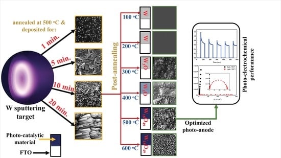
2. Results and Discussion

Figure 1 shows the X-ray diffraction (XRD) patterns of the sputtered W film and W18O49 films prepared under different conditions. The diffraction patterns of the W18O49 films synthesized by post-annealing of sputtered W films are presented in Figure 1a. As can be observed, the XRD of films prepared after different deposition time shows sharp reflections at 26.8°, 34.1°, 38.1°, 51.8°, and 54.8°, which are attributed to FTO glass substrate. Furthermore, the diffractions centered at 23.5°, 24.0°, 24.6°, 28.9°, 33.5°, and 34.0° are ascribed to (010), (502), (103), (004), (113), and (505) planes of monoclinic W18O49 with P2/m space group (JCPDS No: 84-1516) [24]. With increasing film thickness (deposition time), the intensity of the characteristic diffractions of W18O49 is increasing. The enhancement of the crystallinity by increasing the thickness of the film might be due to the energy of the impinging nanoparticle [25].
Figure 1b shows the phase evolution from W to W18O49 as a function of annealing temperature. As can be seen, the diffractions of the as-fabricated w film and those annealed at 100 °C and 200 °C show the patterns of the FTO substrate only, indicating the amorphous nature of the deposited films at these annealing temperatures. As the temperature was increased to 400 °C, the change of the amorphous to the crystalline phase is demonstrated by the appearance of the diffractions at 35.8°, 40.3°, and 44.1°. These reflections are attributed to (002), (110), and (112) planes of the W3O phase with Pm-3n space group (JCPDS No: 41-1230) [26]. Formation of W18O49 was observed at a higher temperature; the diffraction peaks of W film annealed at 500 and 600 °C matches the monoclinic phase of W18O49, indicating the phase transformation from W3O to W18O49 thin film. Thermal treatment of the W3O films in the air provides further oxygen molecules that are needed for the formation of W18O49. It is worth mentioning that no other diffraction peak appeared after the thermal heating procedures.
The surface morphologies of the fabricated films were investigated in detail by field-emission scanning electron microscopy (FE-SEM). FE-SEM images of the W18O49 films obtained after the post-annealing of sputtered W films prepared as a function of deposition time are shown in Figure 2. It can be observed that the thinnest film, deposited for 1 min, has a film thickness of 52 nm (Figure 2a,e), and it is originally grown in the form of packed spherical grains that have an average grain size ranging between 20 and 40 nm, numerous large particles with an average size of 70 nm, and small sheets. The diameter and length of these sheets are measured to be about 20 nm and 1.5 μm, respectively. Upon increasing the deposition time to 5 min, Figure 2b,f, the flat and compact surface of the W18O49 film evolved into a film with a thickness of 146 nm that attached as various large sheets over several micrometers. This transformation may be due to the formation of planar defects induced by the structural strain caused by heat treatment followed by aggregation process. The film deposited for 10 min has a thickness of 290 nm, as shown in Figure 2c,g. It consists of well-distributed and interconnected nanosized sheets without any significant voids. Meanwhile, W18O49 film deposited for 20 min shows uniform and stacked sheets to form a nanorod-like structure with a thickness of 550 nm, as shown in Figure 2d,h.
Low and high-magnification FE-SEM images of the sputtered W films annealed at different temperatures are shown in Figure 3. It can be noticed from Figure 3 that the microstructure of the films annealed at 100 °C and 200 °C revealed a compact, voids-free and smooth microstructure with small grains. At 300 °C, the deposited film started to crack, forming a first oxide phase (W3O) as a result of particles accumulation. With further heating, the particles built-up to form small sheets as shown in the samples annealed at 400 °C. At 500 °C, all the nanoparticles accumulated in groups to form uniform W18O49 nanosheets. By increasing the annealing temperature to 600 °C, the W18O49 nanosheets grew vertically to form a pillar-like structure as shown in the high-resolution inset image of 600 °C annealed sample.
The optical properties of the fabricated films are presented in Figure 4. Figure 4a shows the influence of W18O49 film’s thickness on the ability to absorb the light in the visible and ultraviolet (UV) range. As can be seen, the light absorption increased with increasing the deposition time of the films in both visible and UV range. This behavior is due to the increase in the average particle size caused by the increase of the W mass thickness. Furthermore, the absorption edge of W18O49 films shifted to a shorter wavelength (blue shift) when increasing the deposition time, which can presumably be ascribed to the quantum size effect. The optical band gap of the prepared photo-anodes is calculated using the Tauc relation [27,28]:
( α h v ) n = A ( h v E g )
where, α is the absorption coefficient, (Eg) is the optical band gap, h is the Planck’s constant, ν is the frequency, A is constant, n = 2 for direct bandgap and n = ½ for indirect bandgap. From Figure 4b, it was noticed that the bandgap decreases, from 3.65 eV (for 1 min film) to 3.18 eV (for 20 min film), as a result of increasing the thickness of the film, hence shifting its behavior from one dimension material to the bulk material. A similar shift in the bandgap of thin films induced by the variation of the thickness has been reported elsewhere [29]. Furthermore, annealing temperature also affected the optical properties of the W18O49 films. Films annealed at temperatures of 100 °C to 400 °C were opaque, indicating the metallic nature of the films while W18O49 film annealed at 500 °C and 600 °C (Figure 4c) showed a certain level of light absorption in the UV and visible range. Moreover, W18O49 film annealed at 600 °C showed a lower absorption level compared to the film annealed at 500 °C. This can be attributed to variation in the morphology of the two films as indicated by the FE-SEM images. The bandgap measurement plot of the W18O49 films annealed at 500 °C and 600 °C is shown in Figure 4d. The bandgap of W18O49 films annealed at 500 and 600 °C are calculated to be 3.45 and 3.50 eV. The value of bandgap slightly increased with increasing annealing temperature. This can presumably be due to the improvement in the crystallinity that resulted in the decrease of localized states in the bandgap [30].
The bonding and chemical environment of the deposited films was investigated by using X-ray photo-electron spectroscopy (XPS). Figure 5a,b show the XPS survey scans of the as-deposited W film and W18O49 film prepared at 500 °C. The results show the XPS spectra of W and O, confirming the high purity of the fabricated films. Moreover, the change in W 4f and O 1s peak intensities of these two films reveal the transformation of metallic W film to oxide phase. The de-convoluted peaks of W 4f XPS spectra show different chemical binding energies corresponding to different oxidation states, i.e., W° (W4f7/2 (31.1 eV), W4f5/2 (32.9 eV)), W5+ (W4f7/2 (35.0 eV) W6+ (W4f7/2 (35.0 eV), W4f5/2 (37.1 eV)) and Wx+ (W4f7/2 (eV), W4f5/2 (eV), which is an intermediate oxidation state between W° and W4+ [31,32]. Figure 5c demonstrates the W 4f spectra of as-grown W film, which shows the doublet peaks W 4f7/2 and W 4f5/2 formed due to the spin-orbit coupling. The presence of the small peaks at 31.6 and 33.8 eV is assigned to Wx+ such as W3O. The XPS spectrum of the prepared W18O49 thin film is displayed in Figure 5d. The W 4f peaks of the W18O49 films are shifted toward higher binding energy, compared with the W 4f spectra of the as-deposited film, which confirms the formation of the high oxidation state of W (5+, and 6+) [33,34]. The high-resolution XPS spectra of O 1s peaks of the as-fabricated sputtered W and W18O49 films are demonstrated in Figure 5e,f. The decomposition of the O1s peaks showed two different peaks at 530.5 and 532.3 eV which correspond to the lattice oxygen (OL) and oxygen vacancy (OV), respectively [35].
The PEC performance of the fabricated W18O49 photo-anode films was evaluated in 0.1 M of Na2SO4 electrolyte under the illumination of a 300 W Xenon lamp. Figure 6a shows the photo-current density generated by W18O49 films prepared at different deposition time at a bias 0.6 V. Under dark conditions, these samples did not produce any noticeable current. In the presence of light, photo-current was measured to be 0.10, 0.25, 0.60, and 0.62 mA/cm2 for W18O49 films deposited for 1, 5, 10, and 20 min, respectively. The weak photo-current recorded in the presence of W18O49 thin films deposited 1 and 2 min could be ascribed to the discontinuity of the film’s layer as indicated by FE-SEM images (Figure 2). The interconnected sheets of W18O49 film deposited for 10 min showed a significantly higher current density compared to the films prepared after shorter deposition time. This can be correlated to the lower bandgap (3.45 eV), and hence its ability to generate a larger number of electron/hole pairs. W18O49 deposited for 20 min generated comparable or a slightly higher photo-current than that of the film prepared after 10 min. A probable explanation can be as follows. All the photo-electrodes were illuminated from the front or coated side. The generated holes oxidize the water, while the electrons are transported to the counter electrode [36]. The photo-generated electrons have to diffuse through the entire film’s thickness to reach the FTO/W18O49 interface. In other words, the increase in film thickness after the optimal point enlarges the diffusion path for electrons and thus increases the probability of electron/hole pair recombination [37]. Potential-current curves obtained under intermittent illumination are shown in Figure 6b. The W18O49 films deposited for 10 and 20 min produced higher photo-current as compared to the films prepared after 1 and 5 min. It is noteworthy that no current was recorded under dark conditions even at high potential (0.8 V vs. SCE). The effect of annealing temperature on the PEC performance of W18O49 films is shown in Figure 6c. The potentiostatic measurements were carried out at 0.6 V vs. SCE. Since the as-prepared samples and those heated up to 300 °C (dashed line) were almost metallic, the production of low current was discerned under dark conditions. At 400 °C, the formation of W3O phase was observed, as confirmed by XRD and XPS. The film consisting of W3O layers was found to be photo-active and produced a photo-current of 0.4 mA/cm2. However, the generation of relatively high dark current was observed. The film obtained at 500 °C generated 0.6 mA/cm2. This film was formed in the shape of an interconnected nanosheet structure, which has high light absorption and high oxygen vacancies as confirmed by ultraviolet–visible (UV–Vis) and XPS results, respectively. These nanosheets were transformed into a nanopillar-like structure in the case of W18O49 prepared at 600 °C, resulting in reducing the absorbed light by the film, and hence, reducing its photo-current density to 0.3 mA/cm2. A similar trend was observed in the dark or light when linear sweep voltammetry (LSV) measurements were conducted at a voltage range from 0.25 to 0.80 V vs. SCE, Figure 6d. At low biased voltages, 0.0 to 0.20 V, 400 °C sample generated higher dark current, compared with 500 °C and 600 °C, due to its metallic nature (W3O phase).
The charge transfer process and electrical conductivity are very important factors in semiconductor photo-anode materials. Figure 7 shows EIS results obtained at 0.6 V vs. SCE at frequency ranging from 105 to 10−2 Hz in 0.1 M Na2SO4 electrolyte. Figure 7a shows the Nyquist plots (imaginary vs. real impedance) of W18O49 films deposited at different sputtering deposition times and annealing at 500 °C. All the experiments and measurements were carried out under illumination. One time constant circuit was used as equivalent circuit, in which, solution resistance (Rs) is connected in series with a sub-circuit formed of a capacitor connected in parallel with charge transfer resistance (Rct) [38]. It can be seen that the arc radiuses of the W18O49 films deposited for 20 min (Rct = 135 Ω) and 10 min (Rct = 172 Ω) were enormously short compared with 1 min (Rct = 760 KΩ) and 5 min (165 KΩ) W18O49 films, suggesting significantly faster charge transfer kinetics in the first mentioned W18O49 films [39]. This result was in good agreement with the PEC results. Nyquist plots of W films annealed at 300, 400, 500, and 600 °C were recorded under illumination and are shown in Figure 7b. The deposition time for all the film was 10 min. The Rct of photo-active materials prepared at 300, 400, 500, and 600 °C were measured to be 430, 240, 172, and 260 Ω, respectively. The surface charge resistance decreases with increasing calcination temperature from 300 to 500 °C, followed by an increase for the sample heated at 600 °C. The reduction in charge transfer resistance can be rationalized to the improvement in the crystallinity of the photo-catalysts, which increases with increase in calcination temperature. However, high calcination temperature, such as 600 °C, can also lead to sintering, change in morphology, and surface area of photo-catalytic materials. This notion was corroborated by microscopic analyses; the sheet morphology of the sample prepared at 500 °C was transformed into a nanopillar-like structure when heated at 600 °C. Such factors can undermine the photo-catalysts’ surface quality, which can affect the surface charge transfer negatively. For optimal performance, a balance between the crystallinity and other surface properties should be maintained. Charge transfer resistance of W18O49 film fabricated at 500 °C was also recorded with and without the light, and the results are shown in Figure 7c. It can be seen that in the absence of light, the Rct of the W18O49 film was significantly high (large semi-circle), which is in good agreement with the dark current shown in Figure 6c,d), and reflects the high photo-catalytic activity of W18O49 film. Figure 7d shows the stability of the photo-current density of W18O49 film deposited for 10 min and annealed at 500 °C at a biased voltage of 0.6 V vs. SCE under illumination. A slow drop was observed at the beginning (first 2000 s) due to the double layer charge capacitance at the W18O49 film/Na2SO4 interface [40]. After that, the photo-current density stabilizes at 0.56 mA/cm2, and it maintained 100% of this value for the 5200 s, which indicates the excellent stability of the photo-anode film.
Table 1 compares the photo-current density of the W18O49 film fabricated at 500 °C with those of other tungsten oxide photo-anodes, prepared by different methods. In this work, the fabricated photo-anode shows high photo-catalytic performance as compared to the most reported works in the table, indicating the high photo-catalytic activity of this phase and the effectiveness of the designed fabrication method.

3. Experimental Details

3.1. Preparation of W18O49 Thin-Film Electrodes

Tungsten oxide (W18O49) photo-anode films were fabricated by annealing the film of metallic tungsten prepared by the sputtering system (model NSC-4000, Nanomaster, TX, USA). Tungsten target (99.995% purity) was purchased from ACI alloys INC, (San Jose, CA, USA) and was used to deposit W films on FTO-coated glasses. The deposition was carried out in an argon atmosphere at a power of 100 watts. To investigate and reproduce the PEC performance of the W18O49, two films of each W18O49 were synthesized with varying thin-film thickness and post-annealing treatment. In both two parameters, the base and deposition pressure inside the sputtering chamber were fixed at 9 × 10⁻⁶ and 3.5 × 10⁻³ torr, respectively. To study the effect of the thin film thickness on the PEC activity of the W18O49, the sputtered W metallic films were deposited at varying thicknesses (1, 5, 10, and 20 min), while keeping all other parameters constant. To investigate the effect of post-annealing treatment on the performance of the W18O49, the sputtered W metallic films were annealed in a tube furnace (OTF-1200X from MTI corp.) at different temperatures in the ambient air. In detail, the deposited film was inserted in the middle of the tube furnace. Then, the furnace was adjusted to heat-up at the rate of 20 °C/min. to reach the targeted temperature (100, 200, 300, 400, 500, and 600 °C). After 2 h annealing, the tube furnace was switched off and the sample was left to cool down, inside the furnace in order to reach room temperature.

3.2. Thin Films’ Characterization

The fabricated photo-anode films were studded using different characterization techniques. The structural information and crystal phase of the fabricated films was investigated by X-ray diffraction (XRD, Rigaku Miniflex 600 X-ray Diffraction, Tokyo, Japan, with Cu K irradiation at λ = 1.5406 Å). The morphological properties were obtained using FE-SEM (Tescan Lyra-3, Brno-Kohoutovice, Czech Republic). The optical bandgap of the prepared films was calculated through ultraviolet and visible light absorption using an UV–Vis spectrophotometer (Jasco V-570, Tokyo, Japan). The subsurface composition was analyzed by X-ray photoelectron spectroscopy (XPS, Model: ESCALAB250Xi, Thermo Fisher, Waltham, MA, USA).

3.3. Evaluation of Photo-Electrochemical (PEC) Activity

The photo-electrochemical performance of the fabricated W18O49 photo-anode was carried out in a three-electrode cell connected to a potentiostat. In this assembly, W18O49 films, saturated calomel electrode (SCE; Hg/Hg2Cl2), and platinum coil were used as a working, reference, and counter electrodes, respectively. The photo-anodes were illuminated by a 300-watt Xenon lamp (Model: Max-303, Tokyo, Japan). The resistivity measurements of the fabricated electrodes were investigated by electrochemical impedance spectroscopy (EIS) in the frequency range of 10−2 to 105 Hz. All the above measurements were undertaken in 0.1 M of sodium sulfate (Na2SO4).

4. Conclusions

In summary, the study demonstrated the fabrication of tungsten metal film by a DC sputtering magnetron, and its transformation into Magnéli-phase (W18O49) thin film of tungsten oxide by post-annealing under an air environment. The thickness (52, 146, 290, and 550 nm) and the morphology (nanoparticles, nanosheets, nanorods, and nanopillars) of the thin films were controlled by adjusting film growth time and post-annealing process. The as-derived W18O49 efficiently catalyzed the water oxidation reaction and produced 0.6 and 1.4 mA cm−1 photo-current at 0.6 and 0.8 V vs. SCE, respectively. In addition, the photo-electrode showed excellent stability; the performance was stable for ~2 h. The electrical conductivity and the charge transfer kinetics were improved with increasing deposition time and post-annealing temperature. The photo-electrode with the lowest resistance exhibited the highest PEC performance.

Author Contributions

Conceptualization, A.K.M. and Q.A.D.; Formal analysis, Z.H.Y.; Investigation, A.K.M., Q.A.D. and Z.H.Y.; Methodology, A.K.M., Q.A.D. and M.Q.; Supervision, Z.H.Y.; Writing—original draft, A.K.M.; Writing—review & editing, Q.A.D., M.Q. and Z.H.Y. All authors have read and agreed to the published version of the manuscript.

Funding

This research was funded by the Deanship of Scientific Research (DSR) at King Fahd University of Petroleum & Minerals (KFUPM), grant number [No# DF181021].

Acknowledgments

The authors would like to acknowledge the support provided by the Deanship of Scientific Research (DSR) at King Fahd University of Petroleum & Minerals (KFUPM) for funding this work through project No# DF181021. The authors also acknowledge the Center of Excellence in Nanotechnology (CENT), King Fahd University of Petroleum and Minerals (KFUPM).

Conflicts of Interest

The authors declare no conflict of interest.

References

  1. Green, M.A. High-efficiency silicon solar cells. In Proceedings of the Seventh E.C. Photovoltaic Solar Energy Conference, Sevilla, Spain, 27–31 October 1986. [Google Scholar]
  2. Grimes, C.; Varghese, O.; Ranjan, S. Light, Water, Hydrogen: The Solar Generation of Hydrogen by Water Photoelectrolysis; Springer Science & Business Media: Berlin/Heidelberg, Germany, 2007. [Google Scholar]
  3. Eisenstadt, M.; Cox, K. Hydrogen production from solar energy. Sol. Energy 1975, 17, 59–65. [Google Scholar] [CrossRef]
  4. Çelik, D.; Yıldız, M. Investigation of hydrogen production methods in accordance with green chemistry principles. Int. J. Hydrog. Energy 2017, 42, 23395–23401. [Google Scholar] [CrossRef]
  5. Scott, K. Chapter 11. Conclusions: Electrolytic Hydrogen Production and Sustainable Routes. In Electrochemical Methods for Hydrogen Production; Royal Society of Chemistry: London, UK, 2019; Volume 25, pp. 392–404. [Google Scholar]
  6. Peter, L.M.; Wijayantha, K.G.U. Photoelectrochemical Water Splitting at Semiconductor Electrodes: Fundamental Problems and New Perspectives. Chem. Phys. Chem. 2014, 15, 1983–1995. [Google Scholar] [CrossRef] [PubMed]
  7. Zhang, X.; Qin, J.; Xue, Y.; Yu, P.; Zhang, B.; Wang, L.; Liu, R. Effect of aspect ratio and surface defects on the photocatalytic activity of ZnO nanorods. Sci. Rep. 2014, 4, 4596. [Google Scholar] [CrossRef] [Green Version]
  8. Weon, S.; Choi, W. TiO2 Nanotubes with Open Channels as Deactivation-Resistant Photocatalyst for the Degradation of Volatile Organic Compounds. Environ. Sci. Technol. 2016, 50, 2556–2563. [Google Scholar] [CrossRef]
  9. Artioli, G.A.; Mancini, A.; Barbieri, V.R.; Quattrini, M.C.; Quartarone, E.; Mozzati, M.C.; Drera, G.; Sangaletti, L.; Gombac, V.; Fornasiero, P.; et al. Correlation between Deposition Parameters and Hydrogen Production in CuO Nanostructured Thin Films. Langmuir 2016, 32, 1510–1520. [Google Scholar] [CrossRef]
  10. Bhattacharya, C.; Lee, H.C.; Bard, A.J. Rapid Screening by Scanning Electrochemical Microscopy (SECM) of Dopants for Bi2WO6 Improved Photocatalytic Water Oxidation with Zn Doping. J. Phys. Chem. C 2013, 117, 9633–9640. [Google Scholar] [CrossRef]
  11. Ma, C.; Zhou, J.; Zhu, H.; Yang, W.; Liu, J.; Wang, Y.; Zou, Z. Constructing a high-efficiency MoO3/polyimide hybrid photocatalyst based on strong interfacial interaction. ACS Appl. Mater. Interfaces 2015, 7, 14628–14637. [Google Scholar]
  12. Wu, M.; Lin, X.; Hagfeldt, A.; Ma, T. A novel catalyst of WO2 nanorod for the counter electrode of dye-sensitized solar cells. Chem. Commun. 2011, 47, 4535. [Google Scholar] [CrossRef]
  13. Liu, Y.; Wygant, B.R.; Kawashima, K.; Mabayoje, O.; Hong, T.E.; Lee, S.; Lin, J.; Kim, J.; Yubuta, K.; Li, W.; et al. Facet effect on the photoelectrochemical performance of a WO3/BiVO4 heterojunction photoanode. Appl. Catal. B Environ. 2019, 245, 227–239. [Google Scholar] [CrossRef]
  14. Zhang, N.; Jalil, A.; Wu, D.; Chen, S.; Liu, Y.; Gao, C.; Ye, W.; Qi, Z.; Ju, H.; Wang, C.; et al. Refining Defect States in W18O49 by Mo Doping: A Strategy for Tuning N2 Activation towards Solar-Driven Nitrogen Fixation. J. Am. Chem. Soc. 2018, 140, 9434–9443. [Google Scholar] [CrossRef] [PubMed]
  15. Seabold, J.A.; Choi, K.-S. Effect of a Cobalt-Based Oxygen Evolution Catalyst on the Stability and the Selectivity of Photo-Oxidation Reactions of a WO3 Photoanode. Chem. Mater. 2011, 23, 1105–1112. [Google Scholar] [CrossRef]
  16. Kudo, A.; Miseki, Y. Heterogeneous photocatalyst materials for water splitting. Chem. Soc. Rev. 2009, 38, 253–278. [Google Scholar] [CrossRef] [PubMed]
  17. Kieslich, G.; Tremel, W. Magnéli oxides as promising n-type thermoelectrics. AIMS Mater. Sci. 2014, 1, 184–190. [Google Scholar] [CrossRef]
  18. Bai, H.; Yi, W.; Liu, J.-Y.; Lv, Q.; Zhang, Q.; Ma, Q.; Yang, H.; Xi, G. Large-scale synthesis of ultrathin tungsten oxide nanowire networks: An efficient catalyst for aerobic oxidation of toluene to benzaldehyde under visible light. Nanoscale 2016, 8, 13545–13551. [Google Scholar] [CrossRef]
  19. Jia, C.; Zhang, X.; Matras-Postolek, K.; Huang, B.; Yang, P. Z-scheme reduced graphene oxide/TiO2-Bronze/W18O49 ternary heterostructure towards efficient full solar-spectrum photocatalysis. Carbon 2018, 139, 415–426. [Google Scholar] [CrossRef]
  20. Huang, Z.-F.; Song, J.; Pan, L.; Lv, F.; Wang, Q.; Zou, J.-J.; Zhang, X.; Wang, L. Mesoporous W18O49 hollow spheres as highly active photocatalysts. Chem. Commun. 2014, 50, 10959. [Google Scholar] [CrossRef]
  21. Guo, C.; Yin, S.; Huang, Y.; Dong, Q.; Sato, T. Synthesis of W18O49Nanorod via Ammonium Tungsten Oxide and Its Interesting Optical Properties. Langmuir 2011, 27, 12172–12178. [Google Scholar] [CrossRef]
  22. Guo, C.; Yin, S.; Yan, M.; Kobayashi, M.; Kakihana, M.; Sato, T. Morphology-Controlled Synthesis of W18O49 Nanostructures and Their Near-Infrared Absorption Properties. Inorg. Chem. 2012, 51, 4763–4771. [Google Scholar] [CrossRef]
  23. Hai, G.; Huang, J.; Jie, Y.; Cao, L.; Wang, L.; Fu, C.; Xiao, T.; Niu, M.; Feng, L. Unveiling the relationships between (010) facets-orientation growth and photocatalytic activity in W18O49 nanowires. J. Alloys Compd. 2020, 820, 153127. [Google Scholar] [CrossRef]
  24. Chen, P.; Qin, M.; Chen, Z.; Jia, B.; Qu, X. Solution combustion synthesis of nanosized WOx: Characterization, mechanism and excellent photocatalytic properties. RSC Adv. 2016, 6, 83101–83109. [Google Scholar] [CrossRef]
  25. Song, P.K.; Akao, H.; Kamei, M.; Shigesato, Y.; Yasui, I. Preparation and Crystallization of Tin-doped and Undoped Amorphous Indium Oxide Films Deposited by Sputtering. Jpn. J. Appl. Phys. 1999, 38, 5224–5226. [Google Scholar] [CrossRef]
  26. Maillé, L.; Sant, C.; Le Paven-Thivet, C.; Legrand-Buscema, C.; Garnier, P. Structure and morphological study of nanometer W and W3O thin films. Thin Solid Film. 2003, 428, 237–241. [Google Scholar] [CrossRef]
  27. Tauc, J. Optical Properties of Amorphous Semiconductors. In Amorphous and Liquid Semiconductors; Springer Science and Business Media LLC: Berlin/Heidelberg, Germany, 1974; pp. 159–220. [Google Scholar]
  28. Al-Kuhaili, M. Electromodulated transmittance of optical transitions in tungsten oxide. J. Phys. Chem. Solids 2020, 139, 109317. [Google Scholar] [CrossRef]
  29. Abdelrahman, A.; Yunus, W.; Arof, A.K. Optical properties of tin sulphide (SnS) thin film estimated from transmission spectra. J. Non Cryst. Solids 2012, 358, 1447–1451. [Google Scholar] [CrossRef]
  30. Vani, V.P.G.; Reddy, M.R.V.; Reddy, K.T.R. Influence of Source—Substrate Distance of Cu4SnS4 Thin Films Grown by Co-Evaporation. Adv. Mater. Res. 2013, 768, 103–108. [Google Scholar] [CrossRef]
  31. Wong, H.; Zhou, J.; Zhang, J.; Jin, H.; Kakushima, K.; Iwai, H. The interfaces of lanthanum oxide-based subnanometer EOT gate dielectrics. Nanoscale Res. Lett. 2014, 9, 472. [Google Scholar] [CrossRef] [Green Version]
  32. Xie, F.; Gong, L.; Liu, X.; Tao, Y.; Zhang, W.; Chen, S.; Meng, H.; Chen, J. XPS studies on surface reduction of tungsten oxide nanowire film by Ar+ bombardment. J. Electron Spectrosc. Relat. Phenom. 2012, 185, 112–118. [Google Scholar] [CrossRef]
  33. Zhong, Q.; Macharia, D.K.; Zhong, W.; Liu, Z.; Chen, Z. Synthesis of hydrophobic W18O49 nanorods for constructing UV/NIR-shielding and self-cleaning film. Ceram. Int. 2020. [Google Scholar] [CrossRef]
  34. Lv, Z.; Liu, H.; Zhang, X.; Shen, X.; Liu, S.; Wu, X.; Fang, M.; Liu, Y.-G.; Min, X.; Huang, Z. Solvothermally synthesized highly porous W18O49 nanowires for UV, humidity and pH detection. Phys. E Low Dimens. Syst. Nanostruct. 2020, 117, 113719. [Google Scholar] [CrossRef]
  35. Wang, J.; Chen, Z.; Zhai, G.; Men, Y. Boosting photocatalytic activity of WO3 nanorods with tailored surface oxygen vacancies for selective alcohol oxidations. Appl. Surf. Sci. 2018, 462, 760–771. [Google Scholar] [CrossRef]
  36. Park, Y.; McDonald, K.J.; Choi, K.-S. Progress in bismuth vanadate photoanodes for use in solar water oxidation. Chem. Soc. Rev. 2013, 42, 2321–2337. [Google Scholar] [CrossRef] [PubMed]
  37. Liu, X.; Zhou, H.; Pei, S.; Xie, S.; You, S. Oxygen-deficient WO3−x nanoplate array film photoanode for efficient photoelectrocatalytic water decontamination. Chem. Eng. J. 2020, 381, 122740. [Google Scholar] [CrossRef]
  38. Hosseini, M.G.; Sefidi, P.Y.; Aydin, Z.; Kinayyigit, S. Toward enhancing the photoelectrochemical water splitting efficiency of organic acid doped polyaniline-WO3 photoanode by photo-assisted electrochemically reduced graphene oxide. Electrochim. Acta 2020, 333, 135475. [Google Scholar] [CrossRef]
  39. Qamar, M.; Merzougui, B.; Ahmed, M.I.; Yamani, Z.H. Broad Solar Spectrum-Responsive and Highly Efficient Photoanode of Nonstoichiometric TiO2 Nanoplates/Reduced Graphene Oxide. ACS Sustain. Chem. Eng. 2017, 6, 2112–2121. [Google Scholar] [CrossRef]
  40. Mai, M.; Ma, X.; Zhou, H.; Ye, M.; Li, T.; Ke, S.; Lin, P.; Zeng, X. Effect of oxygen pressure on pulsed laser deposited WO3 thin films for photoelectrochemical water splitting. J. Alloys Compd. 2017, 722, 913–919. [Google Scholar] [CrossRef]
  41. Claudino, C.H.; Kuznetsova, M.; Rodrigues, B.S.; Chen, C.; Wang, Z.; Sardela, M.; Souza, J.S. Facile one-pot microwave-assisted synthesis of tungsten-doped BiVO4/WO3 heterojunctions with enhanced photocatalytic activity. Mater. Res. Bull. 2020, 125, 110783. [Google Scholar] [CrossRef]
  42. Wang, R.; Shen, J.; Zhang, W.; Liu, Q.; Zhang, M.; Zulfiqar; Tang, H. Build-in electric field induced step-scheme TiO2/W18O49 heterojunction for enhanced photocatalytic activity under visible-light irradiation. Ceram. Int. 2020, 46, 23–30. [Google Scholar] [CrossRef]
  43. Zhang, T.; Paulose, M.; Neupane, R.; Schaffer, L.A.; Rana, D.B.; Su, J.; Guo, L.; Varghese, O.K. Nanoporous WO3 films synthesized by tuning anodization conditions for photoelectrochemical water oxidation. Sol. Energy Mater. Sol. Cells 2020, 209, 110472. [Google Scholar] [CrossRef]
  44. Markhabayeva, A.A.; Moniruddin; Dupre, R.; Abdullin, K.A.; Nuraje, N. Designing of WO3@Co3O4 Heterostructures to Enhance Photoelectrochemical Performances. J. Phys. Chem. A 2019, 124, 486–491. [Google Scholar] [CrossRef]
  45. Zhao, L.-D.; Zhang, Q.; Fan, J.-B.; Yin, L.-Q.; Qi, P.-W.; Yao, H.-C.; Li, Z.-J. Improvement of the photoelectrochemical performance of vertically aligned WO3 nanosheet array film with a disordered surface layer by electroreduction. J. Solid State Electrochem. 2019, 23, 1621–1630. [Google Scholar] [CrossRef]
  46. Kalanur, S.S.; Seo, H. Aligned nanotriangles of tantalum doped tungsten oxide for improved photoelectrochemical water splitting. J. Alloys Compd. 2019, 785, 1097–1105. [Google Scholar] [CrossRef]
  47. Acosta, M.; Méndez, R.A.; Riech, I.; Rodríguez-Pérez, M.; Gattorno, G.R. Structural, optical and photoelectrochemical properties of tungsten oxide thin films grown by non-reactive RF-sputtering. Superlattices Microstruct. 2019, 127, 123–127. [Google Scholar] [CrossRef]
  48. Pedroni, M.; Canetti, M.; Chiarello, G.L.; Cremona, A.; Inzoli, F.; Luzzati, S.; Pietralunga, S.; Tagliaferri, A.; Zani, M.; Vassallo, E. Tungsten oxide thin film photo-anodes by reactive RF diode sputtering. Thin Solid Film. 2016, 616, 375–380. [Google Scholar] [CrossRef]
  49. Pedroni, M.; Chiarello, G.L.; Vassallo, E.; Selli, E. Multilayer WO3/BiVO4 Photoanodes for Solar-Driven Water Splitting Prepared by RF-Plasma Sputtering. Surfaces 2020, 3, 10. [Google Scholar] [CrossRef] [Green Version]
  50. Cole, B.; Marsen, B.; Miller, E.; Yan, Y.; To, B.; Jones, K.; Al-Jassim, M. Evaluation of Nitrogen Doping of Tungsten Oxide for Photoelectrochemical Water Splitting. J. Phys. Chem. C 2008, 112, 5213–5220. [Google Scholar] [CrossRef]
  51. Li, W.; Liu, C.; Yang, Y.; Li, J.; Chen, Q.; Liu, F. Platelike WO3 from hydrothermal RF sputtered tungsten thin films for photoelectrochemical water oxidation. Mater. Lett. 2012, 84, 41–43. [Google Scholar] [CrossRef]
  52. Valerini, D.; Hernández, S.; Di Benedetto, F.; Russo, N.; Saracco, G.; Rizzo, A. Sputtered WO3 films for water splitting applications. Mater. Sci. Semicond. Process. 2016, 42, 150–154. [Google Scholar] [CrossRef]
  53. Wiriyachailerd, C.; Horprathum, M.; Eiamchai, P.; Ponchio, C. Improved the chrage transfer for highly efficient photoelectrochemical water oxidation: The case of WO3 and BiVO4. Mater. Today Proc. 2018, 5, 13874–13878. [Google Scholar] [CrossRef]
Figure 1. X-ray diffraction (XRD) patterns of the (a) W18O49 films with various thickness fabricated by post-annealing of sputtered W film at 500 °C in air (b) metallic W film to W18O49 phase transformation as a function of post-annealing treatment.
Catalysts 10 00526 g001aCatalysts 10 00526 g001b
Figure 2. Field-emission scanning electron microscopy (FE-SEM) images of W18O49 films deposited for (a) 1, (b) 5, (c) 10, and (d) 20 min. and FE-SEM cross-section images of W18O49 films deposited for (e) 1, (f) 5, (g) 10, and (h) 20 min. All the films were annealed at 500 °C in air.
Catalysts 10 00526 g002
Figure 3. Low and high magnification FE-SEM images of the W films annealed at (a) 100, (b) 200, (c) 300, (d) 400, (e) 500, and (f) 600 °C in air.
Catalysts 10 00526 g003
Figure 4. Ultraviolet–visible (UV-Vis) absorption spectra and bandgap of W18O49 films as a function of deposition time (a,b), and UV-Vis absorption spectra and Tauc’s plot of W18O49 films (c,d) fabricated by post-annealing of sputtered W films at 500 and 600 °C in air.
Catalysts 10 00526 g004
Figure 5. X-ray photo-electron spectroscopy (XPS) spectra of (a,b) the survey spectra, (c,d) W4f, and (e,f) O1s of the as-deposited W film and W18O49 film fabricated at 500 °C, respectively.
Catalysts 10 00526 g005
Figure 6. Photo-electrochemical (PEC) performance measurements: Potentiostatic (a,c) and potentiodynamic (b,d) response of the films obtained at different deposition time and annealing temperatures. Measurements were carried out under intermittent light illumination.
Catalysts 10 00526 g006aCatalysts 10 00526 g006b
Figure 7. (a) Nyquist plots of W18O49 films deposited for 1, 5, 10, and 20 min under light. (b) Nyquist plots of W films annealed at 300, 400, 500, and 600 °C under light. (c) Nyquist plots of W18O49 films deposited for 10 min and annealed at 500 °C under dark and light. (d) Stability test of W18O49 films deposited for 10 min and annealed at 500 °C under light for 7200 s.
Catalysts 10 00526 g007
Table 1. A comparison between the optimized W18O49 film fabricated at 500 °C in air and different tungsten oxide photo-anodes reported in the literature.
Preparation MethodStructurePhoto-Current
mA/cm2
Bias VoltageElectrolyteLight SourceRef.
solvothermalplates-like0.200.6 V vs. Ag/AgCl0.5 M Na2SO4solar simulation
A.M. 1.5 G spectrum with the intensity of 100 mW·cm−2
[41]
solvothermalspindle-like0.20Ag/AgCl0.5 M Na2SO4-[42]
tungsten foil anodizationnanoporous layer0.400.6 V vs. Ag/AgCl0.5 M Na2SO4300 W Xe lamp[43]
Spin coatingNano particles0.251.25 V vs. RHE0.1 M Na2SO4300 W Xenon lamp[38]
electrodepositionNano-islands0.020.7 V vs. Ag/AgCl0.5 M H2SO4Xenon solar simulator (AM 1.5 G, 100 mW/cm2)[44]
hydrothermal methodNanosheets0.91.2 V vs. RHE0.5 M Na2SO4LED lamp coupled with an AM 1.5 G filter (100 mW cm−2, CEL-LED 100)[45]
hydrothermal methodNanosheets0.31.2 V vs. RHE0.5 M Na2SO41000 W xenon arc lamp[46]
RF-sputteringRough film0.011 V vs. Ag/AgCl1 M HClO4400 W ozone-free Xe arc lamp (AM 1.5 G filter)[47]
RF-sputteringfilm0.90.6 V vs. SCE0.5 M Na2SO4mercury arc lamp
350 nm < λ < 450 nm
[48]
RF-sputteringfilm0.30.6 V vs. SCE0.5 M Na2SO4300 W LOT-qd Xe lamp,
equipped with an AM 1.5 G filter
[49]
RF-sputtering Nanosheets<0.5 0.6 V vs. SCE0.33 molar H3POAM 1.5 G illumination generated by solar simulator[50]
RF-sputteringfilm0.20.6 V vs. Ag/AgCl0.5 mol/L H2SO4A 500 W Xe lamp/A 400 nm cutoff filter[51]
RF-sputteringfilm00.6 V vs. RHE0.1 M Na2SO4Xe lamp (150 W)/wavelengths range from 300 to 570 nm[52]
DC-sputteringfilm0.05 1.0 V vs. Ag/AgCl0.5 M Na2SO4visible light irradiation (λ > 420 nm)[53]
DC-sputteringNanosheets0.60.6 V vs. SCE0.5 M Na2SO4300 W Xenon lamp
UV-visible (300–600 nm)
This work
RHE: reversible hydrogen electrode, SCE: saturated calomel electrode, LED: light emitting diode.

