Article

The Impacts of Fluorine-Doped Tin Oxide Photonic Crystals on a Cadmium Sulfide-Based Photoelectrode for Improved Solar Energy Conversion under Lower Incidence

1
Institute of Semiconductors, South China Normal University, Guangzhou, Guangdong 510631, China
2
School of Chemistry, Faculty of Science, Chemistry Building F11, Camperdown 2050, University of Sydney, Sydney, NSW 2006, Australia
*
Authors to whom correspondence should be addressed.
These authors equally contributed to this work.
Catalysts 2020, 10(11), 1252; https://doi.org/10.3390/catal10111252
Submission received: 14 September 2020 / Revised: 4 October 2020 / Accepted: 9 October 2020 / Published: 29 October 2020
(This article belongs to the Special Issue Porous Materials for Photocatalysis and Energy)

Abstract

:
Incident angle variation of light from the sun is a critical factor for the practical utilizations of solar energy devices. These devices typically receive the zenith of photon density under a solar elevation angle of 90°, and dramatic deletion of light density along with the decrease of solar elevation angle. Photonic crystals (PCs) with long range ordered arrays possess the controllable position of the photonic stop band (PSB) reliant on several factors, including incident angles, based on the Bragg–Snell law. The multiple scattering, refraction and inhibition of charge carrier recombination within the PSB suggests the potential capability for improving the efficiency of photoactive materials. In this work, we focus on the multiple scattering and refraction effects of PCs. A photoelectrode based on photonic crystal fluorine-doped tin oxide (PC FTO) film was fabricated, which allows the embedded photoactive materials (CdS nanoparticles) to benefit from the features of PCs under variable incidence, especially under lower incidence. The photoelectrode thus has enhanced overall photoelectrochemical (PEC) efficiency in different seasons, even if the increased surface area factor is deducted.

1. Introduction

The performance of a PEC device is reliant on the optimization of light absorption, charge carrier separation and collection, catalysis and electrolyte/product diffusion [1,2]. Each of these factors would be affected by the geometry of the device and the morphology of the photoelectrode surface. With respect to a planar geometry, a photoelectrode with nano-structure typically presents increased electrolyte-electrode interface area and specific surface area available for loading photoactive materials. The effect on light absorption and charge separation is more complex. Charge separation will be dependent on charge recombination rates via control of the relative ratio of the structural dimensions and charge carrier diffusion lengths, and surface structure and defects [3,4,5]. Light capture will exhibit wavelength-dependent penetration depth, and morphology-dependent scattering and photonic effects, which can modify and even enhance light absorption [6]. Various ordered and amorphous structures have been prepared to investigate the effect of electrode structure, including porous, nanorod and nanoparticle morphologies to optimize photoelectrochemical performance [1,7,8,9,10,11,12].
Among many functional structures, PCs with long-range ordered periodic arrays possess the modulation of refractive index (RI) on the optical wavelength scale. The periodicity and the RI differences between external media (electrolyte, air, other materials, etc.) and PCs materials are predominant for the formation of PSB, light refraction and light scattering. Within the region of PSB or the PSB edge (commonly expressed as reflectance in visible wavelength), several photonic effects, including refraction, scattering, slow photon and suppression of recombination will fully or partially occur [13]. Among these photonic effects, the light refraction and scattering could occur under any circumstances, due to the 3D architecture and the RI differences of PCs. These would enhance the light harvesting of the embedded photoactive materials inside PCs, especially under lower incidences. Considering the practical utilizations, the photoelectrodes receive photons of varied incidences, due to the changing solar elevation of the sun. Typically, the light density would reach its zenith at summer noon of highest solar elevation (north earth). The light density being received by a planar photoelectrode would dramatically decrease under lower elevation angles.
Transparent conducting oxides (TCOs) exhibit a combination of transparency in the visible wavelength range and low resistivity and are used extensively in display and energy technologies, including low emissivity coatings, photovoltaics and photoelectrochemistry [14]. Doped metal oxides of In2O3, ZnO and SnO2 have all been intensively investigated and have a range of properties suited to individual applications. As the most commonly used TCO in photoelectrochemistry, tin doped indium oxide (ITO) is prone to reduction and highly transparent to visible light; however, the high cost and poor thermal stability [15] limit its applications. In comparison, although fluorine-doped tin oxide (FTO) typically exhibits greater resistivity than ITO, it is inexpensive and has high thermal stability and chemical stability in aqueous media [14]. Therefore, conductive PCs films of FTO would be a potentially attractive substrate for photoelectrochemical applications.
Recently, examples of structured FTO films have been reported. Disordered FTO spheres have been coated with TiO2 for a dye-sensitized solar cell application [15], and ordered arrays of nanopillars and nanocones have been used to support films of WO3 [16,17,18] and Ti:Fe2O3 [19,20]. PC FTO films supported on planar FTO have been prepared using polystyrene templating [21,22] and coated with TiO2 [23], WO3 [24] or BiWO4 [25] for PEC water oxidation under UV and visible light. These works were mainly focused on the massive surface area of PC FTO for supporting the PEC reactions. The integrated PEC performance of photoelectrode as a function of incident angle remains unexplored.
Herein, CdS as a photoactive material is directly loaded in PC FTO for the fabrication of the photoelectrode. Despite the increased surface area of PC FTO, the CdS/PC FTO performs with greater photocurrent density under angles of incidence lower than 90° than CdS/planar FTO. In addition, the overall photocurrent generation of these photoelectrodes in two typical cities was simulated. Benefiting from the refraction and scattering, the CdS/PC FTO exhibits dramatic improvement compared with the planar control group.

2. Results and Discussion

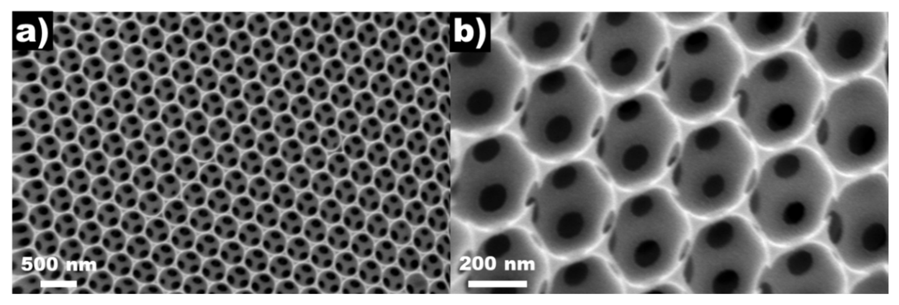
2.1. Geometrical Features

The PCs are formed using an established polystyrene (PS) templating methodology [26], where the ordered polystyrene (PS) film is initially deposited onto a vertically aligned FTO glass substrate as a soft template via evaporation of a PS emulsion. The FTO precursor (please see Section 3.3) is then infiltrated and calcinated to give PC FTO electrode. It should be noted that the pore size of PCs is commonly smaller than that of polymer spheres due to the shrinkage during heat-treatment. As shown by scanning electron microscopy (SEM), the as-prepared PC FTO film was highly ordered with periodic FTO walls and spherical air pores ca. 300 nm in diameter (Figure 1a), and the interconnected voids on FTO walls allow the diffusion of electrolyte (Figure 1b) among the pores. The close-packed air spheres from the top view correspond to the (111) plane in a typical fcc structure; this predominant plane is mainly responsible for the PSB generation [27]. Using PS spheres of different diameters as templates would not only vary the pore size and surface area of PC FTO film, but also change the PSB range. (Please see supporting information for details).

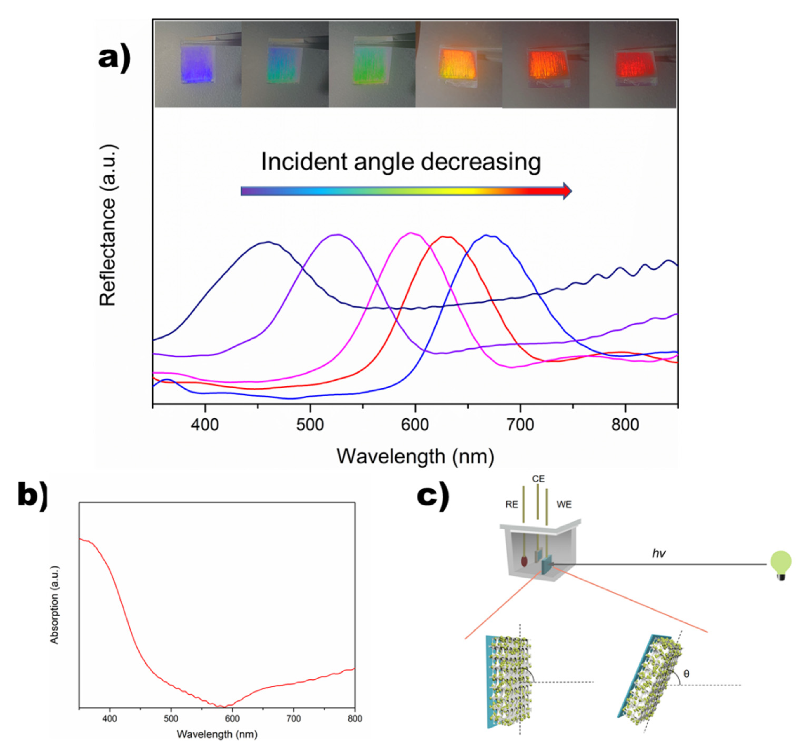
2.2. Optical Features

The diffuse-reflectance spectra (DRS) of PC FTO is illustrated below, in which the PSB is recorded from one PC FTO photoelectrode under different incidence relative to its surface normal. The PSB position of PC FTO with pore size ca. 300 nm can be shifted in almost the whole visible range (Figure 2a). The CdS nanoparticles synthesized on PC FTO substrate presents the absorption at ca. 475 nm (Figure 2b), which can be compared to the bulk CdS (ca. 510 nm, Figure S5) synthesized using the same method The reduced size of CdS can be attributed to the PCs acting as seeds and allowing less aggregation of ions from precursor solution, in comparison to that in pure solution systems. This phenomenon was also observed in several other systems [28].
This PSB shift can also be identified by eye when being illuminated (the inserts (photographs) at the top of Figure 2a), in which the photoelectrode exhibits color from violet to red. The intensive PSB and shining color can represent the homogeneity and highly ordered array of the PC FTO film. The coverage of PSB in scale of wavelength from different PC FTO photoelectrodes under incidence (relative to surface normal) is shown in Table S1, which was concluded from the Bragg–Snell equation below [29,30,31]. D is the periodic order (the shortest distance between the centers of two air pore; h, k and l are the planes in order; ϕ is the filling factor (0.26 for a fcc close-packed structure); n and n0 are the refractive index of FTO (1.61) and air (1.00) accordingly; and θ is the light incident angle. It should be noted that the PSB may not be generated from only (111) plane; the planes with all even or all odd h,k,l indices (e.g., (220), (222), (133)) would also possibly contribute extra PSB [27].
PSB = d h k l m [ φ n 2 + ( 1 φ ) n 0 2 s i n 2 θ ] 1 2
d h k l = D 2 [ h 2 + k 2 + l 2 ] 1 2

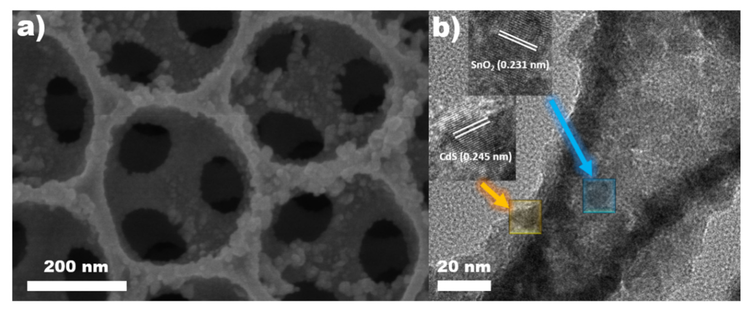
2.3. Loading the PC FTO Photoelectrode with CdS Nanoparticles

As shown in Figure 3a, the detailed morphology of the as-prepared CdS/PC FTO photoelectrode is presented by transmission electron microscopy (TEM). The CdS nanoparticles are ca. 5–10 nm each and homogeneously loaded onto the walls of PC FTO. It should be noted that the doped fluorine in FTO is typically below 0.5 atom % [32], so that the FTO exhibits crystal structure very close to SnO2 [33]. High-resolution transmission electron microscopy (HR-TEM) confirmed the lattice fringes from SnO2 and CdS, corresponding to (111) and (102) planes, respectively (Figure 3b). Powder X-ray diffraction (PXRD, Figure S1) shows peaks consistent with the results from HR-TEM, which can be indexed to JCPDS 64-3414 (CdS) and 41-1445 (SnO2). In addition, the elemental distribution is presented in Figure S2; we used TEM-energy dispersive X-ray spectroscopy (TEM-EDX) to further identify the composition of as-prepared CdS/PC FTO photoelectrode. As a result, the successful loading allows the CdS nanoparticles to benefit from the photonic effects and high surface area supplied by PC FTO photoelectrode.

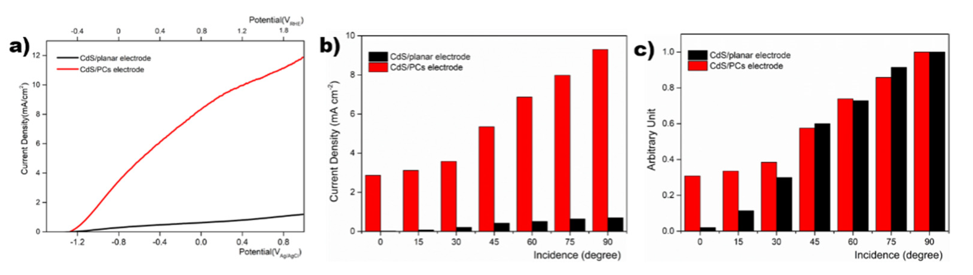
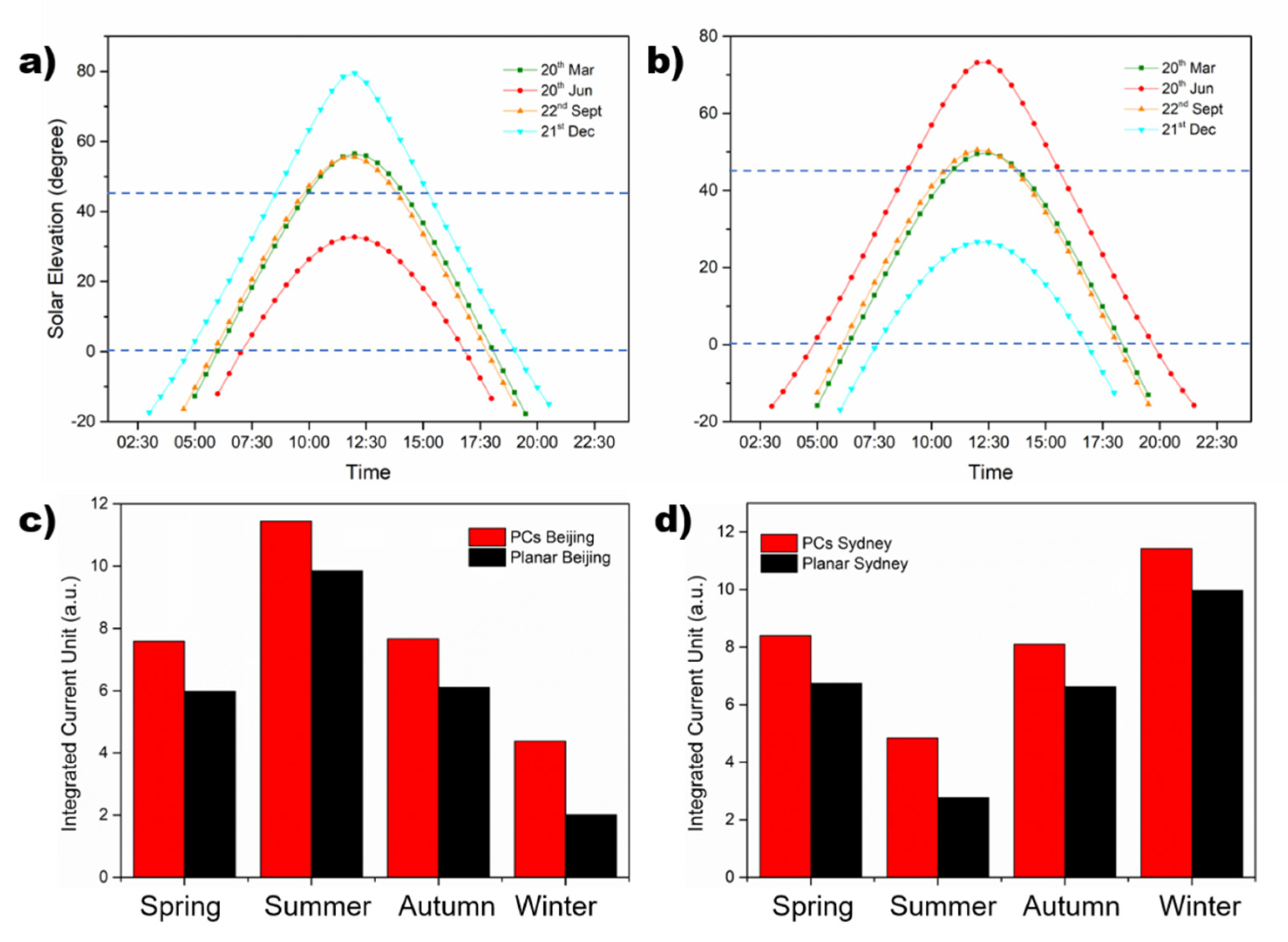
2.4. Integrated PEC Photocurrent Generation from the PC FTO Photoelectrode

As a conductive material, PC FTO have been commonly used as suppliers of high surface area and photonic effect in the PEC cell [34,35]. The more efficient utilizations of solar energy for PCs based photoelectrode could be attributed to two reasons: (1) Increased surface area available for loading more photoactive materials. (2) Multiple scattering and refraction, which would dramatically enhance the possibility of photon harvesting for the loaded photoactive materials, especially under lower incident angles. In order to evaluate the influences of photonic effects on the PEC performance, the CdS was loaded on a planar FTO photoelectrode as a control group. The working area of the planar FTO electrode was designed to be 1 cm2. On the other hand, the working area of the PC FTO was confirmed through an electrochemical Faradaic capacitance [36] measurement (Figure S3), giving a surface area of ca. 16 cm2. The reason for not applying the most common BET method to estimate the surface area of PC FTO is due to the low mass (in micro gram scale) of the PC FTO film.
The setup of PEC cell is illustrated in Figure 2c, based on a standard three-electrode system. The sample, Pt sheet and Ag/AgCl were exploited as the working electrode, counter electrode and reference electrode, respectively. Linear sweep voltammetry (LSV) was carried out from −1.2 to 1.0 V vs. VAg/AgCl in Na2SO3(aq.)/Na2S(aq.) (0.35 M/0.25 M) electrolyte; both the photoelectrodes presented the onset potential at ca. −1.2 V and the current density was ca. 9.3 and 0.7 mA cm−2 at 0 V vs. VAg/AgCl for a PC electrode and planar electrode, respectively. The variation of incident angles from the simulated solar light (relative to the surface normal of photoelectrode) was obtained by rotating the working electrode to certain angles. The photocurrent density of the photoelectrode from certain incidence was recorded via the i-t curves at a bias of 0 V vs. VAg/AgCl (Figure S4). In terms of the CdS/planar-FTO, the photocurrent density was steadily reduced along with the decreasing incidence (Figure 4b,c). The photocurrent density decreased over 97% under incident illumination from 90° to 0°; this trend is consistent with previous literature [37]. On the other hand, the photocurrent density of CdS/PC FTO photoelectrode presents a similar reducing trend comparing with that of planar FTO from 90° to 45°, and only lost 8% current density from 45 ° to 0 °, which is much less than that of the planar electrode (28 %, Figure 4c), and this result can also be compared to C3N4/PC FTO (16 %) [13]. These results suggest that the PC electrode can significantly improve the light harvesting under a certain angle (below 45°) of incidence.
To estimate the practical performances of the PC FTO photoelectrode, the solar elevations of two typical cities from sunrise to sunset in four seasons are listed in Figure 5a,b. The approximate duration of solar elevation in range 0° to 45° that accounts for the sunshine time is 69.3 % (spring), 55.7 % (summer), 72.9 % (autumn) or 100 % (winter) in Beijing, and 64.5 % (spring), 100 % (summer), 64.5 % (autumn) or 52.5 % (winter) in Sydney. This suggests the significance of the PC photoelectrode due to the improved utilization of light with this incident range. According to the above-mentioned solar elevation data, the simulated photocurrent densities generated in a day from these two cities in certain seasons are exhibited in Figure 5c,d, where incidence is applied as the only variable quantity. The current density of a PC electrode is ca. 2-fold that of a planar electrode in winter in Beijing and in summer in Sydney, and ca. 20% greater than that in other three seasons. These improvements can be concluded as the promising light scattering properties of the PCs, which could remarkably enhance the light harvesting when under lower incidence.

3. Experimental

3.1. General

Ethanol (99.99%), H2SO4 (≥95%), H2O2 (30%), FTO coated glass slides (7 Ω/sq), SnCl4·5H2O (99.99%), NH4F (99.99%), Na2S·9H2O, Na2SO3, Cd(Ac)2·2H2O and KCl were purchased from Sigma Aldrich and used as received.
SEM images were obtained using an FEI Sirion scanning electron microscope (Hilboro, OR, USA) operating at 5–10 kV. Prior to imaging, samples were supported on an aluminum stub with an adhesive carbon tab and sputter coated with a 10 nm layer of carbon using an Agar auto carbon coater. Energy dispersive analysis of X-rays (EDAX) was performed using an attached EDAX Phoenix X-ray spectrometer (Phoenix, EDAX, Mahwah, NJ, USA). TEM images were obtained using a JEOL 2011 transmission electron microscope (Tokyo, Japan) operated at 200 kV accelerating voltage. TEM samples were ground and sonicated in methanol, and a drop of the dispersion evaporated onto a holey carbon, copper grid. Transmission and UV–Vis spectra were recorded on an Ocean Optics HR2000+ High Resolution Spectrometer (Largo, FL, USA) with a DH-2000-BAL Deuterium/Helium light source (200–1100 nm). A R400-7-UV-Vis reflection probe (Largo, FL, USA) was used to record diffuse reflectance spectra. Spectra were recorded in Spectra Suite software using an integration time of 10 s, box car smoothing width of 30 and 10 scans to average. PXRD patterns were recorded on a Bruker-AXS D8 Advance (Karlsruhe, Germany) instrument with Lynx eye detector, using Cu Kα radiation, scanning in the range 5–70 (2θ), with a 0.02° step size and each data point collected for 0.05 s.
Electrochemical measurements were made using a standard 3-electrode configuration. The reference electrode was Ag/AgCl (3 M NaCl internal solution), and a platinum wire was used as the counter electrode. Connection to the FTO working electrode was achieved using copper tape, and the bottom 10 mm of the electrode was immersed in the electrolyte solution to give a working area of 1 cm2. The photoelectrochemical cell contained a Pyrex window through which the electrode was back-illuminated using a filtered (>400 nm) 150 W Xe lamp with an irradiance of 100 mWcm−2. Electrolyte solutions were prepared using water filtered using a Millipore system (>18 MΩ cm−3), and degassed for 10 min with N2 before use. PC FTO electrodes without CdS were measured in an electrolyte of KCl(aq) solution (0.1 M, pH 7) and electrodes coated with CdS were measured in an electrolyte of aqueous Na2S(aq)/Na2SO3(aq) (0.25/0.35 M) (pH 13). All potentials are referenced to the reversible hydrogen electrode using the following equation.
E RHE = E vsAg / AgCl + E ref ( Ag / AgCl ) + 0.059 pH
where Eref (Ag/AgCl) = 0.209 V vs. NHE at 25 °C.

3.2. Polystyrene (PS) Template Film Formation

Planar FTO coated electrodes (2 × 10 × 15 mm) were soaked in piranha solution (3:1 H2SO4:H2O2) for 2 h, washed with deionized water and dried under a stream of N2. An electrode was stood vertically in a glass vial containing a suspension of PS spheres dispersed in ethanol and water (1:82:8 PS:ethanol:water) to a level just above the top of the electrode. The volatiles were evaporated over ca. 15 h at 60 °C until 10 mm of film was deposited. The electrode was then removed and the remaining 5 mm cleaned with acetone, giving an electrode coated with a continuous opalescent polystyrene film 10 × 10 mm and ca. 7–10 μm thick.

3.3. Photonic Crystal FTO (PC FTO) Electrode

FTO precursor solution was prepared from SnCl4·5H2O (1.4 g, 4.01 mmol)) sonicated in ethanol (20 mL) until dissolved, and then saturated (ca 45 g in 100 mL) NH4F solution (0.24 g, 2.01 mmol) was added, and the resulting mixture sonicated until optically clear and colorless. A PS template coated electrode was pre-soaked in ethanol for 30 min before being stood vertically and submerged in the FTO precursor solution (3.5 mL) in a glass vial and stored in a desiccator under a partial vacuum for 30 min. The electrode was removed from the vial and FTO precursor solution (20 μL) was dropped onto the wet film which was then calcined in air at 450 °C for 2 h using a heating ramp rate of 1 °C min−1.

3.4. Coating of the PC FTO with a Continuous CdS Film

In a glass vial a PC FTO electrode was stood vertically in a solution of Cd(Ac)2 in ethanol (50 mM) for 1 min, removed and then dried under a stream of N2. The electrode was then stood vertically in a second glass vial containing an aqueous solution of N2S (50 mM) for 1 min, rinsed with distilled water and dried under a stream of N2. This cycle was repeated from 1 to 10 times. The electrode was finally heated under argon at 400 °C for 30 min using a ramp-up rate of 1 °C min−1.

4. Conclusions

In summary, CdS nanoparticles as a photoactive material were in-situ loaded in PC FTO and planar FTO to investigate the incidence-dependent PEC performance. The PC FTO exhibited promising light scattering effects, especially when the incidence was lower than 45°, thereby enhancing the photocurrent generation under practical conditions. The simulated photocurrent generation from the photoelectrode in two example cities was also carried out to estimate the realistic value of the PC electrode.

Supplementary Materials

The following are available online at https://www.mdpi.com/2073-4344/10/11/1252/s1, Figure S1: (a) PXRD of the aluminum holder used for the test, (b) as-prepared PCs FTO loaded with CdS nanoparticles; Table S1: The PSB as a function of PS size and incidence under standard conditions; Figure S2: TEM-EDX elemental mapping of the as-prepared PCs FTO loaded with CdS nanoparticles; Figure S3: Capacitance measurements of (a) planar FTO and (b) PCs FTO via cyclic voltammetry. Capacitance is derived from the gradient of current vs. scan rate for (c) planar FTO substrate 0V vs. Ag/AgCl and (d) PCs FTO at 0.06V vs. Ag/AgCl; Figure S4: i-t curves of CdS/PCs FTO photoelectrode under different incident illumination, the light source is chopped for every 10 seconds. Conditions: 100 mW cm−2 Xe lamp, 0 V vs. VAg/AgCl, in Na2SO3(aq.)/Na2S(aq.) (0.35 M/0.25 M); Figure S5: (a) SEM image and (b) absorption spectra of bulk CdS synthesized using SILAR method in absence of substrate.

Author Contributions

Conceptualization, M.Z. and K.W.; methodology, X.K.; software, W.W.; validation, M.Z., X.K. and K.W.; formal analysis, M.Z.; investigation, C.T.; resources, K.W.; data curation, X.K.; writing—original draft preparation, K.W.; writing—review and editing, M.Z.; visualization, supervision, M.Z.; project administration, M.Z.; funding acquisition, D.L. All authors have read and agreed to the published version of the manuscript.

Funding

The authors acknowledge funding from the Guangdong Basic and Applied Basic Research Foundation (grant number 2020B1515020032), the Pearl River S&T Nova Program of Guangzhou (grant number 201906010058), the Science and Technology Program of Guangzhou (grant number 2019050001), the Guangdong Science and Technology Plan (grant number 2019B040403003) and the National Natural Science Foundation of China (grant number 61704034).

Conflicts of Interest

The authors declare no conflict of interest.

References

  1. Archer, M.D.; Nozik, A.J. Nanostructured and Photoelectrochemical Systems for Solar Photon Conversion; Imperial College Press: London, UK, 2008; Volume 3. [Google Scholar]
  2. Jiang, C.; Moniz, S.J.A.; Wang, A.; Zhang, T.; Tang, J. Photoelectrochemical devices for solar water splitting–materials and challenges. Chem. Soc. Rev. 2017, 46, 4645–4660. [Google Scholar] [CrossRef] [Green Version]
  3. Walter, M.G.; Warren, E.L.; McKone, J.R.; Boettcher, S.W.; Mi, Q.; Santori, E.A.; Lewis, N.S. Solar Water Splitting Cells. Chem. Rev. 2010, 110, 6446–6473. [Google Scholar] [CrossRef] [PubMed]
  4. Khan, Q.; Subramanian, A.; Yu, G.; Maaz, K.; Li, D.; Sagar, R.U.R.; Chen, K.; Lei, W.; Shabbir, B.; Zhang, Y. Structure optimization of perovskite quantum dot light-emitting diodes. Nanoscale 2019, 11, 5021–5029. [Google Scholar] [CrossRef]
  5. Yin, X.L.; Li, L.L.; Jiang, W.J.; Zhang, Y.; Zhang, X.; Wan, L.J.; Hu, J.S. MoS2/CdS Nanosheets-on-Nanorod Heterostructure for Highly Efficient Photocatalytic H2 Generation under Visible Light Irradiation. ACS Appl. Mater. Interfaces 2016, 8, 15258–15266. [Google Scholar] [CrossRef]
  6. Wang, Y.; Zhen, W.; Zeng, Y.; Wan, S.; Guo, H.; Zhang, S.; Zhong, Q. In situ self-assembly of zirconium metal–organic frameworks onto ultrathin carbon nitride for enhanced visible light-driven conversion of CO2 to CO. J. Mater. Chem. A 2020, 8, 6034–6040. [Google Scholar] [CrossRef]
  7. Li, Y.; Fu, Z.-Y.; Su, B.-L. Hierarchically Structured Porous Materials for Energy Conversion and Storage. Adv. Funct. Mater. 2012, 22, 4634–4667. [Google Scholar] [CrossRef]
  8. Collins, G.; Armstrong, E.; McNulty, D.; O’Hanlon, S.; Geaney, H.; O’Dwyer, C. 2D and 3D photonic crystal materials for photocatalysis and electrochemical energy storage and conversion. Sci. Technol. Adv. Mater. 2016, 17, 563–582. [Google Scholar] [CrossRef] [Green Version]
  9. Zheng, X.; Zhang, L. Photonic nanostructures for solar energy conversion. Energy Environ. Sci. 2016, 9, 2511–2532. [Google Scholar] [CrossRef]
  10. Ming, J.; Liu, A.; Zhao, J.; Zhang, P.; Huang, H.; Lin, H.; Xu, Z.; Zhang, X.; Wang, X.; Hofkens, J.; et al. Hot pi-Electron Tunneling of Metal-Insulator-COF Nanostructures for Efficient Hydrogen Production. Angew. Chem. 2019, 58, 18290–18294. [Google Scholar] [CrossRef]
  11. Pi, M.; Wang, X.; Zhang, D.; Wang, S.; Chen, S. A 3D porous WP2 nanosheets@carbon cloth flexible electrode for efficient electrocatalytic hydrogen evolution. Front. Chem. Sci. Eng. 2018, 12, 425–432. [Google Scholar] [CrossRef]
  12. Xiang, L.; Zhao, X. Wet-Chemical Preparation of TiO2-Based Composites with Different Morphologies and Photocatalytic Properties. Nanomaterials 2017, 7, 310. [Google Scholar] [CrossRef] [PubMed] [Green Version]
  13. Xiao, Y.; Chen, M.; Zhang, M. Improved Utilization of Sunlight Through the Incidence Dependence of the Photonic Stop Band: A g-C3N4-Embedded Fluorine-Doped Tin Oxide (FTO) Photonic Crystal Film. ChemPhotoChem 2019, 3, 101–106. [Google Scholar] [CrossRef]
  14. Ellmer, K. Past achievements and future challenges in the development of optically transparent electrodes. Nat. Photon. 2012, 6, 809–817. [Google Scholar] [CrossRef]
  15. Nishimoto, N.; Yamada, Y.; Ohnishi, Y.; Imawaka, N.; Yoshino, K. Effect of temperature on the electrical properties of ITO in a TiO2 /ITO film. Phys. Status Solidi (a) 2013, 210, 589–593. [Google Scholar] [CrossRef]
  16. Yang, Z.; Gao, S.; Li, T.; Liu, F.-Q.; Ren, Y.; Xu, T. Enhanced Electron Extraction from Template-Free 3D Nanoparticulate Transparent Conducting Oxide (TCO) Electrodes for Dye-Sensitized Solar Cells. ACS Appl. Mater. Interfaces 2012, 4, 4419–4427. [Google Scholar] [CrossRef]
  17. Yuan, S.; Huang, H.; Wang, Z.; Zhao, Y.; Shi, L.; Cai, C.; Li, D.D. Improved electron-collection performance of dye sensitized solar cell based on three-dimensional conductive grid. J. Photochem. Photobiol. A Chem. 2013, 259, 10–16. [Google Scholar] [CrossRef]
  18. Ahmad, M.S.; Pandey, A.; Rahim, N.A. Advancements in the development of TiO2 photoanodes and its fabrication methods for dye sensitized solar cell (DSSC) applications. A review. Renew. Sustain. Energy Rev. 2017, 77, 89–108. [Google Scholar] [CrossRef]
  19. Tang, M.H.; Chakthranont, P.; Jaramillo, T.F. Top-down fabrication of fluorine-doped tin oxide nanopillar substrates for solar water splitting. RSC Adv. 2017, 7, 28350–28357. [Google Scholar] [CrossRef] [Green Version]
  20. Xie, Z.; Zhang, Q.; Liu, Q.; Zhai, J.; Diao, X. Enhanced electrochromic performance of 2D grid-structured WO3 thin films. Thin Solid Films 2018, 653, 188–193. [Google Scholar] [CrossRef]
  21. Li, J.; Qiu, Y.; Wei, Z.; Lin, Q.; Zhang, Q.; Yan, K.; Chen, H.; Xiao, S.; Fan, Z.; Yang, S. A three-dimensional hexagonal fluorine-doped tin oxide nanocone array: A superior light harvesting electrode for high performance photoelectrochemical water splitting. Energy Environ. Sci. 2014, 7, 3651–3658. [Google Scholar] [CrossRef]
  22. Xie, J.; Yang, P.; Liang, X.; Xiong, J. Self-Improvement of Ti:Fe2O3 Photoanodes: Photoelectrocatalysis Improvement after Long-Term Stability Testing in Alkaline Electrolyte. ACS Appl. Energy Mater. 2018, 1, 2769–2775. [Google Scholar] [CrossRef]
  23. Yang, Z.; Gao, S.; Li, W.; Vlasko-Vlasov, V.; Welp, U.; Kwok, W.-K.; Xu, T. Three-Dimensional Photonic Crystal Fluorinated Tin Oxide (FTO) Electrodes: Synthesis and Opstical and Electrical Properties. ACS Appl. Mater. Interfaces 2011, 3, 1101–1108. [Google Scholar] [CrossRef]
  24. Gun, Y.; Song, G.Y.; Quy, V.H.V.; Heo, J.; Lee, H.; Ahn, K.-S.; Kang, S.-H. Joint Effects of Photoactive TiO2 and Fluoride-Doping on SnO2 Inverse Opal Nanoarchitecture for Solar Water Splitting. ACS Appl. Mater. Interfaces 2015, 7, 20292–20303. [Google Scholar] [CrossRef]
  25. Cho, S.Y.; Kang, S.H.; Yun, G.; Balamurugan, M.; Ahn, K.S. Annealing Effect of Fluorine-Doped SnO2/WO3 Core-Shell Inverse Opal Nanoarchitecture for Photoelectrochemical Water Splitting. J. Korean Phys. Soc. 2017, 70, 162–168. [Google Scholar] [CrossRef]
  26. Luo, D.; Chen, Q.; Qiu, Y.; Liu, B.; Zhang, M. Carbon Dots-Decorated Bi2WO6 in an Inverse Opal Film as a Photoanode for Photoelectrochemical Solar Energy Conversion under Visible-Light Irradiation. Materials 2019, 12, 1713. [Google Scholar] [CrossRef] [PubMed] [Green Version]
  27. Stein, A.; Wilson, B.E.; Rudisill, S.G. Design and functionality of colloidal-crystal-templated materials—chemical applications of inverse opals. Chem. Soc. Rev. 2013, 42, 2763–2803. [Google Scholar] [CrossRef]
  28. Kanai, T.; Sano, K.; Yano, H.; Sawada, T. Independent control of optical stop-band wavelength and width of colloidal photonic crystals. Colloids Surfaces A Physicochem. Eng. Asp. 2016, 506, 586–590. [Google Scholar] [CrossRef]
  29. Hu, J.; Yang, M.; Ke, X.; Yang, S.; Wang, K.; Huang, H.; Wang, W.; Luo, D.; Zheng, Z.; Huang, L.; et al. Cubic-cubic perovskite quantum dots/PbS mixed dimensional materials for highly efficient CO2 reduction. J. Power Sources 2021, 481, 228838. [Google Scholar] [CrossRef]
  30. Huang, H.; Yuan, H.; Zhao, J.; Solís-Fernández, G.; Zhou, C.; Seo, J.W.; Hendrix, J.; Debroye, E.; Steele, J.A.; Hofkens, J.; et al. C(sp3)–H Bond Activation by Perovskite Solar Photocatalyst Cell. ACS Energy Lett. 2018, 4, 203–208. [Google Scholar] [CrossRef] [Green Version]
  31. Huang, H.; Yuan, H.; Janssen, K.P.F.; Solís-Fernández, G.; Wang, Y.; Tan, C.Y.X.; Jonckheere, D.; Debroye, E.; Long, J.; Hendrix, J.; et al. Efficient and Selective Photocatalytic Oxidation of Benzylic Alcohols with Hybrid Organic–Inorganic Perovskite Materials. ACS Energy Lett. 2018, 3, 755–759. [Google Scholar] [CrossRef] [Green Version]
  32. Liu, H.; Sun, H.; Liu, L.; Hou, X.; Jia, X. Optical properties of porous anodic alumina embedded Cu nanocomposite films. Opt. Mater. 2015, 44, 9–12. [Google Scholar] [CrossRef]
  33. Keller, D.A.; Barad, H.-N.; Rosh-Hodesh, E.; Zaban, A.; Cahen, D. Can fluorine-doped tin Oxide, FTO, be more like indium-doped tin oxide, ITO? Reducing FTO surface roughness by introducing additional SnO2 coating. MRS Commun. 2018, 8, 1358–1362. [Google Scholar] [CrossRef]
  34. Banyamin, Z.Y.; Kelly, P.J.; West, G.; Boardman, J. Electrical and Optical Properties of Fluorine Doped Tin Oxide Thin Films Prepared by Magnetron Sputtering. Coatings 2014, 4, 732–746. [Google Scholar] [CrossRef]
  35. Cui, X.; Wang, Y.; Jiang, G.; Zhao, Z.; Xu, C.; Wei, Y.; Duan, A.; Liu, J.; Gao, J. A photonic crystal-based CdS–Au–WO3 heterostructure for efficient visible-light photocatalytic hydrogen and oxygen evolution. RSC Adv. 2014, 4, 15689–15694. [Google Scholar] [CrossRef]
  36. Wang, Z.; Li, X.; Ling, H.; Tan, C.K.; Yeo, L.P.; Grimsdale, A.C.; Tok, A. 3D FTO/FTO-Nanocrystal/TiO2 Composite Inverse Opal Photoanode for Efficient Photoelectrochemical Water Splitting. Small 2018, 14, 1800395. [Google Scholar] [CrossRef]
  37. Wu, X.; Zhou, J.; Xing, W.; Zhang, Y.; Bai, P.; Xu, B.; Zhuo, S.; Xue, Q.; Yan, Z. Insight into high areal capacitances of low apparent surface area carbons derived from nitrogen-rich polymers. Carbon 2015, 94, 560–567. [Google Scholar] [CrossRef]
Figure 1. SEM images of the as-prepared PC FTO photoelectrode at (a) low magnification and (b) high magnification.
Catalysts 10 01252 g001
Figure 2. (a) DRS and digital photographs of a PC FTO (pore size of ca. 300 nm) photoelectrode under different incident angle illumination; the PSB is expressed as the reflectance peaks; (b) the absorption spectra of CdS nanoparticles; (c) the setup of CdS-loaded PC FTO photoelectrode in the PEC cell.
Catalysts 10 01252 g002
Figure 3. (a) TEM image of CdS/PC FTO and (b) HR-TEM of CdS/PC FTO; the lattice fringes correspond to JCPDS numbers of 64-3414 (CdS) and 41-1445 (SnO2), respectively.
Catalysts 10 01252 g003
Figure 4. (a) LSV curves of CdS-loaded CdS/PC FTO and CdS/planar FTO photoelectrode; (b) current density of CdS/PC FTO and CdS/planar FTO photoelectrode under incidence from 90° to 0°; (c) the relative current density in comparison to that under 90° illumination.
Catalysts 10 01252 g004
Figure 5. The solar elevations of (a) Sydney and (b) Beijing in the four seasons. The data were collected from NOAA Earth System Research Laboratories (ESRL); the overall photocurrent density generated in a day in (c) Beijing and (d) that generated in Sydney; the current density was normalized to get rid of the influence from the large surface area supplied by PC FTO.
Catalysts 10 01252 g005
Publisher’s Note: MDPI stays neutral with regard to jurisdictional claims in published maps and institutional affiliations.

