1. Introduction
Current research trends focus on developing thin film materials, especially semi-conducting oxides, due to their wide number of technological applications such as in the field of optics, sensors, microelectronics, electrocatalysis, and energy production [
1,
2,
3,
4]. In addition, the rapid growth of industrial demand on reducing the materials’ cost leads to downscaling the amount of materials in terms of film thickness. Moreover, the application of these conformal thin film materials to catalytic systems has begun to attract much attention, and the capacity to deposit these thin catalytic films in a highly controlled manner continues to gain importance [
5]. Atomic layer deposition (ALD), a special type of chemical vapor deposition (CVD) technique, is considered as one of the most attractive thin film deposition techniques where the conformality, uniformity, and thickness controllability of the films are crucial [
6]. This technique relies on the successive, separated, and self-terminating gas–solid reactions of typical two gaseous reactants [
7]. During the past decades, hundreds of materials have been explored and have been developed using this technique, and it has successfully demonstrated its importance in the thin film electroluminescent display production. However, the industrial use of this technique remained marginal for more than two decades [
8].
In the industry, roll-to-roll and continuous ALD coating technology has been developed where the typical process conditions applied are 0.1 to 10 mbar or atmospheric pressure and a temperature range of 50 to 500 °C. Additionally, ALD is not limited to film deposition but can also be applied on particles and powders. Currently, the ALD process can be used to deposit a wide range of binary oxides, nitrides, carbides, metals, sulfides, fluorides, polymers, and mixed structures [
9].
Looking at the side of energy production, hydrogen is one of the promising sustainable solutions for the energy problem. One of the most efficient ways of producing H
2 at low cost and high purity is the electrochemical water splitting into hydrogen and oxygen. However, this process is still not optimal because of the sluggish kinetics of the anodic oxygen evolution reaction (OER) subsequently due to the well-known scaling relation restriction [
10]. This eventually leads to the increase in the operating cell voltage for the electrolysis and to the challenges faced for the large-scale commercialization of the technology. A number of metal oxides have been tested as electrocatalysts, and nickel and noble metal oxides have shown suitable qualities as anode materials both in acidic and alkaline media [
11]. Numerous studies [
11,
12,
13] have already discussed the use of transition metal oxides as the most suitable OER electrode material. Furthermore, industries have strict requirements for an electrode material such as high surface area, high electrical conductivity, good weldability, good electrochemical activity (measured through the oxygen overpotential values) and stability over several years, low cost, and safe in terms of the environment, health, and safety (EHS).
In this work, iridium dioxide (IrO2) and nickel oxide (NiO) thin films were deposited on Ni expanded mesh suitable for industrial applications and on an Si (100) substrate, which served as a reference material. Then, thin films deposited on Ni-expanded meshes were applied as anodes for alkaline water electrolysis. The choice of these two materials comes from the need to demonstrate the electrochemical activity of thin films for what are known to be particularly active noble and non-noble metal oxides for oxygen evolution reaction. ALD operating parameters such as the total number of deposition cycles, deposition and sublimation temperatures, precursors pulse, and purge lengths were varied to determine their effect on the structure and electrochemical performance of the synthesized (thin film) material. The electrochemical tests done in this study are pushing the boundaries of the single electrode potential at the highest values of current densities so far reported in the literature. In addition, these tests were done to demonstrate the functionality of the anodes suitable to the industrial needs for the deployment of the next generation of alkaline water electrolysis for the stationary energy storage application. The samples were characterized using various structural and morphological characterization techniques: XRR (X-ray reflectivity), GIXRD (grazing-incidence X-ray diffraction), XRF (X-ray fluorescence), and SEM (scanning electron microscopy). The electrochemical activity, in terms of oxygen overpotential value, was measured using iR-SEP (iR-corrected single electrode potential) tests, where resistance measurements were done using EIS (electrochemical impedance spectroscopy).
2. Results
In the proceeding sections, synthesized thin film metal oxides are referred to as Samples A to D (for NiO samples) and Samples E to H (for IrO
2 samples). The number that follows the letter refers to the pre-treatment method performed on the Ni expanded mesh substrates: 1—for sandblasted and acid etched; and 2—for not sandblasted but acid etched; otherwise stated, the substrate used is Si (100). All the Ni expanded meshes are proprietary of Industrie De Nora S.p.A. (Milan, Italy). For other details of the substrate pre-treatment, see
Section 4.
2.1. Film Thickness and Catalyst Loading
The thickness of the films was measured, and the total catalyst loading was estimated by the change in the mass of the samples before and after the deposition. The film thickness of NiO was measured using XRR on the samples deposited on the Si (100) substrate. Moreover, for the more accurate film thickness of IrO2 samples, EDX results analyzed using a GMR electron probe thin film microanalysis program was used. This is also done to integrate various characterization techniques.
As discussed by Miikkulainen V. et al. [
7], one deposition cycle consists typically of four steps: (1) Step 1a: gas–solid reaction (chemisorption reaction) of the first reactant (Reactant A), typically of a metal reactant; (2) Step 1b: purge or evacuation to remove the unreacted precursor and gaseous by-products; (3) Step 2a: second gas–solid reaction (chemisorption reaction) of the second reactant (Reactant B), typically of a non-metal reactant; and (4) Step 2b: purge or evacuation to remove the unreacted precursor and gaseous by-products.
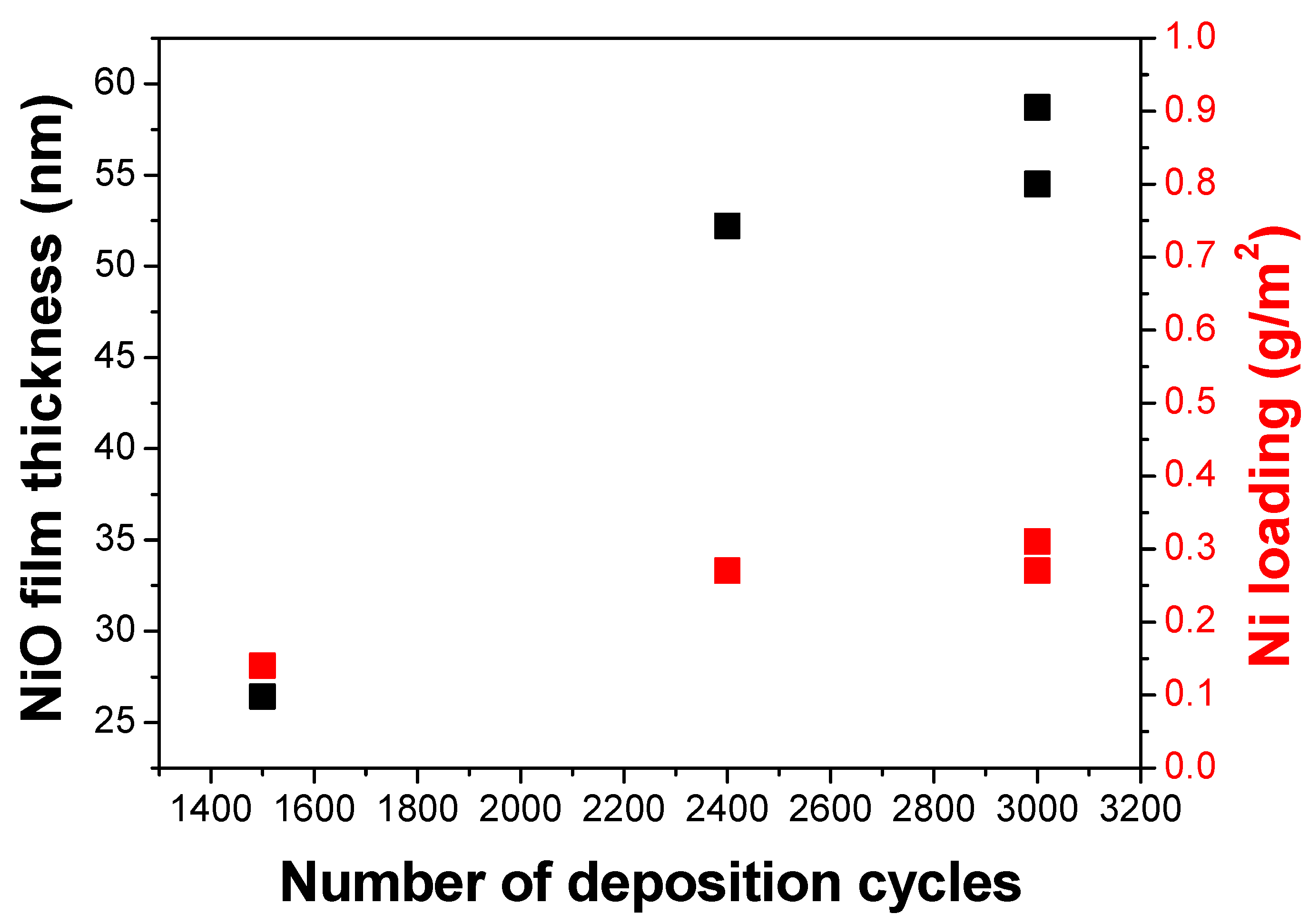
Table 1 shows the calculated film thickness and metal loading of the samples at a different total number of deposition cycles (sum of cycles for the ‘front’ and ‘back’ side of the electrode). The ‘front’ side of the electrode is the side facing the top, while the ‘back’ is facing the bottom during the first half of the deposition cycle. For the second half of the deposition cycle, the electrode was turned over, making the ‘front’ side facing the bottom. NiO samples have approximately 26 to 59 nm thickness, while IrO
2 samples have 49 to 59 nm film thickness.
It can be noted that for the IrO
2 samples, only one deposition cycle set (2000 cycles) was performed in this work, which was based on the previously reported study [
6]. However, for the NiO samples, a different total number of deposition cycles was studied, and
Figure 1 shows the linear relation of the total number of deposition cycles on the film thickness and metal loading, as also observed by Hämäläinen J. et al. [
6].
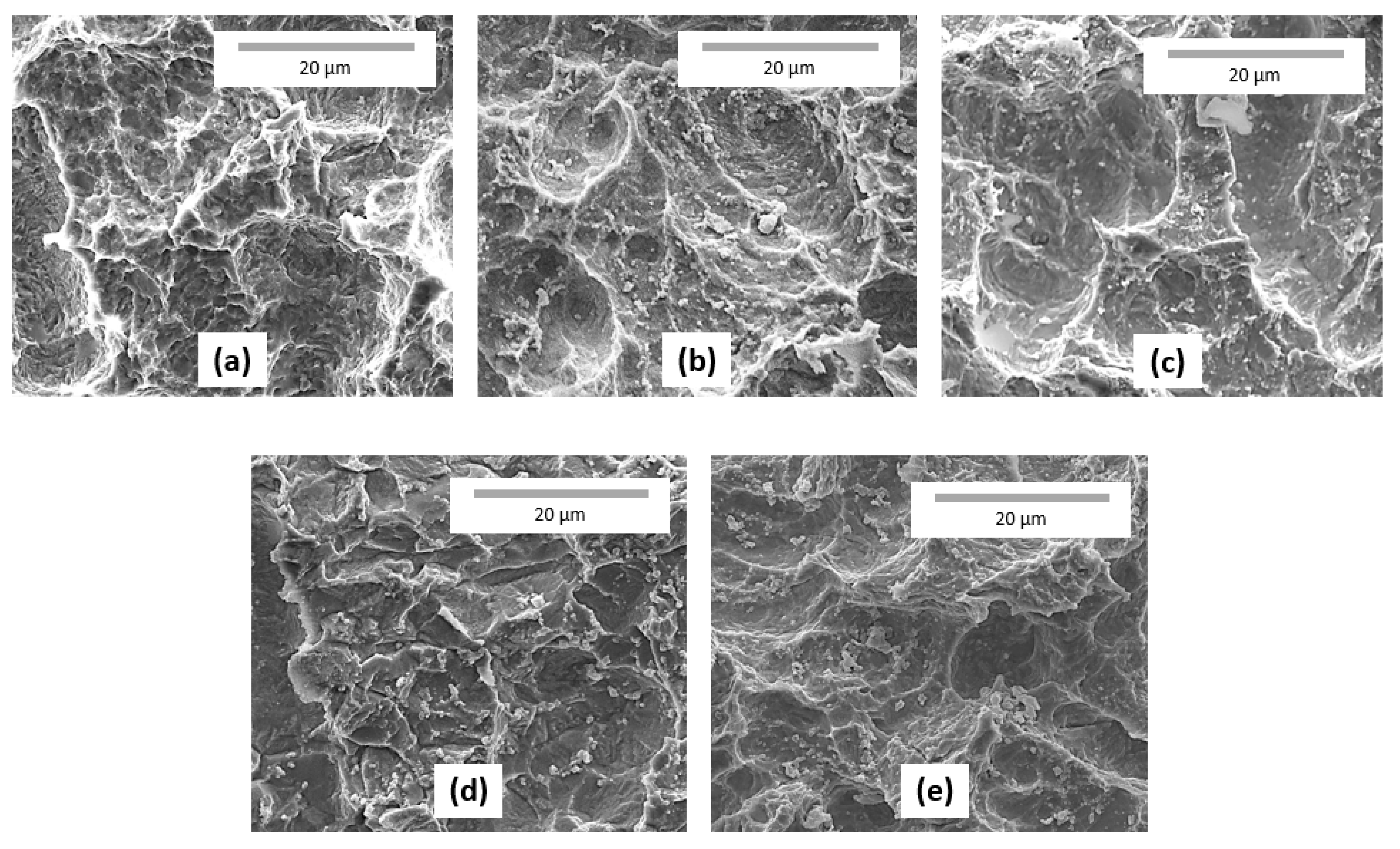
As mentioned earlier, one feature of the ALD technique is the uniformity of the films deposited. To verify this, SEM images on the IrO
2 thin films on the sandblasted substrate are shown in
Figure 2. It can be observed from these images that the deposited thin films appear to be uniformed over the whole surface irrespective of the substrate surface roughness or defects. This uniformed deposition offers more advantage than other deposition methods (i.e., evaporation) that usually leads to reduced coating thickness on the edges or other parts of the substrate and sometimes no coating at all.
Figure 3 shows the XRF results (in terms of iridium counts) on the IrO
2 samples. This analysis was not possible for the NiO samples due to the limitation of the technique regarding distinguishing the Ni content from the coating itself and from the substrate. XRF analysis in this case was done as a rapid screening (semi-quantitative analysis) to determine if there is uniformity of the metal loading across the surface of the electrode. It can be observed that the samples with the not sandblasted Ni substrate have relatively lower (darker) iridium content than the samples with the sandblasted Ni substrate. These results illustrate the uniformity of the coating and are well in agreement with the SEM observations (
Figure 2). In addition, the electrode has a front and back side, and both the sides are ALD-coated. Additionally, it can be noted that the amount of iridium is relatively the same for both the sides.
2.2. Sublimation and Deposition Temperature
Table 2 summarizes the different sublimation (
Tsub) and deposition (
Tdep) temperatures studied in this work. For the NiO samples,
Tsub was varied from 110 to 120 °C, and
Tdep was maintained the same at 200 °C. Hagen et al. [
14] reported that this deposition temperature is well above the vaporization temperatures and below the decomposition temperatures of the precursors. While for the IrO
2 samples,
Tsub was varied from 150 to 155 °C and
Tdep was varied from 205 to 210 °C. The sublimation and deposition temperatures were chosen as low as reasonably possible to study the low-temperature growth of the films required. The nickel substrates have a maximum temperature limit of 500 °C (atmospheric conditions) in which nickel starts to be oxidized, thus changing its properties and especially mechanical properties.
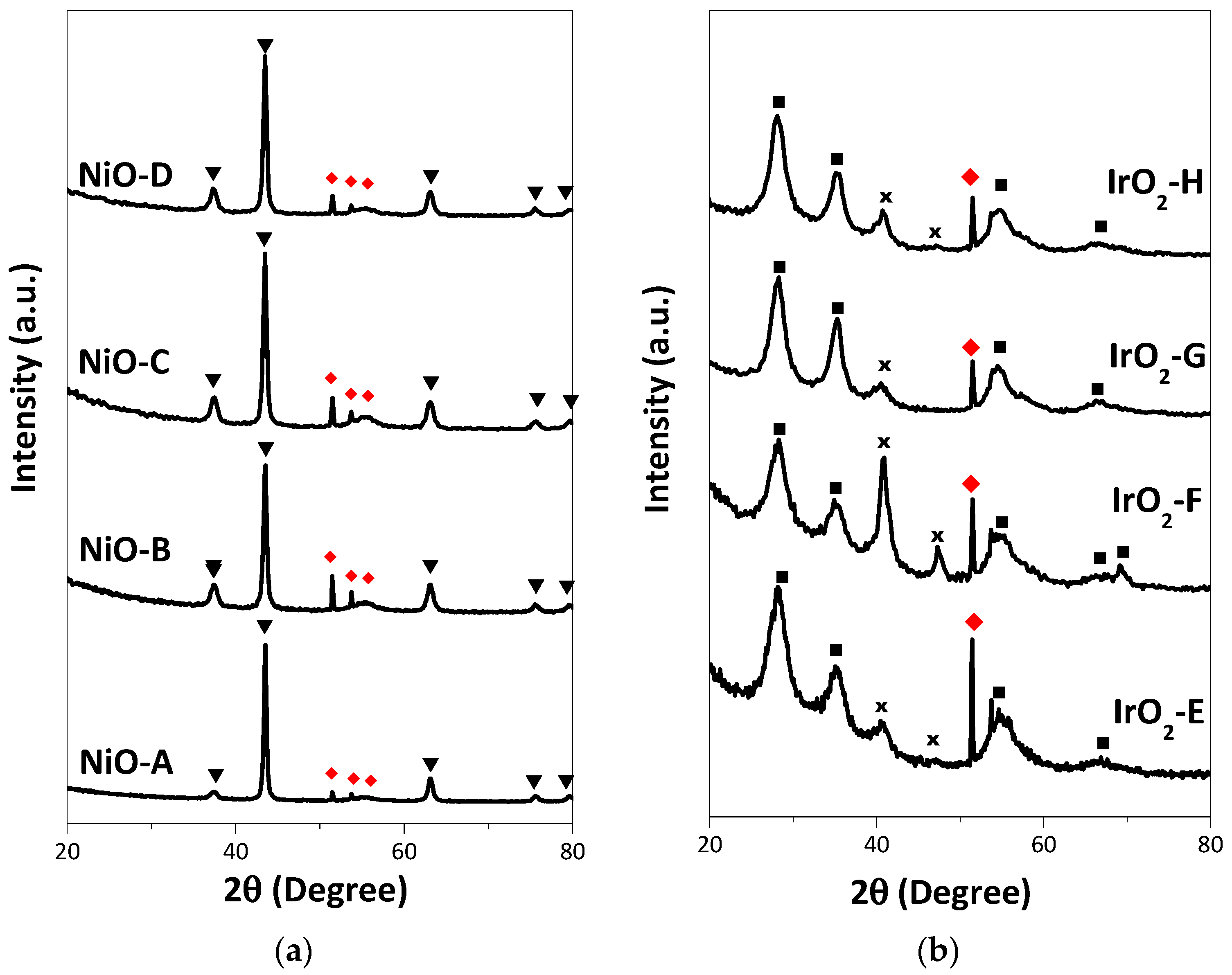
It can be seen from the GIXRD patterns in
Figure 4 that all of the as-deposited thin films were crystalline. Cubic NiO (JCPDS No. 01-073-1519) is the crystalline species detected from the NiO samples, while tetragonal IrO
2 (JCPDS No. 01-088-0288) and cubic Ir (JCPDS No. 03-065-1686) are the crystalline species detected on the IrO
2 samples. Generally, from the GIXRD patterns, the crystallinity of the materials was not significantly affected by the change in the sublimation and deposition temperature. In particular, IrO
2-F shows an increased intensity of metallic Ir (111) on the GIXRD patterns compared to the other samples.
The growth rates per cycle of the films (Å/cycle) are calculated from the film thickness and presented in
Table 2. The growth rate of the NiO films deposited at 200 °C is 0.2 Å/cycle, which is similar to the results reported by Hagen et al. [
14]. Meanwhile, it can be noted that the IrO
2 growth rate increases with increasing deposition temperature up to 0.6 Å/cycle at 210 °C.
2.3. Precursors Pulse and Purge Length
The precursors (Reactant A) used in this study were Ni-bis-2,2,6,6-tetramethyl-heptane-3,5-dionate (Ni(tmhd)2) for NiO and iridium (III) acetylacetonate (Ir(acac)3) for IrO2. These precursors were placed in open glass boats within the reactor, and N2 was used as a carrier and purging gas. Ozone (O3) was used as the oxygen source (Reactant B), which was supplied by the ozone generator near the ALD reactor (see more details in the Materials and Methods section). As mentioned in the previous section, one ALD reaction cycle consists of four steps that involve Reactant A and B pulse and purging.
The length for the precursor pulses and the inert gas purges needs to be optimized to avoid either too long processes or uneven films.
Table 3 summarizes the pulse and purge rates of Reactant A and Reactant B used in this study.
The growth behavior can be analyzed from the relationship of the pulse length versus growth per cycle (GPC). For the NiO samples, the same precursor pulse and purge rates were applied according to the study previously reported by Hagen et al. [
14]. When NiO films were grown using a precursor pulse length of 2.5 s, a similar GPC value of about 0.2 Å per cycle (
Table 2) was measured. Therefore, these conditions were chosen for this study. While for IrO
2 films, Hämäläinen et al. [
6] reported that a constant growth rate of about 0.4 Å/cycle is achieved with 0.5 s and longer Ir(acac)
3 pulse lengths. The effect of ozone pulse length on the growth rate is that the growth rate saturates to 0.4 Å/cycle when 0.5 s and longer pulses of ozone are used. Therefore, good saturation with respect to both the precursors has been obtained as a characteristic of ALD for all the depositions of this study.
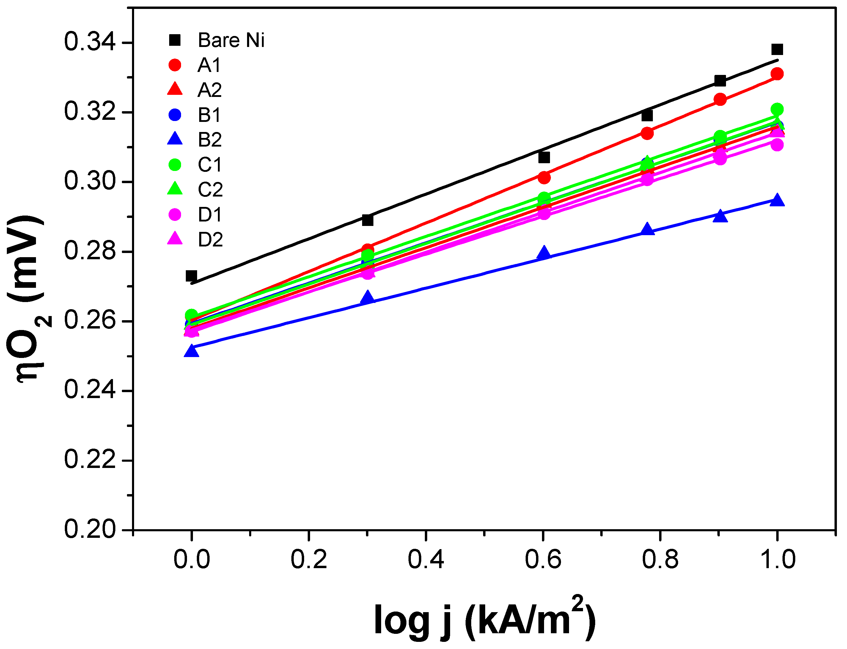
2.4. Electrochemical Characterization
In order to evaluate the electrochemical activity of the synthesized thin film electrodes, chronopotentiometry steps (1 to 10 kA/m
2) in a three-electrode glass electrochemical cell were performed, and the
iR-corrected single electrode potential (
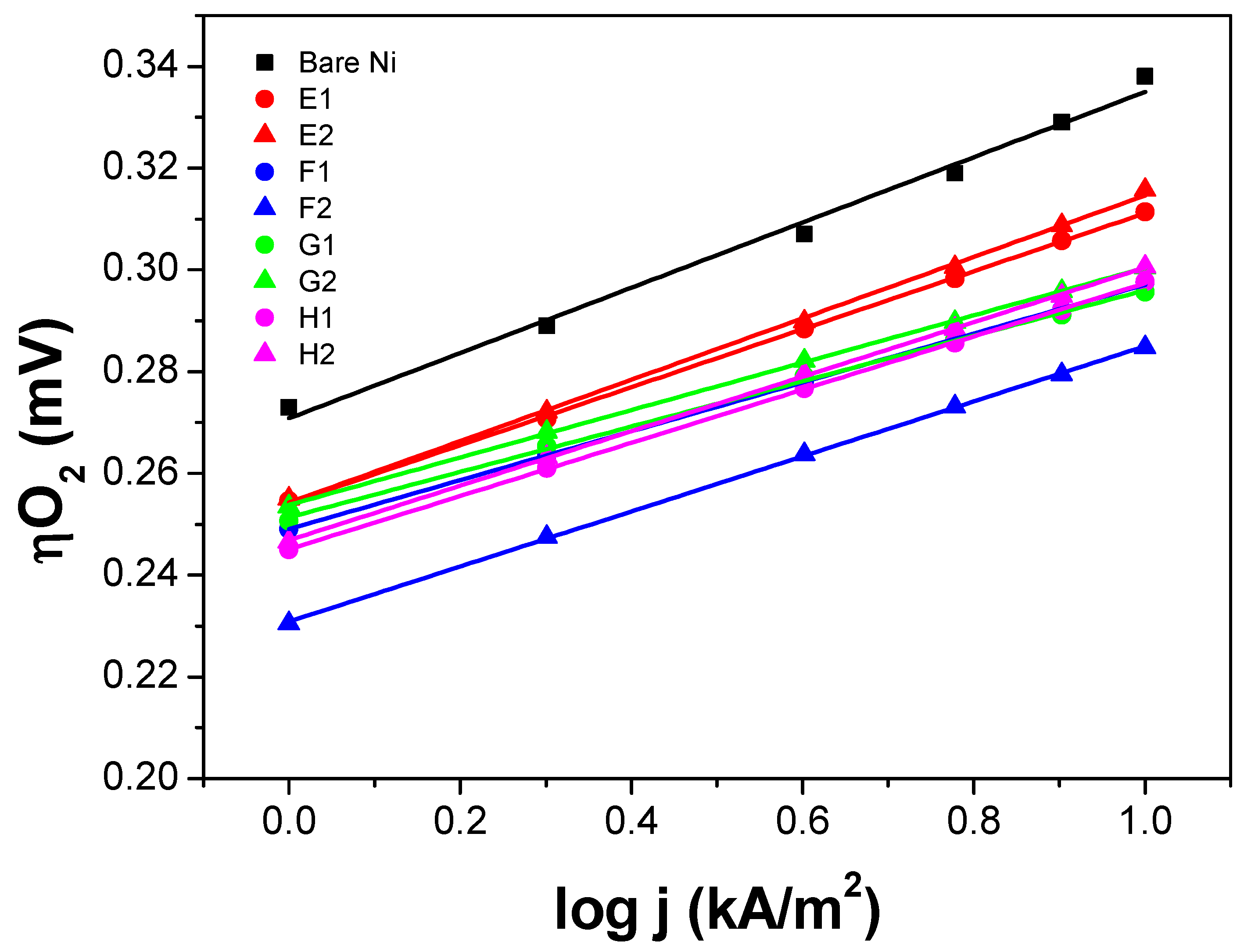
iR-SEP) was measured. All the measurements were done in 6 M KOH, 80 °C, and continuous agitation. The polarization curves shown in
Figure 5 and
Figure 6 were
iR-corrected and calibrated against a reversible hydrogen electrode (RHE).
The polarization curve of the uncoated Ni expanded mesh (black square) is also included in
Figure 5 and
Figure 6 to determine the voltage advantage in terms of mV-gain for all the thin film electrodes synthesized. Since for the industrial application, it is necessary to run the electrolysis system at the lowest power consumption as possible and given that the next generation alkaline water electrolysis will operate at current loads around 1000 mA/cm
2 (10 kA/m
2), the focus of this study is to compare the oxygen overvoltage (ηO
2) at such high current density. From the graphs, it can be seen that for the NiO samples, the oxygen overpotential (ηO
2) values at 10 kA/m
2 are approximately 10 to 50 mV lower than those of the bare Ni substrate. While for the IrO
2 samples, ηO
2 values at 10 kA/m
2 are approximately 25 to 55 mV lower than those of the bare Ni substrate.
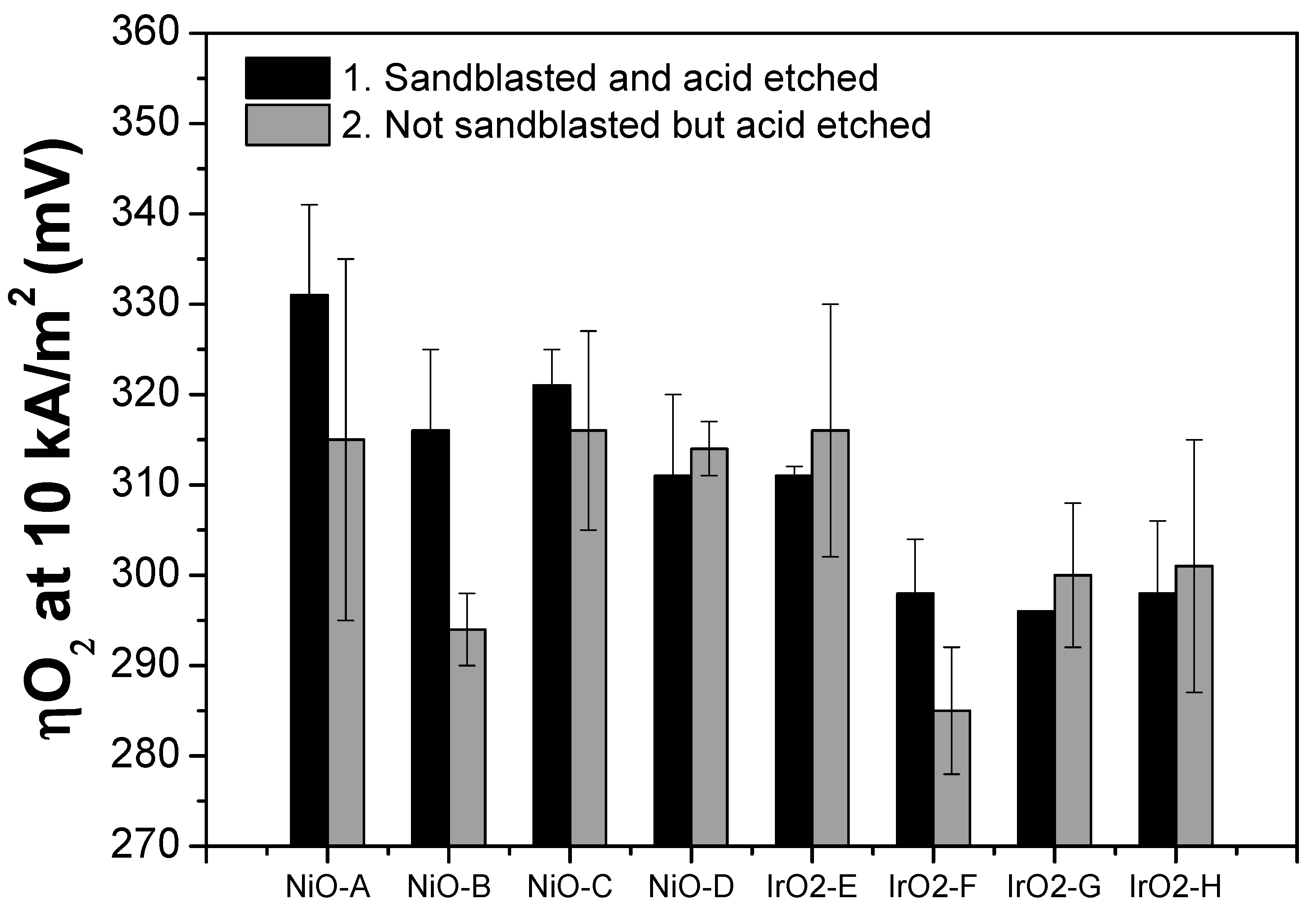
Table 4 and
Figure 7 summarize the ηO
2 values at 10 kA/m
2 for each thin film electrode. The Tafel slope of the thin film electrodes ranges from 42 to 70 mV/dec for the NiO samples and 45 to 60 mV/dec for the IrO
2 samples (see
Section 3 for more details).
For NiO thin film electrodes, it can be observed from
Figure 7 that samples with not sandblasted but acid etched Ni substrate have lower ηO
2 values than those of the samples with the sandblasted and acid etched Ni substrate. However, the opposite trend can be observed from the IrO
2 samples.
Table 4 summarizes the oxygen overpotential values at 10 kA/m
2 and the Tafel slope of each electrode material.
3. Discussion
As can be noted from the presented results, this study did not focus on the optimization of the ALD parameters, since these were already presented by Hagen et al. [
14] for NiO thin films and by Hämäläinen et al. [
6] for IrO
2 thin films. However, both the previous and current studies were able to show that thermal ALD can be employed for NiO and IrO
2 thin film deposition between the temperature range of 200 and 210 °C. These deposition temperatures were chosen to allow future studies where the co-deposition of IrO
2 and NiO can be done simultaneously, leading to a mixed oxide structure.
The film thickness depended linearly on the number of deposition cycles applied (shown in
Figure 1). Additionally, this study was able to show the uniformity of the thin films deposited based on different characterization techniques (SEM and XRF). From the XRF results, the front and back side of the electrode has relatively the same amount of iridium, which signifies the uniformity of the coating. Moreover, based on the GIXRD analysis, all the as-deposited thin films were crystalline. Other important ALD parameters are the pulse and purge rates of the precursors. It can be seen from the results that full saturation was achieved because of the application of the same operating conditions from the previous study and the use of small substrates. However, for an industrial-scale setup, this would not be the same case. The larger surface area of the substrates would require longer pulse and purge times to achieve full saturation. The problem can also be addressed through the application of batch processes where multiple batches of the substrates will be deposited simultaneously [
15]. In addition to the industrial scale-up of the process, there are some severe drawbacks of the technique, such as (a) the need of high-purity precursors that are not always commercially available; (b) the slow deposition rate, which is approximately 24 h total deposition time for the film described in this study; (c) the precursors are often sensitive to air/oxygen; and (d) expensive instruments. Nevertheless, a current industrial ALD instrument can treat substrates with a maximum dimension of 1 m
2. Finding the most suitable vacuum chamber for the deposition would be the major challenge to demonstrate the possible industrialization of the technique.
The focus of the study is the electrochemical application of these thin films as electrodes. Depositing uniformly such a small amount of materials (less than 1 g/m2 of metal) is a huge advantage for industrial scale electrochemistry, especially when a noble metal will be employed. Moreover, it has been proven that the small amount of materials deposited on the substrate resulted in electrochemically active materials for OER at strict industrial conditions (6 M KOH, 80 °C, up to 10 kA/m2). Oxygen overpotential (ηO2) values at 10 kA/m2 are approximately 10 to 50 mV lower than the bare Ni substrate for the NiO thin films, while they are 25 to 55 mV lower than the bare Ni substrate for the IrO2 thin films. These values correspond to energy savings in the industry especially when compared to the cost of materials employed. Comparing the ηO2 values of the NiO and IrO2 thin film electrodes, it can be seen that the IrO2 samples offered relatively higher mV saving than the NiO samples. For further study, the stability and lifetime of these electrodes should be explored.
One of the key points in this study that was not previously discussed deeply is the substrate pre-treatment. Two types of pre-treatment are applied on the Ni expanded meshes; one involves both sandblasting and acid etching, while the other involves only acid etching. Although both types of the pre-treatment method aim to increase the substrate surface roughness that subsequently improves the adhesion of the film, there are some differences in the characteristics of the materials. First, from the XRF analysis of the IrO
2 samples (
Figure 3), it can be observed that thin films deposited on the not sandblasted Ni substrate have relatively lower (darker) iridium content compared to the thin films deposited on the sandblasted Ni substrate. Then, this observation translates to the lower electrochemical performance of the samples with the not sandblasted Ni substrate (
Figure 7) compared to the ones with the sandblasted Ni substrate. However, the trend is the opposite for the NiO thin films, but these results agree with those previously reported study by Bocca et al. [
16]. Due to the limitations of the characterization techniques available, it is not possible to quantify the actual amount of Ni deposited on the substrate, but this could be more explored for further study.
Another observation is the relatively lower ηO
2 value of IrO
2-F among the set of IrO
2 thin films. This could be due to the presence of more crystalline metallic Ir, as can be seen from the GIXRD patterns (
Figure 4b). The XRF results also agree with this observation, as IrO
2-F has relatively more Ir content among all the IrO
2 samples. In addition to this, among the set of samples, NiO-A exhibits the highest ηO
2 value due to the low metal loading as well as low film thickness. Moreover, only one side of the substrate has been coated for these samples, which corresponds to approximately half of the total thickness of the other samples.
Figure 5 and
Figure 6 shows the polarization curves (Tafel plots) of the thin film electrodes, and
Table 4 summarizes the values of the Tafel slope. All the polarization curves of NiO and IrO
2 are shifted toward lower potentials compared to those of the bare Ni substrate, which leads to the lower ηO
2 values at 10 kA/m
2. Additionally, the polarization curves display steeper slopes (lower Tafel slope—except NiO-A) than that of the bare Ni substrate. The Tafel slope values are relatively similar ranging between 42 and 60 mV/dec, suggesting that the OER that takes place has the same reaction mechanism and fast reaction kinetics during the OER.
In summary, the study has demonstrated the feasibility of using the ALD technique to deposit conformal, uniform, and electroactive thin films on an industrially relevant metallic substrate as an anode for alkaline water electrolysis, which could be a source of hydrogen and is one of the promising sustainable solutions for the energy problem.
5. Conclusions
Thin films (approximately 25 to 60 nm) of nickel and iridium oxide were deposited on industrial metallic (Ni) substrates using the atomic layer deposition technique. Characterization of the NiO and IrO2 thin films showed the formation of a uniform coating. The as-deposited crystalline thin films showed good activity for OER especially at strict industrial conditions (high temperature, high pH, and high current density). Further study could be focused on the determination of the electrochemical stability of the materials, since this is one of the major requirements for industrial electrodes. Additionally, examining the adhesion of the coating could be a good measure of the lifetime of these electrodes. Furthermore, creating mixed oxide thin film electrodes could also be explored, as this will reduce the amount of noble metals that will be used.
Thus, ALD can produce active NiO and IrO2 catalysts that can be deposited as uniformed thin film coatings over industrially relevant metallic substrates. This offers a lot of advantages in terms of less usage of noble metals due to the nanometer-range film thickness. Similarly, ALD may be explored to produce other active and catalytic materials, and this work suggests that the ALD-deposited materials will have similar activity to films produced through other techniques. Hence, from this work, a promising route to manufacture an active thin film for sustainable H2 production was reported.


