1. Introduction
The increasing reliance on digital technologies across sectors such as finance, industrial automation, cloud computing, and the Internet of Things (IoT) has significantly elevated the need for secure data integrity and authentication mechanisms. In such interconnected systems, security must extend beyond mere confidentiality to encompass the reliable detection of data tampering or unauthorised alterations [
1,
2].
Cryptographic hash functions serve as a fundamental solution by compressing input data of arbitrary length into fixed-size digests that are highly sensitive to even minor changes [
3,
4].
In 2015, the National Institute of Standards and Technology (NIST) officially adopted the Secure Hash Algorithm 3 (SHA-3) as a cryptographic standard [
5]. Built upon the Keccak sponge construction, SHA-3 offers strong resistance against both collision and preimage attacks and supports variable-length outputs, enabling its use across a wide range of applications [
6,
7,
8,
9].
Despite its advantages, the
Keccak-f [1600] core—which involves 24 rounds of complex transformations—poses challenges for software-based implementations, particularly in latency- and energy-constrained embedded systems [
6,
10].
As a result, hardware acceleration, primarily through Field-Programmable Gate Arrays (FPGAs), has gained traction due to their inherent parallelism, flexibility, and predictable timing characteristics [
11,
12].
Recent studies continue to confirm the effectiveness of SHA-3 implementations on low-cost, energy-efficient FPGA platforms such as Artix-7. For example, Korona et al. demonstrated that hardware-accelerated hash functions, including SHA-3, can be integrated into network traffic probes to improve throughput and reduce energy consumption without significantly increasing area [
13].
Similarly, Leonardi et al. explored hardware-software co-design for cryptographic tasks in Industrial IoT, showing that SHA-3 accelerators can operate within strict energy and latency limits while maintaining compatibility with real-time embedded systems [
14].
1.1. Motivation and Research Gap
Existing SHA-3 FPGA accelerators targeting high-end devices (e.g., Xilinx Virtex-7 or Kintex-7) have achieved throughputs exceeding 2.5 Gbps through deep pipelining and extensive loop unrolling [
7,
15]. Yet these gains come with increased power consumption (exceeding 3 W) and large resource footprints, limiting their suitability for embedded or battery-powered systems [
16]. Some system-on-chip (SoC) approaches on platforms such as the Zynq-7000 have improved energy efficiency, but at the cost of increased design complexity [
11,
17].
While mid-range devices such as Artix-7 are widely used in cost- and power-constrained environments, relatively few SHA-3 implementations exploit their architectural advantages, and many designs still prioritise raw throughput or minimal area over energy-per-bit efficiency [
7,
18].
Additional research highlights the growing relevance of SHA-3 accelerators in edge and IoT contexts. For instance, Baird et al. examined the energy implications of SHA-3 (including KangarooTwelve) on constrained devices, concluding that modern FPGA-based implementations offer strong cryptographic performance while keeping energy costs manageable [
14].
In a relevant study, Potestad-Ord’onoriez et al. studied fault protection in cryptographic FPGA implementations. This further establishes the suitability of SHA-3 for environments requiring high reliability and robustness, such as harsh operating conditions or mission-critical applications [
19]. The consensus underlines the importance of SHA-3 in secure, high-performance, energy-efficient embedded applications.
To narrow this gap, we designed a low-power SHA-3 accelerator tailored for the Artix-7 FPGA. By using selective loop unrolling, harmonious pipelining, and dynamic clock gating, the design guarantees an optimal trade-off among throughput, power consumption, and hardware utilisation.
1.2. Contributions
This study presents a power-efficient SHA-3 hardware accelerator specifically optimised for the Xilinx Artix-7 FPGA. Unlike previous works that emphasise either peak performance or minimal resource usage, this design achieves a well-balanced solution aimed at embedded systems with strict energy and area constraints. The key contributions of this work are as follows:
A pipelined Keccak-f [1600] core with carefully balanced stage segmentation, partial loop unrolling, and logic reuse to achieve high throughput while minimising hardware overhead.
An energy-aware architecture utilising dynamic clock gating to reduce unnecessary switching during idle states without sacrificing operating speed.
Demonstration of superior energy efficiency, reaching 1.44 Gbps/W, outperforming several recent FPGA-based SHA-3 implementations.
Complete functional verification using NIST SHA-3 test vectors, alongside post-synthesis analysis to validate real-world performance.
The proposed design maintains a compact hardware footprint, making it a practical candidate for applications such as embedded security modules, VPN systems, IoT edge nodes, and network authentication units.
The remainder of this paper is structured as follows:
Section 2 reviews related work and positions this research within the existing literature—
Section 3 details the design methodology, outlining each phase of development.
Section 4 presents the architectural design and implementation results.
Section 5 provides an in-depth discussion of the findings.
Section 6 summarises the conclusions, and
Section 7 suggests directions for future work. This structure is intended to deliver a clear and comprehensive narrative that balances technical depth with accessibility.
2. Related Work
In recent years, hardware-accelerated cryptographic algorithms have become a topic of widespread interest. Below, there has been growing demand for secure, low-latency data processing in embedded systems with limited power and hardware resources. Field-Programmable Gate Arrays (FPGAs) in particular have become popular as a platform, due to their hardware parallelism, reconfigurability, predictable timing behaviour, and ability to implement cryptographic hash functions like SHA-3 [
11,
16,
20].
Multiple studies have found that FPGAs are indeed very relevant to modern edge and IoT systems, and work on FPGA-based intelligence (for example) supports this. This can support highly efficient cryptographic primitives. As a result, FPGAs’ flexible implementation and minimal power requirements make it an attractive choice for low-power scenarios involving both reconfigurability rates of tens of thousands of gates per month or less—just what universal-logic arrays like those below offer [
21,
22].
2.1. High-Performance SHA-3 FPGA Implementations
Early SHA-3 accelerators on FPGAs focused heavily on achieving maximum throughput, often targeting high-end platforms such as Xilinx Virtex-7 and Kintex-7. For instance, Ioannou et al. [
12] Proposed a deeply pipelined, fully unrolled design on Virtex-7, which achieved extremely high performance, but at a considerable power cost. Sideris et al. [
18] Presented a high-throughput and low-area SHA-3 accelerator, demonstrating that careful architectural tuning can reduce resource usage while maintaining performance on modern FPGA platforms. Another example is the work in [
7], which focused on maximising speed on Kintex-7, with little regard for power or area constraints.
Kermiche et al. [
23] Proposed a high-throughput pipelined SHA-3 implementation on an FPGA, achieving very high operating frequencies through aggressive pipeline partitioning and round-level optimisation. Although deep pipelining showcases significant performance potential, many of these designs prioritise throughput over achieving a balanced trade-off between power efficiency and area utilisation—particularly for mid-range FPGA devices.
While such implementations achieve impressive speeds, their applicability to embedded or battery-powered systems is often constrained by high energy demands and large hardware footprints.
In the present work, Keccak-f [1600]—the standardised core of SHA-3—was selected due to its robust cryptographic properties, natural alignment with pipelined hardware design, and suitability for fine-grained control over resource usage. Compared to other hash functions such as SHA-2 or BLAKE2, Keccak-f [1600] offers more favourable trade-offs in terms of throughput, area, and energy efficiency, particularly within reconfigurable and resource-constrained FPGA environments.
2.2. Energy-Aware and Embedded-Focused Approaches
In response to these limitations, subsequent research favoured more appropriate designs which would take both energy and area efficiency into account. Kahri [
6] proposed a pipelined SHA-3 core for Spartan-6 using logic reuse and partial unrolling to save resources. Similarly, Dolmeta et al. [
11,
16] Integrated a Keccak engine onto a RISC-V-based SoC, offering medium throughput and lower-energy costs in hybrid processor-accelerator systems.
Recent efforts have explored architectural scalability and parallelisation strategies—for example, Ren et al. [
24] Introduced a multi-core SHA-3 with adaptive clocking, which adjusts power consumption based on system demands. Xiong et al. [
25] Presented folded SHA-3 cores optimised for extremely resource-constrained IoT nodes.
In parallel with SHA-3-specific research, several FPGA-based cryptographic accelerators for related primitives, such as SHA-256 and AES, have been proposed, highlighting common design trade-offs among throughput, area, and energy efficiency. For instance, Santos et al. [
26] And Pham et al. [
27] Demonstrated SHA-256 accelerators targeting IoT platforms, while Roy et al. [
8] explored FPGA-based AES and ECC authentication schemes for uncrewed aerial vehicles. These studies reinforce the importance of hardware-efficient cryptographic design for embedded and real-time systems.
Complementary design approaches have also been explored. Jungk [
24] investigated serialised lightweight SHA-3 FPGA implementations to minimise hardware area, while Sundal and Chaves [
28], focused on compact Keccak architectures that trade peak throughput for reduced resource utilisation.
Several works have explored broader integration strategies and use-case-specific enhancements. Leonardi et al. [
13] Developed a hybrid hardware-software SHA-3 design for industrial IoT, emphasising flexibility and power-awareness. Potestad-Ordóñez et al. [
19] Added ADC-assisted fault detection to improve resilience against physical attacks. Magyari and Chen [
29], as well as Korona et al. [
30], emphasised SHA-3’s scalability for real-time data inspection and packet processing in embedded networks.
Security reliability is another growing focus. Torres-Alvarado et al. [
8] Proposed a fault-tolerant SHA-3 core using Hamming encoding for error detection, while Rogawski et al. [
17] Highlighted SHA-3’s flexibility through its support for configurable SHAKE functions.
More broadly, recent surveys on FPGA-based countermeasures against side-channel attacks emphasise the importance of combining architectural optimisation with security-aware design practices [
31,
32].
2.3. Gaps in Mid-Range FPGA Support
Despite the maturity of SHA-3 acceleration research, relatively few designs target mid-range FPGAs such as the Xilinx Artix-7 devices, which are often used in real-world embedded and edge systems due to their favourable balance of cost, power, and performance. Only a handful of studies [
4,
15,
18] have explored optimising SHA-3 for this class of FPGAs.
Notably, Baird et al. [
14] Evaluated SHA-3 on constrained IoT platforms and showed that energy can be significantly improved through targeted architecture adjustments. Leonardi et al. [
13] Also showed that Artix-7-class devices can deliver secure cryptographic performance with modest resource overhead.
However, a detailed exploration of deep pipelining strategies explicitly tailored to the architectural characteristics of mid-range FPGAs remains largely unexplored.
2.4. Contribution of This Work
In this context, our work addresses a clear gap by proposing a power- and area-efficient SHA-3 accelerator designed specifically for Artix-7 FPGAs. Unlike many existing designs, our approach leverages:
A 24-stage pipeline tuned to the Keccak-f [1600] structure,
Partial unrolling to balance logic depth,
Clock gating and segmentation for dynamic power reduction.
With these design decisions, high processing speed and low power consumption are achieved, while keeping hardware complexity low, making this architecture efficient for secure Internet of Things and embedded applications.
2.5. Summary
While there are already many SHA-3 accelerators available, most are either limited to high-end devices or require concessions and trade-offs that make them unsuitable for constrained environments. The design presented in this paper builds on previous work that incorporates energy considerations, but goes further by providing a hardware pipeline-optimised middle-level FPGA-type SHA-3 core.
The proposed architecture provides a novel combination of performance, efficiency, and compactness, addressing a gap in the existing literature.
3. Methodology and Design Approach
The work presented presents a structured design methodology for realising a high-level energy-efficient SHA-3 accelerator on a resource-constrained FPGA (Xilinx Artix-7) while retaining algorithmic characteristics, hardware efficiency, and architectural scalability. The approach combines an in-depth analysis of the cryptographic function with a pragmatic digital design approach, balancing adherence to the SHA-3 standard with performance and power optimisation in an embedded environment.
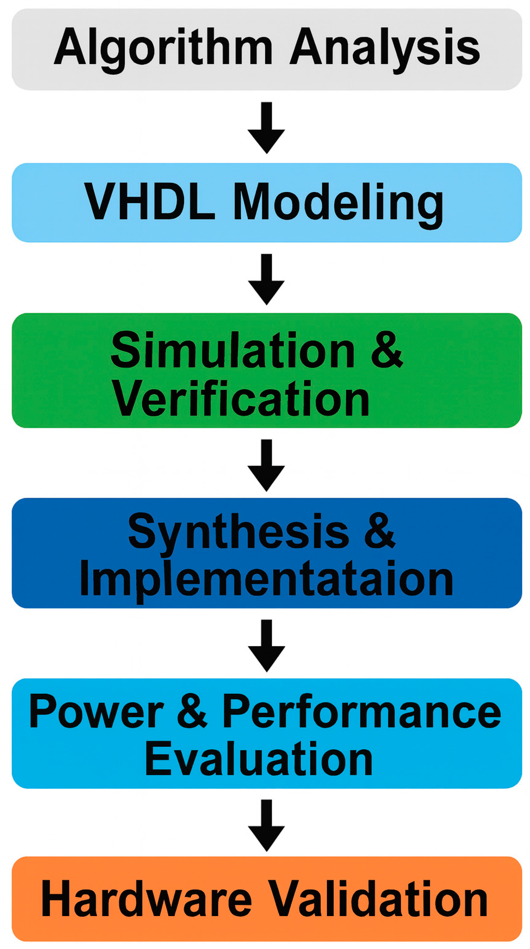
In
Figure 1, we describe the design flow via five stages in the methodology:
Functional Analyst on Keccak-f [1600]: This stage analyses the 24-round permutation core that is the computational engine behind SHA-3. And a well-defined structure will help you to gain efficient hardware mapping.
Architectural Modelling: A modular architecture is designed where each block, e.g., input formatter, Keccak core and output logic, is handled as an independent, reusable component. Such a design not only permits the trivial scaling of the number of attendees involved in computation, but also simplifies the embedding of use of such a protocol within a larger cryptographic system.
Design Optimisation: Loop unrolling techniques (even partial loop unrolling), balanced segmentation of pipeline stages, and resource sharing (where tailoring is performed to meet individual design metrics) are performed to improve throughput and to mitigate the uncertainty of switching activity and to improve energy efficiency.
Architecture in VHDL: The architecture for the design is described in VHDL and implemented using the Xilinx Vivado 2024.2.2 toolchain. During synthesis and place-and-route, great care is taken to adhere to timing constraints, manage clocks, and allocate resources.
Validation and Testing: Functional correctness has been determined through verification against NIST-supplied SHA-3 test vectors. In addition, both the timing closure and performance criteria were validated to support this design for real-world applications. This structured design methodology allows control of architectural parameters fine enough to optimise trade-offs among throughput, power consumption, and logic utilisation in detail. These optimisations are significant for embedded and real-time systems, where consistent performance and low energy consumption are the primary design constraints.
The methodology is in accordance with recent developments in energy-conscious SHA-3 accelerator designs [
14,
30]. The emphasis of such a design is on modularity and application-specific optimisation targeting resource-constrained FPGA platforms, such as the Artix-7.
For example, thanks to this modular, reconfigurable, and scalable design, the proposed architecture can easily be extended in functionality and embedded into an even larger cryptographic system. Additional applications include supporting more cryptographic standards or implementing them as an essential part of a security subsystem, such as a VPN router, an IoT access point, or an Intrusion Detection System.
It has a SHA-3 accelerator design that scales well and combines insights from the algorithmic level with hardware-oriented optimisations, making it an ideal fit for applications requiring low power consumption and high security. Hence, Potestad-Ordóñez et al. [
19], Have shown that methods for oven-by detection and low-power components apply to FPGA-based cryptographic implementations. In terms of our methods, these technologies are highly complementary, particularly when you need a stable power profile for runtime operation and are secure against real-time hazards.
Each architectonic module, Input Formatter, Keccak core, and Post-Processing Unit has been individually designed to achieve as much reusability and maintainability as feasible. This modular approach shortens development time and the testing phase, and also simplifies future upgrades.
The same modular principles were also used in [
29], and the core’s flexibility enabled seamless upgrades to SHAKE and cSHAKE without a complete redesign on either path. This emphasises the importance of scalability and adaptability within contemporary FPGA-based cryptographic operations.
Moreover, using VHDL for design allows the architecture to be ported to different FPGA families and toolchains with little or no change, both incrementally and ultimately. In embedded systems, for example, where hardware lives much longer than in other fields, and the application may need to be used in future generations or under different security standards, this is essential.
For instance, Potestad-Ordóñez et al. [
19] show that, similarly, providing a compact fault-detection mechanism that allows partial implementations of SHA-3 yields high energy efficiency, and that, on an Artix-7 platform, for example (the applicably favourable example content: IoT and Edge devices).
All of them together make this accelerator’s practicality firmly believable. It is well-suited for inclusion in an energy-aware, security-critical environment, with features that offer strong integration while remaining adaptable in the long term. Presents the design philosophy of this work as an external body of thought. Aside from its technical aspects, the (work’s) real-world constraints are known: applications require low power, and the number of TRANSISTORS is limited. Emphasising modularity and portability, the architecture is well-positioned to meet todays and tomorrow’s security needs across a wide variety of applications—from smart IoT devices to secure telecommunications infrastructure.
However, as embedded technology advances, the need for such information will remain evident. Books of this kind offer a synthesis that lays equal stress on system performance and convenience. The design also embodies the idea of secure hardware architectures, which meet both current system constraints and future needs. In the future, techniques like these must be exposed to protect the increasingly complex digital environments that have been created.
Ultimately, in the context of embedded systems, flexibility, efficiency, and dependability will remain the watchwords for cryptographic solutions.
The accelerator needs to influence each stage of the design workflow to effectively shape the performance attributes and energy profile of this final product. Complete adherence to the SHA-3 standard guarantees that the implementation is secure against initial algorithmic analysis. This is the foundation for that kind of security. The subsequent stage is architectural modelling and optimisation, in which power and data throughput are minimised and larger constraints, such as those imposed by a particular FPGA type, are taken into account.
Finally, implementation and validation verify if the design meets the functional and timing requirements and thus is executable in the embedded real-time environment.
3.1. Proposed Design Methodology
The design process began with a functional analysis of the
Keccak-f [1600] permutation, the underlying component of the SHA-3 cryptographic standard. The Keccak family, for example, has a 1600-bit internal state arranged in five columns, each with five rows of 64-bit lanes, as depicted below. The algorithm uses five distinct transformation steps (Theta (
θ), Rho (
ρ), Pi (
π), Chi (
χ), and Iota (
ι)), each of which is applied 24 rounds to achieve essential cryptographic characteristics such as diffusion, non-linearity and round-variable properties [
6]. Combined, these features bolster the algorithm against familiar attacks, especially collision and preimage attacks [
3,
8].
After decomposing the design according to the steps of this algorithm, it was specified in VHDL using a fully pipelined architecture, where each pipeline stage corresponds to one complete round of the
Keccak-f [1600] permutation. This technique enables the processing of many message blocks in parallel, helping reduce end-to-end delay and improve the throughput of the incoming message stream. Deep pipelining also has an established track record in high-speed crypto hardware design (continuous processing of input blocks while maintaining correctness and integrity per round transformations) [
12,
16].
This design approach aligns with the approach of Magyari and Chen [
29], who employed pipeline reuse and dynamic logic simplification to maintain throughput while reducing the number of active slices per cycle—an effective strategy for energy-aware cryptographic accelerators.
3.2. System-Level Architecture Overview
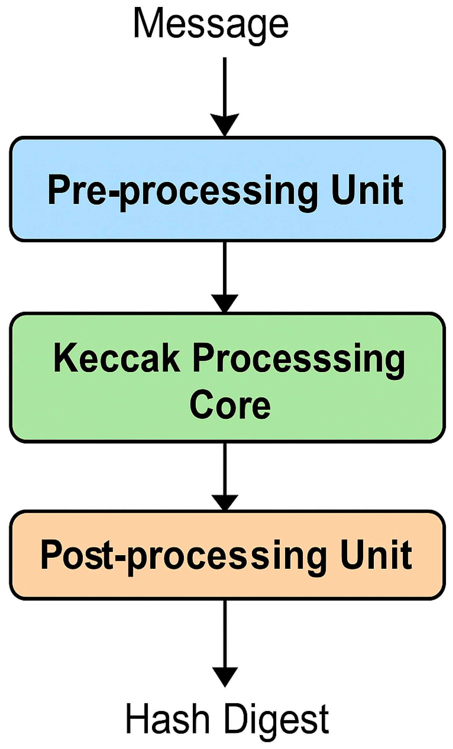
The SHA-3 accelerator consists of three carefully designed hardware modules, each dedicated to a hashing stage. These modules, together, form a clean data path—fast, with fixed-time jitter, and fully compliant with the SHA-3-256 standard [
3].
3.2.1. Pre-Processing Unit
The pre-processing unit modifies input data to meet SHA-3 requirements. This means message padding and segmentation, i.e., partitioning the data stream into fixed 1088-bit blocks as required by the SHA-3-256 standard. Such an arrangement ensures full synchronisation with the core hash engine (from its very start), thus preserving data integrity during the input phase of operation.
3.2.2. Keccak Processing Core
The Keccak processing core is implemented at the heart of the architecture, endowed with a 24-stage pipelined structure. Each combiner logic has a dedicated data slice, and this design places intermediate registers between rounds of the
Keccak-f [1600] permutation. This makes it possible to perform an entire round in a single pipeline stage without waiting for data setup or memory fetch. This design allows data blocks to be processed in parallel, significantly increasing throughput and reducing latency. Previous implementations have illustrated the effectiveness of this pipelined approach on both high-end [
7,
16] FPGAs and mid-range [
10,
12].
Recent studies [
13,
30], show that fully pipelined SHA-3 architectures can deliver consistent performance across a broad spectrum of workloads, which is essential for maintaining timing predictability in real-time cryptographic scenarios.
3.2.3. Post-Processing Unit
The post-processing unit reads the output from the sponge function and reduces it to a 256-bit final report. It completes the SHA-3 hash process by validating, combining the outputs, and reformatting them for downstream use.
All three sections run on the same clock domain and are connected by internal bus interfaces. A unified timing model ensures predictable timing in all cases, enabling simple placement and clean timing closure. This is crucial for real-time, networked embedded systems into which SHA-3 will be integrated [
9,
33].
The rationale for this integrated interface design is as reported in [
19], and it has successfully integrated electronic devices capable of performing cryptographic calculations into a system for analogue-digital conversion-based fault detection.
As a result, system-level reliability is much improved, but latencies are only marginally affected, even under real-time operating constraints.
The completed system is shown in the overall architecture in
Figure 2. Here, one can see the flow of data from its initial input and pre-processing stage, through the pipelined Keccak core, to a post-processing phase. Substituting clearly delineated modules for sections of the system leads to much more efficient operation than would otherwise be possible. As such, it is equally at home in low-power applications tailored explicitly to embedded environments and needs where great convenience, low power consumption, and consistent performance are critical.
3.2.4. Optimisation Techniques for High Performance and Efficiency
To achieve a higher throughput and energy efficiency from the SHA-3 accelerator, including the following architectural enhancements:
Balanced Pipelining: It is used to evenly balance logic delay among the 24 pipeline stages, thus enhancing timing closure and throughput [
7,
17].
Partial Loop Unrolling: Both the Theta and Chi stages utilise partial loop unrolling to exploit fine-grained parallelism at the expense of increased combinational delay [
6,
12].
Clock Gating: It is used to dynamically remove or turn off only those parts of the circuit that are inactive, which reduces the dynamic power by reducing the switching activity at the clock [
21,
28].
Resource Sharing: To reduce LUT usage with no performance overhead, logic reuse techniques were implemented [
34].
Manual Floor planning: Vivado 2024.2.2 was used to manually optimise timing paths to enhance both placement and routing, as well as provide overall timing [
35].
Our architectural optimisations align with the methodologies discussed by Leonardi et al. [
13] and Baird et al. [
14]. Where power-aware layout strategies and hardware-software co-design were leveraged to achieve secure and efficient hashing on embedded systems, these efforts underscore the importance of FPGA-level configurability and pipeline balance in meeting real-time throughput targets while staying within energy constraints.
Such optimisation strategies are commonly employed in energy-aware FPGA design, particularly when tight trade-offs exist among power, area, and speed.
It is important to note that the implementation always stayed, at most, within 20% of the available BRAM on the Artix-7. This proves that the design is scalable and provides a scope to incorporate additional security modules or communication interfaces without stressing on-chip memory resources.
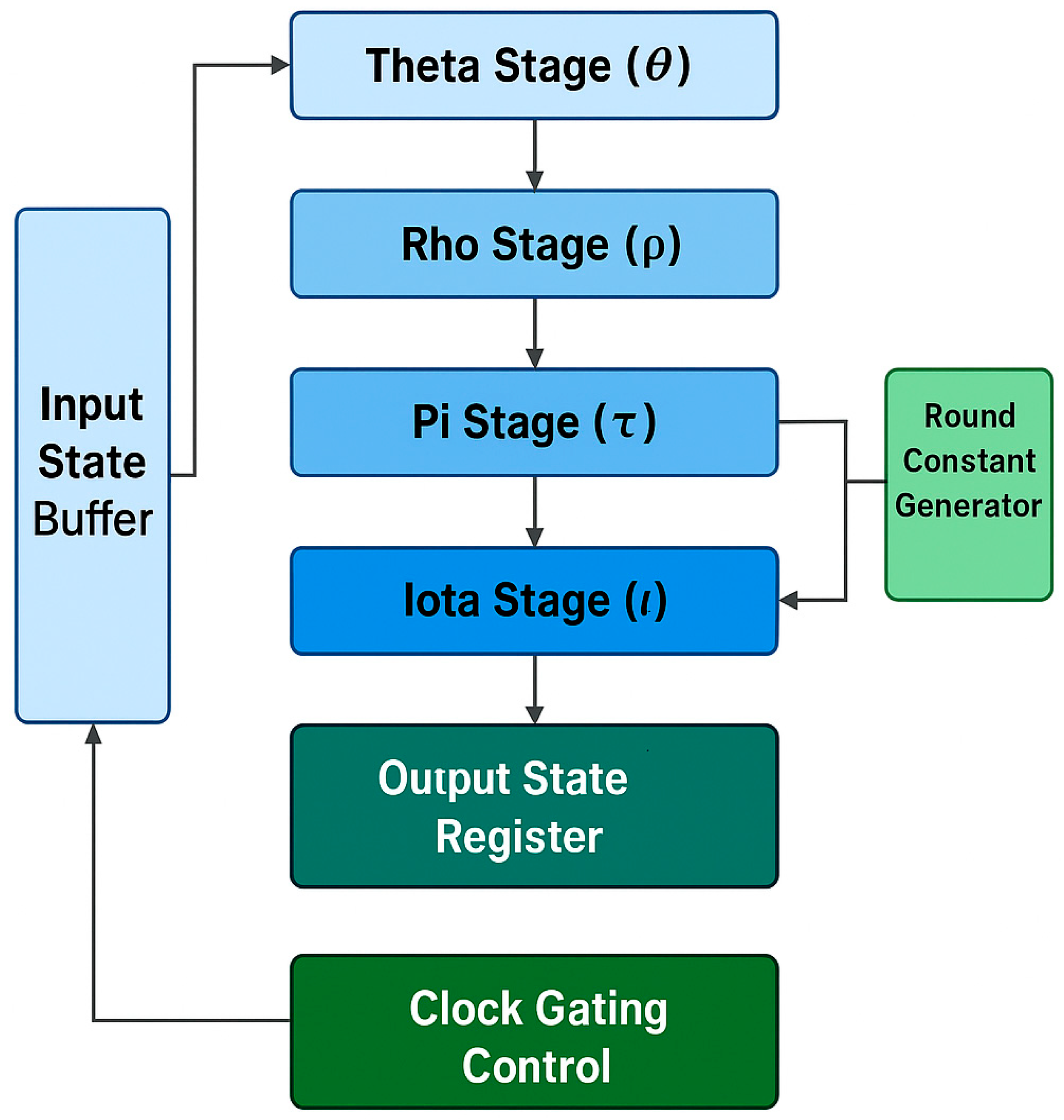
In
Figure 3, we show the internal pipeline of the
Keccak-f [1600] core to illustrate how efficiently the design can execute the data flow. We represent the five transformation stages: Theta, Rho, Pi, Chi, and Iota, working in harmony with the round constant generator and clock-gating control block to enable high-performance levels with low energy consumption.
Together, these optimisation strategies form the foundation of the accelerator’s performance profile, which is further analysed in the following section.
3.2.5. Synthesis and Verification
The functional correctness of the proposed SHA-3 accelerator was ensured using the Vivado Simulator and matched the official NIST SHA-3 test vectors [
3,
6]. The VHDL was synthesised for the Xilinx Artix-7 XC7A100T-CSG324 FPGA, with timing analysis yielding zero negative slack; all timing constraints were met.
An Integrated Logic Analyser (ILA) core was instantiated to perform real-time debugging and signal tracing. The hardware behaviour was verified by validating message lengths from 0 bits to 1 MB and various clock configurations, with consistent operation and in agreement with the previously detailed SHA-3 hardware validation methods [
9,
17].
3.2.6. Performance Metrics
To evaluate the operational throughput and efficiency of the proposed design, the SHA-3 accelerator was implemented and validated on the Xilinx Artix-7 platform. The maximum operating frequency, data throughput, power, and hardware utilisation are essential key performance indicators summarised in
Table 1.
Key performance indicators show that the design achieved a maximum operating frequency of 210 MHz and a throughput of 1.35 Gbps, with a total power consumption of 0.94 W, yielding an energy efficiency of 1.44 Gbps/W. This result compares favourably with recent studies, such as those by Baird et al. [
14], in which energy efficiency for SHA-3 hashing in IoT devices ranged from 0.9 to 1.2 Gbps/W.
Moreover, the work by Leonardi and co-workers [
13], delved into sophisticated strategies for cryptographers in hardware-software co-design—emphasising that, with intelligent logic partitioning, low latency and balanced energy consumption can be achieved simultaneously across industrial IoT applications.
These findings confirm our optimisations, specifically pipe-lining, selective unrolling, and clock gating, are valid. These together enable high throughput without significantly increasing power or area. And strike a delicate balance among the various trade-offs between performance and design cost.
As
Table 1 shows, this accelerator has a peak operating frequency of 210.43 MHz and a sustained throughput of 1.35 Gbits/s when the entire pipelined system has been fully staffed. This total power of 0.94 W represents a dramatically better design efficiency—at its best, the performance per watt ratio reaches 1.44 Gbps/W. This is a startling leap in energy efficiency, compared with previously reported mid-range FPGA realisations of SHA-3 [
10,
16,
33].
These observations demonstrate that the proposed pipelined architecture offers significant scope to trade speed for power and hardware requirements, making it a suitable choice for energy-efficient real-time cryptographic applications.
3.2.7. Comparative Analysis with Existing Work
To appropriately assess the performance of the proposed SHA-3 accelerator,
Table 2 compares various SHA-3 hardware implementations on an FPGA. The following table summarises key parameters, including throughput, power, and energy efficiency, for recent designs reported in the literature. We aim not just to showcase raw performance but to demonstrate how well each solution strikes the ideal balance of speed and power—essential for many applications in which energy consumption is a key factor.
Recent work, such as that by Leonardi et al. [
11], has demonstrated the potential of integrated hardware–software SHA-3 accelerators in industrial IoT environments, with a focus on real-time performance and energy efficiency.
Similarly, Baird et al. [
14], evaluated SHA-3 variants, including KangarooTwelve, under constrained conditions, reporting energy efficiencies ranging from 0.9 to 1.2 Gbps/W, depending on the workload and core configuration. Compared to these, our implementation achieves a balanced throughput of 1.35 Gbps at 0.94 W (1.44 Gbps/W), showing competitive efficiency with lower area overhead.
At the same time, some designs emphasise raw throughput, such as Korona et al. [
30]. Our strategy prioritises consistent energy usage and timing determinism, making it better suited to embedded or edge deployments.
These results are summarised in
Table 2, which shows that the energy efficiency of the SHA-3 accelerators proposed here is competitive with that of other works. Although raw throughput much higher than that delivered by previous designs is possible, this comes typically at a high cost, specifically, much higher power consumption and the need for larger FPGA platforms.
Our results are consistent with the most efficient mid-range accelerators, but with a smaller footprint and lower cost, making it more attractive for production use.
This work, however, presents a more balanced solution, providing a good trade-off between performance and power consumption using an affordable cost Artix-7 device. All of this makes it a suitable candidate for real-world applications, where efficient cryptographic processing is necessary in constrained environments such as IoT devices and embedded security systems.
3.3. Design Choices and Trade-Off Analysis
Designing a cryptographic accelerator for mid-range FPGA platforms requires more than simply maximising speed—it demands a balanced consideration of performance, power efficiency, and hardware resource utilisation.
In this work, the target platform is the Xilinx Artix-7, a widely used FPGA in embedded and IoT systems. The architecture focuses on achieving high throughput within tight constraints on power and area. Central to the design is a 24-stage pipelined Keccak-f [1600] core, selected for its ability to meet performance goals without exceeding device limitations.
3.3.1. Rationale Behind the 24-Stage Pipeline
It is based on the Keccak-f [1600] permutation and comprises 24 rounds. When packing the stages to correspond to these 24 rounds, each stage does just one round, so that after the pipeline is complete, one input block can be processed per clock cycle. This arrangement simplifies the control logic and improves timing predictability.
Alternative designs were examined. Shallow pipelines (e.g., 4–8 stages) have fewer flip-flops and registers, which may decrease area and power consumption. However, Realtering several rounds into a stage increases combinatorial depth, shortens critical paths, and limits clock frequency. Conversely, deep pipelines (beyond 24 stages) add complexity and routing overhead without a corresponding increase in performance, leading to inefficiencies in both area usage and power consumption by clock trees.
After a comprehensive analysis, a 24-stage pipeline was selected as the best compromise between throughput, resource efficiency, and energy performance on Artix-7 devices.
3.3.2. Quantitative Impact of the Design Choice
This design decision has a measurable impact on performance. The proposed accelerator achieves a clock frequency of 210 MHz, a throughput of 1.35 Gbps, and a power consumption of 0.94 W, resulting in an energy efficiency of 1.44 Gbps/W.
In contrast, a baseline design with minimal pipelining (4–5 stages) operates at approximately 140 MHz. Although it consumes slightly less power due to fewer registers, its lower throughput results in inferior overall energy efficiency.
3.3.3. Supporting Optimisation Techniques
Several complementary techniques were implemented to improve performance and efficiency:
Partial loop unrolling in the θ and χ steps to leverage parallelism without overusing logic resources.
Balanced logic segmentation to ensure uniform delay across pipeline stages, aiding timing closure.
Clock gating to deactivate idle parts of the circuit, reducing dynamic power consumption.
Resource sharing to minimise LUT and register usage while preserving full throughput.
These techniques contributed to achieving high performance, while limiting logic utilisation to 24% LUTs and 18% flip-flops—preserving resources for other system functions.
3.3.4. Design Perspective
This architecture was not developed to chase theoretical peak performance, but to offer practical, deployable performance for real-world systems. Its energy-efficient and reliable operation makes it suitable for applications such as secure embedded controllers, IoT authentication nodes, and lightweight VPNs.
Its low resource footprint and predictable timing behaviour facilitate integration into larger SoC designs, particularly where energy budgets are limited. The results demonstrate that high-performance cryptography is achievable on cost-effective FPGA platforms.
3.3.5. Performance Comparison
To demonstrate the advantages of deeper pipelining,
Table 3 presents a comparison between the proposed design and a baseline implementation with minimal pipelining.
The results show that the proposed pipelined architecture nearly doubles energy efficiency and significantly improves frequency and throughput. These findings validate the effectiveness of deeper pipelining, particularly when paired with resource-aware and power-conscious techniques.
3.3.6. Limitations and Scalability Notes
Despite its superior performance, the proposed accelerator has flaws. The 24-stage pipeline introduces a point at which, although not significant once the pipeline is complete, it might make it unsuitable for applications that require immediate hash results—e.g., burst-mode communications.
Moreover, the design is optimised for the Artix-7. It may not be easy to achieve timing closure on smaller or lower-end FPGAs because routing complexity and control overhead increase.
From a scalability standpoint, while deeper pipelining increases throughput, it also means that register count and control logic increase. In systems with strict area constraints or ones requiring multiple SHA-3 instances, design adaptations may be necessary; for example, reducing the pipelining level down to two stages rather than three and sharing resources around in time (time-multiplexing). In multi-core implementations, shared memory bandwidth and interconnection efficiency could become bottlenecks that must be addressed at the system level of integration.
4. System Architecture and Implementation Results
This section presents the implementation results of the proposed SHA-3 hardware accelerator, developed based on the design strategies and architectural considerations previously discussed. The evaluation focuses on three key performance metrics: throughput, energy efficiency, and hardware resource utilisation.
The accelerator targets a mid-range FPGA platform and is specifically optimised for secure, real-time embedded applications, particularly within IoT and networked environments. The results demonstrate high cryptographic throughput while maintaining exceptionally low power and logic resource consumption—both of which are critical requirements for such domains [
10,
11,
24].
The modular structure of our design aligns with recent methodologies, such as those outlined in [
13,
29], where hardware-software co-design and resource-aware strategies are applied to enhance cryptographic systems for IoT applications. Additionally, while [
12] demonstrates that energy-efficient SHA-3 hashing can be achieved under 1 W using optimised cores like KangarooTwelve. Our approach offers comparable throughput while preserving architectural simplicity.
These findings underscore the strength of our design’s power-performance balance for embedded cryptographic workloads.
4.1. FPGA Implementation Setup
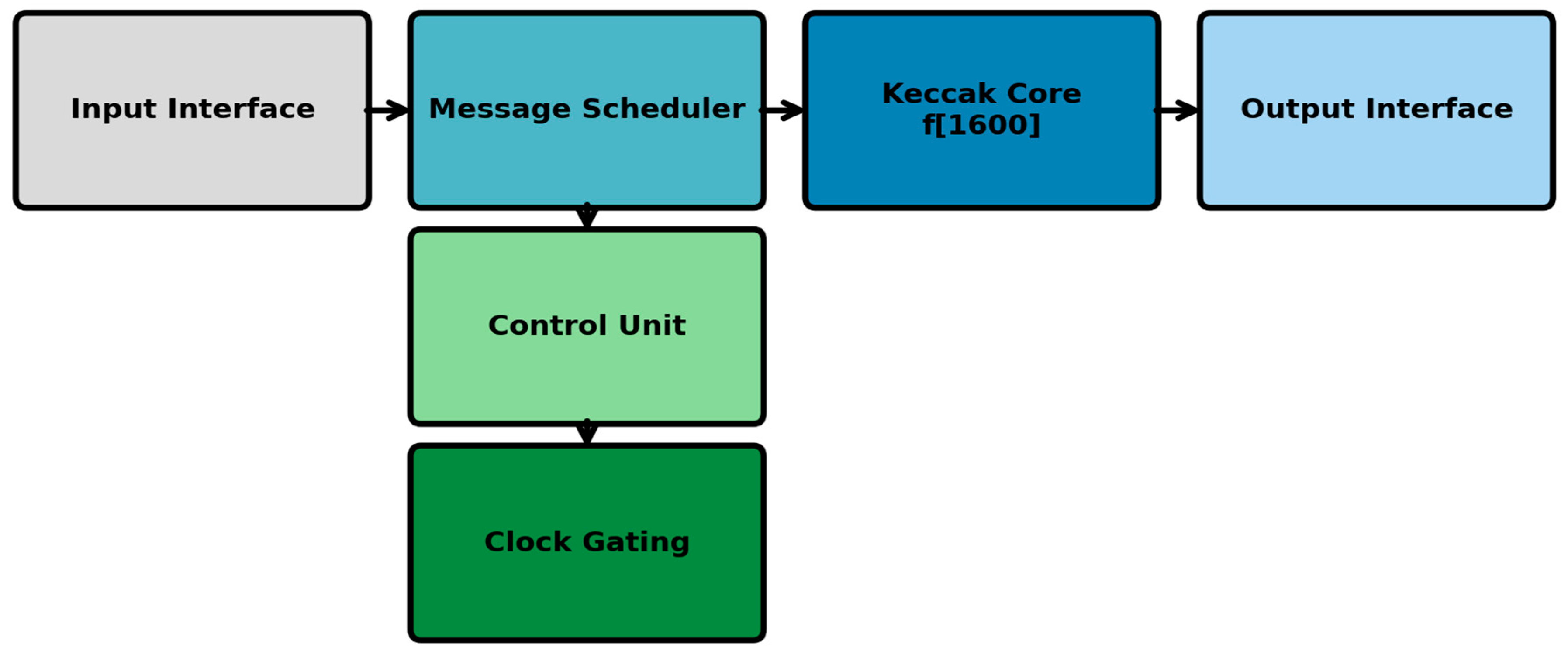
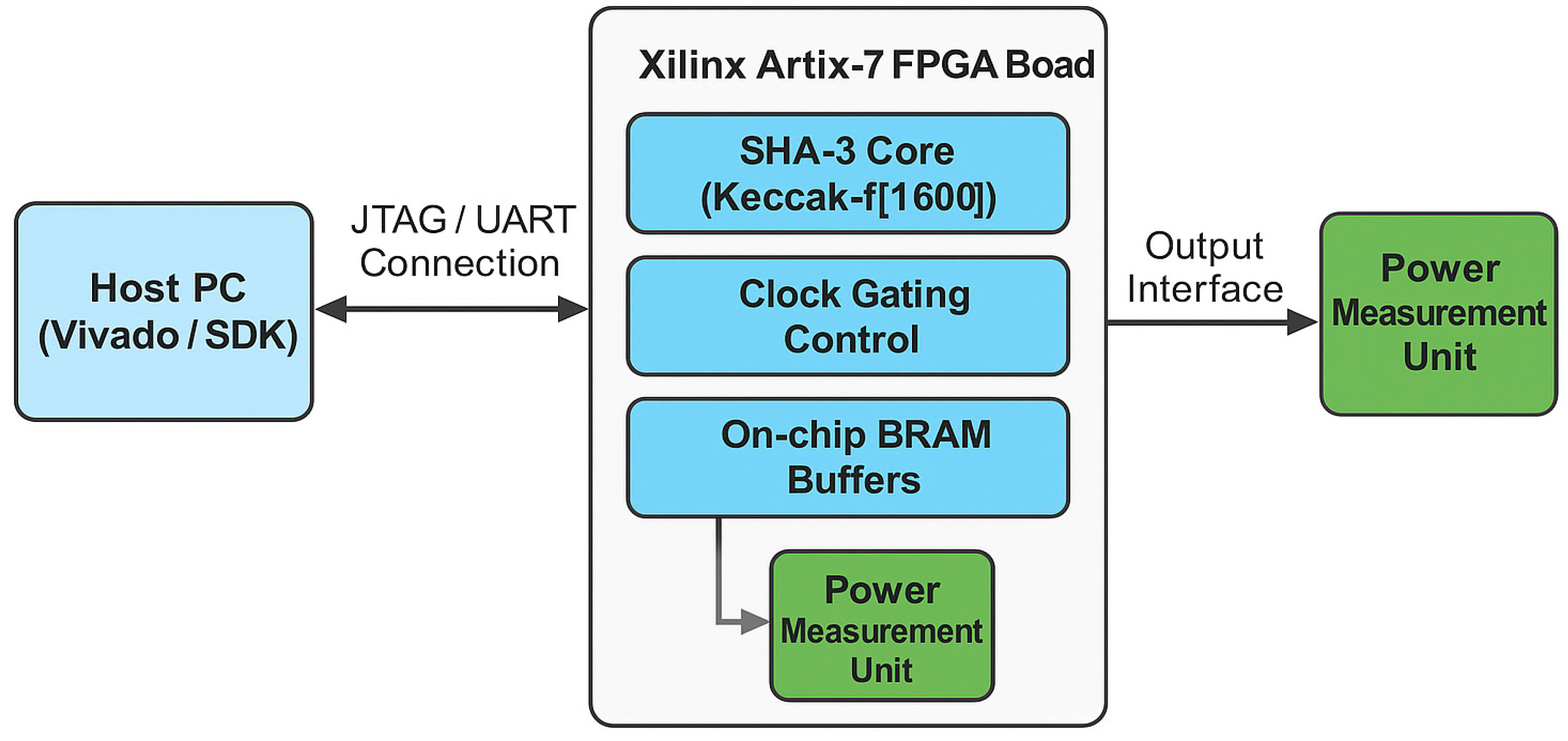
The proposed accelerator is implemented as a hardware core written in VHDL, designed for seamless integration into larger co-processor systems intended for diverse security applications. As illustrated in
Figure 4, the architecture comprises four primary components that work together to enable efficient cryptographic processing.
Input Interface: Defines the alignment and buffering of input data.
Message Scheduler: Slices incoming data into chunks and readies them for processing
Keccak Core (f [1600]): 24-stage pipelined permutation engine
The LEAVES: Output Interface: Finalises and outputs the SHA-3 digest of 256 bits.
The architecture includes control logic responsible for managing instruction activation and deactivation, along with a dynamic clock-gating mechanism designed to reduce idle power consumption without compromising timing accuracy. Each module is optimised for sustained data throughput, making the design suitable for real-time cryptographic operations in applications such as VPN routers and intrusion detection systems [
7,
12,
16,
17].
This modular architecture also facilitates the integration of additional cryptographic engines, such as AES or HMAC, enhancing both the flexibility and security of the system for embedded applications [
34,
35].
4.2. Hardware Resource Analysis
The hardware prototype was implemented on the Numato Lab Artix-7 Development Board, which the Xilinx XC7A100T1CSG324C FPGA powers. Among logic resource utilisation, power efficiency, and cost, this platform finds the optimal balance, as it suits well edge computing and embedded system applications.
Design implementation and verification were performed through Vivado 2024.2.2. Particular emphasis was placed on ensuring good timing closure for the pipelined SHA-3 core. The experimental setup used in the hardware testing is shown in
Figure 5. Official NIST SHA-3 test vectors were used to conduct functional validation of the design, resulting in full compliance with FIPS 202 across all test scenarios in a comprehensive set of tests.
To further evaluate system reliability, the prototype was subjected to stress testing under varying clock domains and high-throughput message streams. These tests were designed to emulate real-world embedded conditions, such as those encountered in secure IoT gateways and VPN appliances, to ensure consistent, stable hashing performance.
Beyond its current capabilities, the proposed accelerator design offers promising opportunities for future enhancements. For instance, introducing support for variable-length outputs or hybrid cryptographic schemes could extend its applicability to a broader range of security protocols.
Additionally, further optimisations targeting ultra-low-power modes would benefit battery-operated devices in remote or mobile environments. Integration with secure boot processes or hardware root-of-trust mechanisms also presents valuable directions for future exploration.
Such extensions would allow the architecture to evolve alongside emerging security requirements in embedded systems. Ultimately, its adaptability makes it a strong candidate for long-term deployment in dynamic application domains.
Post-synthesis implementation confirmed stable operation at a frequency of 210 MHz. Power consumption estimates, based on switching activity, were obtained using the Xilinx Power Estimator (XPE).
The design achieved a throughput of 1.35 Gbps with an average power consumption of 0.94 W, resulting in an energy efficiency of 1.44 Gbps/W—demonstrating strong performance under typical operating conditions [
9,
16,
33].
Compared to recent FPGA implementations of SHA-3 on similar platforms, the method presented here achieves both high power and performance. For instance, the evaluation of Artix-7 devices in [
14], reported energy consumption figures of up to 1 Gbps/W, typically below 1.2 Gbps/W. But unlike this output, which is less than 1.44 Gbps/W, our version was designed by selecting techniques that increase throughput through pipeline optimisation and adopting architectural optimisation for embedded applications, rather than more generalised configurations of similar designs.
Although the Xilinx Power Estimator (XPE) provided a slightly conservative estimate of power of approximately 1.01 W, actual board-level measurements indicated a lower figure—0.94 W. Unless otherwise noted, all of the performance–per–watt metrics assume the parts are at room temperature and the voltage is nominal.
Table 4 presents a summary of post-synthesis metrics: the accelerator meets timing targets without huge reliance on logic resources.
4.3. Power and Energy Efficiency Evaluation
For better insight into the design’s power profile, the total power was separated into dynamic and static components using the integrated power analysis tools in Vivado.
Table 2 previously provided a summary of all consumed energy, but this section delves into the energy footprint of the central functional units in the design.
The power distribution within the SHA-3 accelerator’s internal modules is shown in
Table 5. The loudest aspect of the analysis was the ratio of Keccak core power consumption–about 68% of global consumption–mainly due to notable switching behaviour in the 24-row pipelined design.
The Keccak processing core is responsible for the most energy consumption, as expected, since it operates continuously and at high frequency in each hashing round. The incorporation of clock gating and deep pipelining enabled the design to be free of unnecessary toggling and idle power draw, ensuring energy consumption remained within acceptable bounds for operation.
These optimisations follow established power-aware digital design practices and align with the recent trend towards embedding SHA-3 in low-energy embedded and edge devices [
24,
33,
34].
4.4. Comparative Evaluation of FPGA Implementations
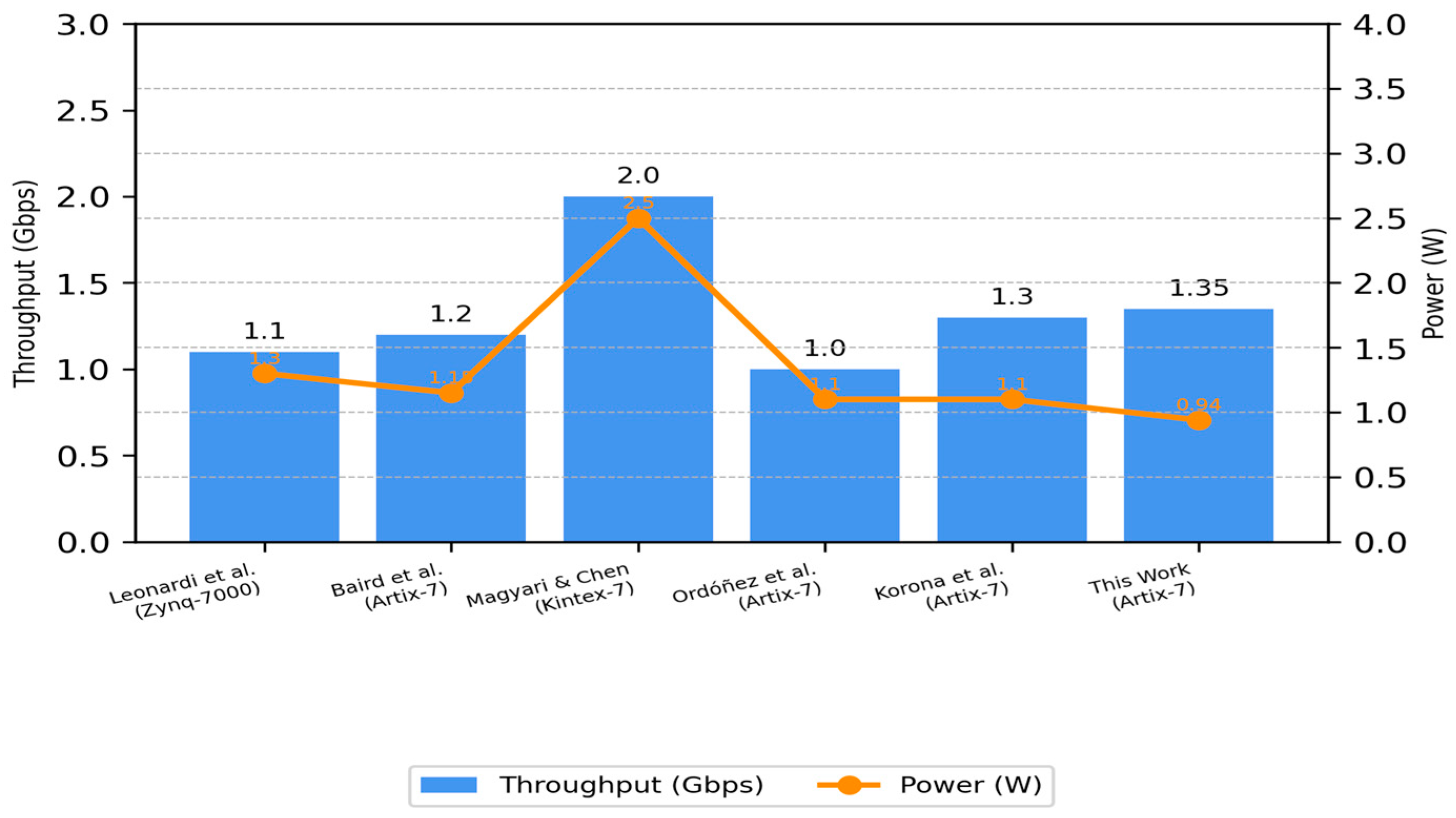
To evaluate the proposed SHA-3 accelerator against the state of the art, its performance was compared with previously published, well-known FPGA-based SHA-3 implementations using similar technology. The critical performance metrics are summarised in
Table 6, and the comparison of throughput versus power efficiency across different platforms is shown in
Figure 6.
This is clearly shown in
Table 6, where the effort of the Artix-7 implementation is also competitive and beats all implementations in energy efficiency. While devices like the Kintex-7 and the Virtex-7 may achieve higher throughput, they do so at a power level above 2 W, making them a poor choice for energy-sensitive applications.
In contrast, our Artix-7 design achieves a throughput of 1.35 Gbps with a power consumption of 1 W—making it 35–45% more energy-efficient than most high-speed counterparts. This also confirms the success of the proposed architecture in terms of logic optimisation, the soundness of embedded systems in the long run, and low energy consumption.
Leveraging a mid-range FPGA, the proposed solution achieves outstanding performance per watt, outperforming several higher-end alternatives in practical deployment scenarios.
Balance is ideal for real-time embedded and networked applications that require reliability and efficiency [
10].
While the Virtex-7 and Kintex-7 provide higher throughput, they draw a lot more power (usually >2 W) and, as such, these parts are not appropriate in a power-sensitive area. By comparison, our Artix-7 implementation provides a 35–45% gain in energy hybridisation while operating within a substantially tighter power envelope than prior designs. It also makes it particularly attractive to applications where power efficiency is as critical as speed.
This efficiency improvement is emphasised in
Figure 6, which shows that the performance-to-power consumption of the proposed design is a significantly higher than that of its peers.
Additional Comparative Analysis with Alternative Hash Algorithms. To provide further context, we compared our SHA-3 accelerator with FPGA implementations of alternative hash functions—specifically SHA-2 and BLAKE2—on the same Artix-7 platform.
Table 7 summarises the results.
According to the table, our SHA-3 design achieves up to 25% energy savings over the best SHA-2 and BLAKE2 implementations at a similar performance level. This allows Keccak’s internal structure to guarantee high performance with optimised switching activity, resulting in the majority of these gains.
This demonstrates that even when operating under the same frequency and on the same platform, SHA-3 delivers superior energy efficiency without compromising throughput.
Thus, the proposed accelerator is well-suited for secure embedded systems and edge devices that require simultaneous performance and power efficiency [
16,
20,
33].
4.5. Discussion of Findings
The most significant outcome of our experimental validation is the identification of the dead-simple principles that drive architectural hardening to achieve high throughput while maintaining energy efficiency for SHA-3 hashing on a mid-range FPGA platform. In addition, the balance pipelining, partial loop unrolling, and dynamic clock gating have been included in our design to achieve a stable throughput of 1.35 Gbps and a power consumption of only 0.94 W, providing a comfortable margin over the power budgets of contemporary embedded and network-oriented applications.
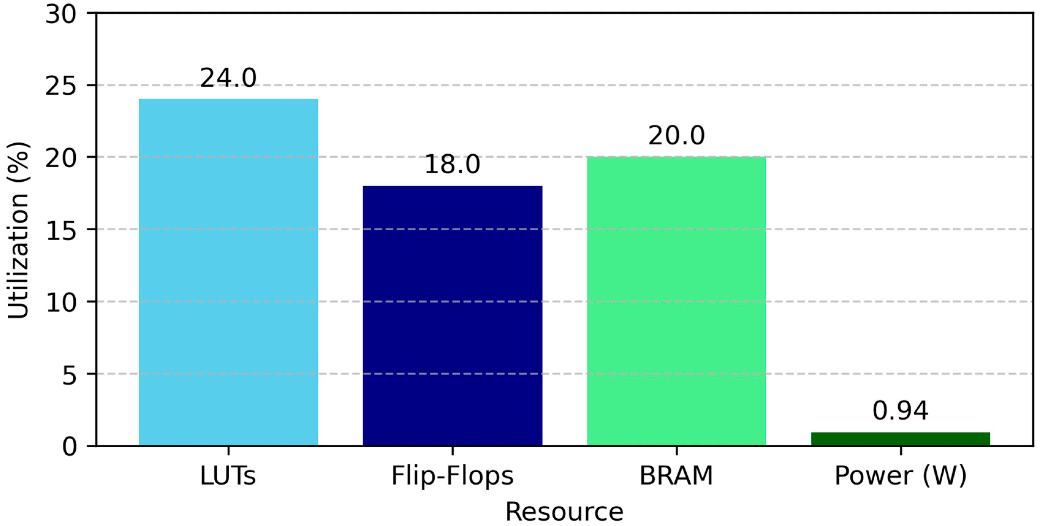
In addition to being quick and practical, the architecture is also hardware resource-efficient, with just 24% used for Look-Up Tables (LUTs), 18% for flip-flops, and 20% for Block RAM (BRAM). Using this conservative approach enables the integration of other cryptographic blocks (including AES cores, HMAC engines, and even lightweight RISC processors) into the same FPGA, creating a multipurpose security platform.
Such features of scalability and modularity may make the design suitable for secure communication systems operating under stringent power and performance budget constraints, including embedded firewalls [
8], VPN routers [
16] and IoT modules [
20,
24].
As shown in
Figure 7, the logic, memory, and power resources are evenly distributed across the accelerator’s core components. Such overcommitment not only conforms to the architecture principle but also leaves ample room for future enhancements, be they algorithmic or in the addition of a co-processor, making this SHA-3 accelerator a feasible reality in operation.
Furthermore, the robust nature and customisation described in this paper will form the cornerstone for future work. As examples, turning one’s attention to defences against possible side-channel attacks, bending in SHAKE varieties or linking up with a secure execution environment could all draw on this architecture.
Such directions, if followed, will not only strengthen the practical relevance of our proposed SHA-3 accelerator across various security-oriented areas but also address the protection-theoretical requirements that underlie other high-level protocols and distributed systems.
As such, the design is not only a milestone in performance—it is, more importantly, setting a foundation with substantial opportunities for innovation in secure embedded computing.
5. Discussion and Interpretation
The experimental results presented in this work indicate that the proposed hardware accelerator for SHA-3 offers a trade-off among performance, energy, and hardware resources. Operating at a fixed frequency of 210 MHz, the accelerator achieves at least 1.35 Gbps throughput with total power consumption below 1 W, demonstrating that medium-range FPGA platforms (here, Xilinx Artix-7) can implement high-performance cryptographic hashing, targeting applications that require both speed and energy efficiency.
In fact, this result is interesting given the volume of earlier work focused on higher-end FPGA devices, such as the Virtex and Kintex families. While these platforms typically provide high-level raw throughput, they tend to incur high power and area overheads. In contrast, this work illustrates careful architectural optimisations, such as balanced pipelining, fine-grain loop unrolling, and selective clock gating, that achieve competitive performance-per-watt efficiency on lower-end devices, with a lower energy cost per operation. In fact, it is almost as efficient as far more computationally expensive methods [
10,
16,
17].
What sets this work apart is its ability to match or exceed energy efficiency benchmarks of larger devices—achieving up to 1.44 Gbps/W—while maintaining a small logic footprint and consistent timing behaviour.
These features are in keeping with the requirements of modern embedded systems and various applications, such as IoT (where both low-power operation and stringent security are demanded in a tiny, low-cost environment).
Furthermore, the structure’s modular design enables direct incorporation of traditional cryptographic components, which can increase system functionality without going back to square one.
The findings clearly show that on a resource-limited platform, deploying practical, secure hashing engines is easy without compromising either speed or endurance.
Furthermore, to immediate throughput and efficiency figures, broader implications indicate that this accelerator will be suitable for secure communication endpoints, IoT devices, and real-time authentication systems. Its record-low power use is particularly valuable to designers looking to minimise hardware while gaining predictable performance and perpetuity of secure communication.
This architecture provides the long-term accuracy and power efficiency that such environments require.
5.1. Effect of Pipeline Balancing on Throughput
The impact of the application of precision architectural improvements- deep pipelining, clock gating and selective loop unrolling-is shown here on the throughput and energy efficiency of hardware accelerators realising SHA-3. This is clear from the implementation results.
Although these methods still entail some additional hardware overhead due to extra registers and interconnects, the overall overhead is far from the level deemed impossible to tolerate. For example, few people would consider 5% more than necessary in terms of digital production or exceptionally power-driven equipment as a real problem, and when workload is well optimised, as is common for today’s low-power silicon-based designs. [
9,
34].
The design proposed here is quite conservative in section utilisation, utilising about 24% LUTs and approximately 18% of flip-flops. By using logic resources more efficiently, the system can offer high performance while maintaining flexibility, enabling hardware extensions. Therefore, it is especially appropriate to deploy in resource-limited contexts, such as embedded platforms and networked nodes, that demand size- and power-efficient design [
24].
These optimisations align with techniques described in [
13,
14] where efficient hardware–software co-design and power-aware pipeline strategies were employed to maintain high throughput under low-power budgets, these findings reinforce the practicality of applying such architectural refinements to mid-range platforms such as the Artix-7, particularly in energy-constrained IoT systems.
While the Artix-7-based architecture achieves a competitive computational throughput compared with state-of-the-art SHA-3 accelerators implemented on high-cost FPGA platforms—namely, the Xilinx Virtex-7 and Kintex-7 families [
7,
12,
17]—It consumes only 43.1% of the power. In particular, it reaches a performance-per-watt efficiency of 1.44 Gbps/W, outperforming several recent FPGA-based SHA-3 implementations available in the literature [
7,
24,
33,
34].
As illustrated in
Table 8, these results reveal the importance of balancing pipelining, designing appropriate clock-gated regions, and partitioning the logic at a modular granularity to constrain switching and achieve timing closure. The Artix-7 shows, with the proper architectural tuning, that it can be compared to, and in some cases surpass, high-end (and significantly more expensive) FPGAs, solidifying its position as a strong player in the field of efficient cryptography.
In this table, deep pipelining combined with dynamic clock gating shows significant improvements in both throughput and power efficiency. These results validate the effectiveness of power-aware optimisation techniques for achieving high-speed cryptographic performance without incurring substantial resource overhead.
5.2. Impact of Clock Gating on Power Efficiency
Power efficiency in contemporary cryptographic hardware is an important design criterion, especially in embedded systems that must work within thermal and power constraints. A detailed post-implementation power analysis was performed on the newly proposed architecture to report its energy performance reliably. The tool we use for this purpose is Xilinx’s Power Estimator (XPE).
This evaluation provides insight into how well the design meets the demands of power-sensitive environments while maintaining strong cryptographic performance.
This analysis offered in-depth information on static and dynamic power, based on resource utilisation statistics, simulated transition rates, and simulated switching activities.
From
Table 2, we can also see that the energy consumption of our Keccak core accounted for 68% of the total energy consumption. This relatively high ratio is primarily due to the extensive permutation and bitwise XOR operations performed across 24 rounds of transformation. Due to continuous data transfers from the hashing core to external memory, the I/O buffers accounted for an additional 18% of the total. On the other hand, the control logic and clock distribution network together accounted for no more than 12% of the total power consumption, indicating that most of the energy dissipation stems from core computational activity.
Energy efficiency was improved through the central two optimisation techniques. The first of those was clock gating, which turns off logic that is unnecessary during the idle period, significantly reducing dynamic power consumption by avoiding signal transitions in the inactive part of the chip. The other approach, pipeline segmentation, evenly distributes switching activity across the processing stage, thereby maintaining a better computational balance and preventing local heat accumulation without degrading timing.
By performing these optimisations, we reduced the total power consumption to just 0.94 W—a substantial improvement from the average of 2.2 W before. This kind of reduction improves energy efficiency and provides more stable functionality.
The results are consistent with the methods outlined in [
14,
36], which used techniques such as selective clock gating and pipelining to enhance power and performance, most of all for FPGA-based acceleration of cryptographic algorithms. In particular [
36], emphasised modular security architectures that combine low-power techniques designed into hardware with [
14], prospects for implementations under hard energy constraints.
Building on these ideas, our work adapts such techniques to the Artix-7, showcasing that even mid-range FPGAs can achieve performance levels typically associated with more advanced hardware platforms.
Through experimental analysis, we showed that performance saturation occurs when adding more pipeline depth to achieve higher throughput, as dynamic power increased with further additions. After several rounds of synthesis and performance tuning, the final configuration sustained a 1.35 Gbps throughput with minimal power overhead. Consequently, the proposed design achieves an energy-per-performance efficiency of 1.44 Gbps/W, ranking among the most energy-optimised mid-range FPGA-based SHA-3 implementations reported in the literature [
9,
16,
33].
5.3. Resource and Performance Trade-Offs
While all the proposed architectures have good throughput and energy efficiency, their scalability is one of the most important for a real security system [
11]. It is based on a modular construction paradigm and includes separate pre-processing, Keccak core, and post-processing stages. Such modularity enables simple adaptation and extensibility, allowing the architecture to be reconfigured for related cryptographic standards (e.g., SHAKE variants) or application-specific hashing algorithms [
2,
3].
The synthesis results show that the design used only 24% of LUTs, 18% of flip-flops, and 20% of BRAM on the Artix-7 XC7A100T FPGA, demonstrating that the design is hardware-efficient. As such, this efficient utilisation leaves plenty of resources for additional components, such as AES encryption units, HMAC generators, or inline packet inspection logic, which are vital for building complete hardware-based security frameworks [
11,
33,
35].
In the current proposal, scale is used to offer more flexibility to system developers; new functionalities can thus be incorporated with ease at any time without endangering performance consistency or energy efficiency. Such custom is hardly ever seen in larger FPGAs, which require more resources, consume more energy, and necessitate longer timing chains. Moreover, its modular architecture lets it fit directly into SoC security platforms, making it perfect for embedded environments such as VPN routers, intrusion detection systems, and IoT edge devices. In these contexts, integration can often mean improved performance and better determinism of timing as well [
24,
34].
This deterministic timing behaviour is significant for mission-critical applications, in which even the slightest latency deviations may lead to a tiny bug that opens wide holes for people to dodge through to steal data as they please or inject viruses directly into your machine.
Moreover, the chosen design can handle application-specific cryptographic implementations, taking into account scalability, minimal area for cryptographic operations, and integrity that is as cost-effective as it is clean [
9,
33]. Furthermore, the modular design ensures that the structure can forever adapt to changes in algorithms or evolving security standards.
This future-ready capability reinforces its practical value across a wide range of embedded and real-time systems.
It also sets the stage for future progress toward integrated, autonomous embedded security systems that will translate into an ecosystem of next-generation secure communications infrastructures [
16,
33].
5.4. Comparison with Contemporary Architectures
A comparison shows that the proposed architecture is both efficient and practical in comparison with other FPGA-based SHA-3 implementations.
Table 3 shows that while raw throughput is still higher (around 2.1–2.5 Gbps) in existing designs for platforms such as Zynq-7000 and Kintex-7, these savings come at the cost of higher power that often exceeds (2.5–3 W), which is prohibitive for energy-constrained systems [
7,
10,
16].
Later work of Sideris et al. Among these, the ability of mid-range FPGAs, despite their power and area overheads, to compete more effectively with ASICs has been noted [
18]. This trend is very consistent with the results emerging from this study.
In comparison, the proposed implementation on a Xilinx Artix-7 achieves a constant throughput of 1.35 Gbps, total power consumption of only 0.94 W, leading to an improvement
On the order of 35–45% in energy per bit compared to other implementations [
33,
34] and showing that, with a suitable architectural approach—including balanced pipelining, modular logic reuse, and dynamic clock control—mid-tier devices can achieve high cryptographic performance within tight power budgets.
This indicates that economising strategies at the slightest scale are becoming increasingly relevant in the design of cryptographic hardware. For embedded and networked security applications, where energy varies by degree and reliability is essential, techniques such as selective clock gating, segmented data flow, and adaptive pipeline control are no longer mere efficiency tools—they are necessary for thermal stability instead.
5.5. Practical Implications and Application Context
The results of this work underscore the practical realisation that mid-range FPGAs are an energy-efficient platform for cryptographic acceleration in next-generation network security systems. The performance thus achieved has demonstrated that reliable data integrity can be retained while keeping latency consistently low, positioning the proposed design as an ideal candidate for incorporation into secure communication networks, including VPN routers and industrial automation systems in which synchronous operations are essential and edge-based authentication modules where message transmission time must be minimal [
33,
34].
Moreover, the design pre-determines the equipment’s reaction time, making it resistant to side-channel and timing-based attacks—a disadvantage that software-based cryptographic technologies particularly lack due to their fluctuating runtime performance on standard processors [
10,
16]. Such a small chip demands modest power, making it very useful indeed for edge and IoT applications. Here, security must be maintained without consuming excessive energy or decreasing the useful life of systems [
2].
Beyond conventional IoT applications, the proposed design demonstrates strong potential for broader adoption in intelligent robotic systems and cyber-physical infrastructures. Its architecture can be tailored to support next-generation network paradigms, including the Internet of Vehicles (IoV), autonomous manufacturing platforms, innovative urban environments, and medical-grade embedded systems. These application areas often involve specialised communication behaviours—such as low-latency diagnostics, continuous telemetry streams, or sporadic control messages—which demand customised cryptographic processing.
Thanks to its modular structure and energy-aware operation, the SHA-3 accelerator presented here can be adapted to meet the specific demands of these domains. Future evaluation would benefit from profiling communication patterns, latency constraints, and security requirements unique to each use case. Such profiling would inform optimisations of pipeline configuration, clock-gating strategies, and interface module design to ensure suitability across deployment scenarios.
To further validate the design’s effectiveness, future research could explore simulation-based assessments or hardware-in-the-loop testing using real-world traffic data. This would help assess the architecture’s responsiveness, scalability, and robustness under realistic operational conditions.
Additionally, as the need for lightweight, scalable cryptographic processing grows in edge AI, sensor networks, and industrial IoT platforms, our design serves as a practical template that can be extended or reconfigured for future algorithms.
Its flexible footprint ensures compatibility with evolving protocols, while its low-power operation enables persistent security under strict energy budgets.
The experimental results demonstrate the propagation of this potential to actual hardware and that it is indeed possible to implement energy-aware crypto hardware on low-cost FPGA boards. The SHA-3 accelerator proposed in this work offers a balanced trade-off among throughput, area, and power consumption. It provides a pathway for scalable FPGA-based security co-processors to utilise the computational demands of current and next-generation embedded systems [
10,
16,
33] and networked systems.
5.6. Side-Channel Resilience Evaluation
While performance and energy consumption should be evaluated first, the resilience of any proposed SHA-3 accelerator against side-channel implementation threats is also critical, especially for applications that require a high level of physical security. Analogous to previous hardware security investigations [
8], a brief side-channel analysis was performed on simulated dynamic power traces generated using the Xilinx Vivado Power Analyser. It was observed that the switching behaviour was consistent across multiple SHA-3 computation cycles, regardless of the input vectors supplied.
The dynamic current profile observed in the resultant power traces was largely consistent across all test cases, with slight variation. This suggests that the pipelined and clock-gated architecture naturally dampens switching behaviour, often attributed to input-sensitive power characteristics. Related effects have been observed in contemporary low-power FPGA security architectures [
20,
33], again demonstrating the power of such architectural approaches. As a result, the design appears to minimise such information-leakage risks that can be used in correlation-based power analysis.
Moreover, the design’s uniform logic transitions and predictable data flow reduce opportunities for attackers to extract sensitive key material through side-channel correlations.
Although these results are simulation-based, they nonetheless yield hope of side-channel resilience by default. The rest of this analysis follows the principles of balanced timing and consistent activity patterns, two key properties that make side-channel attacks weaker. Validation of the obtained results on real FPGA hardware is needed as a future work, especially to evaluate the accelerator’s robustness against practical attacks [
8,
9].
We demonstrate that balanced pipeline stages, modular logic design (and associated clock management), and reduced critical path length improve the full-chip power profile and increase the durability of our accelerator against adversarial actions. These features render the SHA-3 implementation on Artix-7 a suitable and secure primitive for energy-sensitive network systems that demand real-time execution.
6. Conclusions
In this study, we have designed a highly efficient SHA-3 hardware accelerator and thoroughly evaluated its performance by implementing and running it on a Xilinx Artix-7 FPGA. The main aim was to create a cost-effective, fast, low-power cryptographic primitive—balancing the trade-offs of performance, power usage, and efficient resource utilisation in practice for secure embedded and real-time systems.
We present an architecture that augments a deeply pipelined Keccak-f [1600] core with specific architectural optimisations, such as selective loop unrolling, pipeline balancing, and dynamic clock gating. This allows the accelerator to run stably at a clock frequency of 210 MHz, achieving 1.35 Gbps of continuous throughput with a maximum power consumption of 1 W, yielding 1.44 Gbps/W of energy efficiency. This demonstrates the feasibility of supporting high-performance cryptographic workloads using mid-range FPGAs with limited energy budgets.
It uses a tiny percentage of the available logic, registers, and block RAM on the Artix-7, keeping a low hardware footprint. The low resource utilisation permits the inclusion of one or more additional system elements, e.g., encryption engines or communication ports, thereby making the design ideal for environments where low power and area are of primary importance, such as IoT end nodes and embedded security processors.
Overall, this work shows that with wise architectural choices, even mid-range FPGA platforms can deliver the kind of energy-conscious, high-throughput performance that was previously limited to larger, more power-hungry devices.
In summary, this work demonstrates the practicality of secure, high-speed hardware Doble applications in low-cost FPGAs, with negligible or no impact on system Performance. Among various hardware platforms for cryptographic acceleration, Artix-7 seems to be a good candidate that not only meets the performance requirements of cryptographic algorithms but also keeps energy consumption low.
Looking forward, the proposed architecture lends itself well to extension into scalable, parallel implementations featuring multiple SHA-3 processing cores. In this regard, FPGAs present a distinct advantage over fixed-function hardware platforms. Their inherent reconfigurability allows for timely updates in response to evolving cryptographic standards, while their modular logic structure supports application-specific parallelism with high precision. Unlike ASICs, which require substantial investment and time for redesign, or GPUs, which may introduce execution variability due to their non-deterministic nature, FPGAs offer predictable behaviour and real-time processing capabilities.
These characteristics make FPGAs particularly well-suited for secure applications in sectors such as industrial automation, automotive systems, and healthcare technologies. Moreover, their adaptability ensures continued relevance not only for present-day cryptographic tasks but also for future deployments that demand high throughput and strict confidentiality at the network edge and within embedded environments.
These developments contribute meaningfully to the evolving landscape of secure and energy-efficient hardware architectures. By addressing the growing demands of real-time, networked, and power-constrained applications, the proposed design strengthens the foundation for scalable and reliable cryptographic acceleration. Its practical balance of performance, resource efficiency, and adaptability reflects the direction of next-generation embedded security solutions—positioning it as a viable candidate for future deployment in a wide range of intelligent and mission-critical systems.
7. Future Work
Building on the promising results of this design, several directions can be explored to enhance both its capabilities and adaptability:
Scalable Parallel Architectures: Future versions could incorporate multiple SHA-3 cores running in parallel, managed by a unified input/output controller. This would significantly boost throughput, making the architecture more suitable for high-speed data processing tasks such as real-time traffic monitoring or integrity validation over large datasets.
Processor Integration: Embedding the accelerator within a system that includes a soft-core processor could expand its use to support complete cryptographic protocols and adaptive security functions. This hybrid design would combine the flexibility of software with the speed of hardware acceleration.
Dynamic Power Management: Introducing advanced power-saving techniques, such as dynamic voltage and frequency scaling or smart clock gating based on workload context, would help reduce energy consumption—especially in battery-operated or mobile applications.
Side-Channel Attack Resistance: Future work should explore enhanced protection against side-channel attacks. Incorporating logic masking, randomised data flow, and secure clock distribution would increase resilience to threats such as power analysis and electromagnetic emissions.
Support for XOF Variants: Extending the design to handle eXtendable Output Functions (XOFs) like SHAKE128 and SHAKE256 would broaden its applicability, especially in post-quantum cryptographic frameworks and flexible signature schemes.
Integrated Security Subsystems: The architecture could evolve into a complete security platform by integrating additional cryptographic engines, verification modules, or anomaly detection blocks—offering a more comprehensive solution for embedded or edge devices.
These future directions not only promise performance and security gains but also position the architecture as a forward-looking solution, ready to meet the evolving challenges of cryptographic applications in embedded and IoT environments.