1. Introduction
The RFID assistive system represents a sophisticated integration of RFID technology and the IoT, aimed at enhancing the autonomy, safety, and quality of life for individuals with disabilities. For instance, an RFID navigation system is a key application that assists blind users in unfamiliar environments by providing vital orientation cues, thereby preventing accidents and promoting safe navigation [
1,
2]. These systems employ strategically placed RFID tags throughout public spaces, allowing visually impaired users to detect these tags using handheld or wearable RFID readers. This technology provides audible or tactile feedback, guiding users effectively while alerting them to potential hazards in real time. A notable innovation in this field is the RFID cane, which is equipped with a tag reader and antenna that emits radio waves to interact with nearby RFID tags, accurately pinpointing the user’s location [
1]. This enhanced mobility aid not only helps users navigate their surroundings but also fosters a sense of security and confidence. Furthermore, the RFID cane can transmit information via Bluetooth or ZigBee, enabling users to save destination names as voice messages, thus streamlining their travel experience and enhancing their ability to explore new environments independently.
Wearable devices that monitor vital signs and transmit data to healthcare professionals play a crucial role in supporting individuals with disabilities by ensuring timely medical assistance tailored to their specific health needs. RFID technology can enhance these devices by enabling precise tracking of users’ health metrics in real time, allowing for immediate intervention when necessary and thereby enhancing the overall well-being of disabled individuals [
3,
4,
5,
6,
7,
8]. Similarly, smart home technologies significantly improve accessibility for disabled users by automating daily tasks and enabling control through voice commands or adaptive interfaces. Incorporating RFID systems into smart home environments can facilitate seamless interactions between users and devices, allowing for personalized settings and efficient management of their surroundings. These technologies empower individuals with disabilities to manage their environments more independently, facilitating activities that may have previously required assistance [
1,
9,
10]. By leveraging RFID technology, these innovations not only empower individuals with disabilities to engage more fully in society by facilitating access to education, employment, and social activities but also streamline daily living, fostering a greater sense of autonomy and confidence that significantly enhances their overall quality of life.
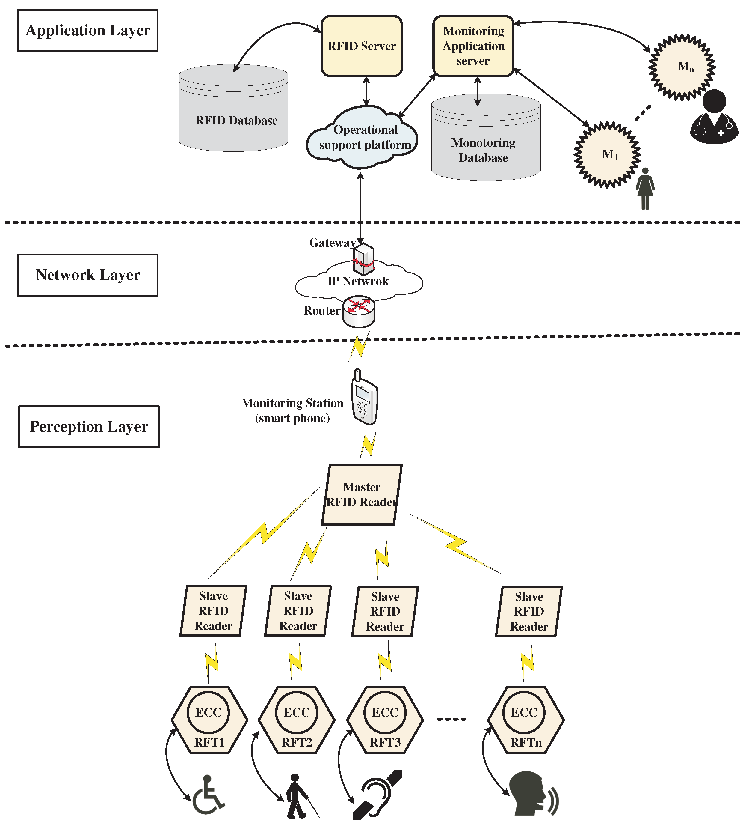
The RFID assistive system operates through a cohesive three-layer architecture that includes the perception layer, the network layer, and the application layer, as displayed in
Figure 1. Each layer plays a critical role in ensuring the system’s functionality, security, and adaptability to the unique needs of its users. At the perception layer, multiple slave RFID readers are strategically placed throughout various environments—such as homes, workplaces, and public spaces—to continuously scan for RFID tags worn by disabled people or attached to nearby objects. Each RFID tag emits a unique identifier when it comes within proximity of a reader, allowing for precise tracking of the disabled individual’s location and interactions with their surroundings. The master RFID reader collects data from all slave readers, aggregating this information to ensure comprehensive coverage and accurate monitoring of the individual’s presence and interactions.
The data are captured and transmitted to the network layer, which comprises a router, an IP network, and a gateway. The router connects the master RFID reader to the IP network, facilitating seamless communication between the various components of the system. This network enables the flow of data from the RFID readers to the operational support platform. The gateway plays a critical role in linking the IP network to this platform, ensuring that the data processed by the readers can be effectively accessed and utilized for further analysis. The incorporation of IoT technology allows for enhanced data transmission and remote monitoring, enabling continuous updates and real-time insights.
In the application layer, the data stored in the RFID database plays a vital role in the overall functionality of the system. This database not only stores information about the RFID tags and their associated disabled individuals but also facilitates data retrieval and analysis to generate actionable insights. The data are transformed into relevant information through a monitoring application server, which hosts applications designed to provide tailored assistance based on the unique needs of each disabled individual. For example, the system can provide auditory alerts to people with visual impairments when they approach obstacles or important objects, helping them navigate their environment safely. For those with hearing impairments, visual indicators or vibrations can signal important notifications or alerts in their surroundings. Disabled individuals with mobility impairments can benefit from the system’s ability to automatically adjust the environment, such as opening doors or rearranging furniture, to facilitate easier access and movement. Additionally, the system can assist individuals with cognitive impairments by offering reminders or prompts through various devices, such as smartphones or tablets, to help with daily tasks and routines.
The RFID server serves as a critical component in the application layer, managing the communication between the RFID readers and the operational support platform. It processes incoming data from the readers, ensuring efficient data handling and storage while facilitating the integration of various system components, thereby enhancing overall system performance and reliability.
The monitoring application server connects not only to disabled individuals but also to doctors, nurses, and caregivers, allowing them to stay informed about those they support. These healthcare professionals can access real-time data, receive alerts about unusual activities, and monitor the health and safety of their patients through a user-friendly interface on smartphones or tablets. For instance, if a visually impaired individual approaches a specific object, the system can generate auditory alerts or provide contextual information about that object.
Through its connection with IoT, the RFID assistive system can also connect to other smart devices within the environment. This allows for automated responses, such as adjusting lighting or providing notifications to caregivers when specific conditions are met. Overall, the RFID assistive system represents a comprehensive solution designed to enhance the safety and autonomy of individuals with disabilities. Additionally, it fosters a supportive environment by ensuring that caregivers and healthcare professionals remain informed and engaged in the care process. Through the seamless integration of data collection, processing, and application, the system guarantees that disabled individuals receive timely assistance tailored to their specific needs. This approach not only promotes their independence but also significantly improves their overall quality of life.
The RFID assistive system, while offering significant benefits to individuals with disabilities, presents several privacy and security concerns at each layer of its architecture [
11,
12]. Understanding these vulnerabilities is critical to ensuring user safety and maintaining trust in the technology. At the perception layer, eavesdropping emerges as a prominent threat. Attackers can intercept communication between RFID tags and readers, thereby exposing sensitive information regarding an individual’s location and activities. For instance, a visually impaired user utilizing an RFID navigation system may be subjected to tracking by malicious actors, leading to potential harassment or exploitation. The ramifications of such breaches are severe, as they undermine users’ sense of safety and independence.
Relay attacks represent another significant issue within this layer. In this scenario, an attacker employs two devices to extend the communication range between an RFID tag and a reader, misleading the system into believing that the user is situated in a different location. This deception can enable unauthorized access to secure areas or generate false alarms, resulting in confusion and potential harm, particularly for users with cognitive impairments who may struggle to process unexpected situations. For individuals with mobility impairments, being inadvertently directed into restricted areas can result in hazardous situations, especially in unfamiliar environments.
Denial of Service (DoS) attacks can significantly disrupt the functionality of the RFID assistive system. By overwhelming communication channels, attackers can render the system inoperative, depriving users of the critical guidance they rely upon for navigation. For example, if a visually impaired individual’s navigation system fails due to a DoS attack, they may become disoriented and susceptible to accidents. This scenario underscores their reliance on technology for safety, highlighting how disruptions can significantly impact their ability to navigate effectively and maintain independence.
Spoofing represents another significant concern at the perception layer, wherein attackers impersonate legitimate RFID tags. This fraudulent activity can cause the system to provide inaccurate information, thereby exposing individuals with cognitive impairments to misleading alerts or directions. Such misrepresentation may place these individuals in precarious situations, undermining their safety and autonomy.
While the perception layer faces substantial risks, the network layer is also susceptible to security threats that can compromise the integrity and confidentiality of user data. Man-in-the-Middle (MitM) attacks can intercept and alter communications between RFID readers and the gateway, jeopardizing the accuracy of the information transmitted. For instance, if health data from a wearable device is tampered with during transmission, it could lead to inappropriate medical interventions, thereby endangering the health of individuals with chronic conditions. Furthermore, data tampering within the network layer can compromise the reliability of the system. Unauthorized modifications to transmitted data could result in erroneous system responses, such as failing to alert caregivers during emergencies. For disabled individuals, especially those with mobility impairments, such failures can have severe consequences, including delayed assistance in critical situations.
At the application layer, security vulnerabilities can lead to severe privacy violations. Data breaches may expose sensitive information about disabled individuals, encompassing their health data and daily routines. Such breaches not only compromise privacy but can also result in discrimination or exploitation. For caregivers and healthcare providers, unauthorized access to the RFID database can lead to misinformation, resulting in inappropriate care or neglect. Additionally, malware attacks targeting the application layer can disrupt the monitoring application server, impairing its functionality or facilitating the theft of sensitive data. This disruption can prevent caregivers from receiving critical alerts or accessing real-time information about their patients, further jeopardizing the health and safety of disabled individuals who rely on timely interventions.
While security issues at the network and application layers are crucial, this study refrains from addressing solutions for these areas, as the existing literature has already provided a thorough exploration of various security measures and a comprehensive understanding of the related threats and mitigations. Focusing on the perception layer is especially urgent due to its direct impact on user safety and the immediate threats faced by individuals with disabilities. By prioritizing this layer, we aim to improve the security and effectiveness of assistive technologies that are essential for their safety and independence.
To mitigate cyberattacks targeting the RFID assistive system at the perception layer, significant efforts have been made to develop tailored security solutions. Advanced authentication protocols, particularly those employing ECC, offer enhanced security by leveraging strong cryptographic properties. However, implementing ECC on low-cost RFID tags is challenging due to the associated high computational demands, which often exceed the limited processing power, memory, and battery life of these devices [
8,
13]. In response, lightweight protocols utilizing simpler encryption methods have been proposed, but these solutions often exhibit vulnerabilities, such as susceptibility to impersonation and eavesdropping [
14,
15,
16,
17]. Recent innovations, including group authentication protocols compliant with established standards and schemes based on permutation matrix encryption, aim to balance security and efficiency for low-cost RFID systems [
18]. Despite these advancements, many solutions assume secure communication between servers and readers, which may not be feasible in mobile RFID contexts where communication channels are inherently less secure.
We have chosen to employ ECC in our RFID assistive system rather than adopting other recommended lightweight cryptographic standards such as ASCON and GIFT-COFB due to several compelling advantages [
19,
20]. ECC is recognized for its efficiency as a public-key cryptographic method that leverages the mathematical properties of elliptic curves over finite fields, providing robust security with smaller key sizes—typically 256 bits—equivalent to much larger keys in traditional algorithms like RSA. This not only enhances security but also reduces computational load, making ECC particularly suitable for resource-constrained environments where efficiency and power conservation are essential. Furthermore, ECC supports a comprehensive range of functionalities, including encryption, user and message authentication, digital signatures, and key distribution, which are critical for establishing trust and verifying identities in secure communications. In contrast, ASCON and GIFT-COFB are primarily symmetric algorithms focused solely on encryption and message authentication, lacking the versatility and broader application scope that ECC offers.
Table 1 presents a comparison of these algorithms to ECC; ASCON is an effective authenticated encryption algorithm that utilizes a permutation-based structure, while GIFT-COFB relies on a lightweight block cipher. While symmetric algorithms may provide speed advantages, they do not support the public-key functionalities essential for digital signature and secure key distribution. Moreover, every algorithm carries its own potential vulnerabilities: ECC may have potential vulnerability to side-channel-attacks if not implemented properly. Additionally, ASCON may be susceptible to collision attacks based on its hashing foundation, and GIFT-COFB may face challenges related to certain cryptanalysis techniques that its security are based on using light weight block cipher. Overall, the choice of ECC is driven by its superior efficiency, robust security, and ability to deliver a comprehensive suite of cryptographic functionalities essential for our RFID assistive system.
Implementing ECC-based authentication can significantly enhance the security of RFID assistive systems. However, deploying ECC on resource-constrained RFID tags presents several challenges. These tags typically have limited processing power, memory, and battery life, making it difficult to execute complex cryptographic operations efficiently. The computational overhead associated with ECC may lead to slow response times, increased energy consumption, and potential system failures, all of which are critical concerns for devices designed to support individuals with disabilities.
To address these challenges, a specialized hardware solution tailored for ECC can be developed. This solution would optimize the hardware architecture to accommodate the unique constraints of RFID tags while maintaining the integrity of cryptographic operations. The ECC algorithm primarily involves finite field arithmetic, with finite field multiplication serving as the foundational operation for various cryptographic functions, including field inversion and field division [
21,
22,
23,
24,
25,
26,
27,
28,
29,
30,
31,
32]. Therefore, finite field multiplication is a critical component of ECC, and its efficient implementation is essential for the overall performance and feasibility of cryptographic solutions on resource-constrained devices. Successfully implementing this operation on RFID tags is essential for the effective deployment of robust ECC cryptographic solutions. By optimizing this operation, it becomes feasible to execute ECC computations without overloading the limited resources of these tags. Traditional multiplication designs are often unsuitable for such devices due to their excessive area and energy requirements, which can hinder their practicality in low-cost, resource-constrained environments.
This work tackles these challenges by proposing an efficient and compact one-dimensional bit-parallel semi-systolic field multiplier optimized for the Montgomery multiplication algorithm, a widely used method in cryptographic applications. The proposed design significantly reduces both space and energy consumption while maintaining computational performance, making it well-suited for resource-constrained environments. By minimizing the area and power requirements of finite field multiplication, this solution enables the practical implementation of ECC on RFID tags, enhancing the overall security of the system. This strategy not only improves the security of RFID assistive systems but also ensures that individuals with disabilities can access reliable and effective assistive technology.
Based on the background provided, the remainder of this study will primarily focus on the design methodology used for implementing an efficient and compact finite field multiplier that supports the computational demands of the ECC algorithm. This makes it suitable for integration into resource-constrained RFID tags designed for individuals with disabilities. The ASIC implementation results presented at the conclusion of this study demonstrate significant improvements in key metrics, including area, power consumption, Power-Delay Product (PDP), and Area-Delay Product (ADP), ensuring compliance with the stringent requirements of low-cost RFID assistive devices while delivering robust security. This innovation has the potential to greatly enhance the safety and autonomy of individuals with disabilities, allowing them to benefit from secure and reliable assistive technologies in their everyday lives.
2. Literature Review
The effectiveness of finite field multiplications depends critically on the choice of base representations for the elements in GF(
). The advantages of other basis representations, such as Polynomial Basis (PB), Normal Basis (NB), Dual Basis (DB), and Redundant Basis (RB), are clear [
33]. When it comes to these representations, polynomial basis arithmetic stands out as a simple, reliable, and scalable method, especially for hardware implementation [
34,
35,
36,
37,
38]. Polynomial basis arithmetic is commonly used in cryptographic protocols because it does not require basis conversion, unlike other representations. The effectiveness of finite field multipliers is greatly influenced by the irreducible polynomial chosen. All-Ones Polynomial (AOP), trinomials, and pentanomials are a few examples of irreducible polynomials that are employed in cryptographic techniques. Despite the fact that trinomial and pentanomial-based multipliers are more efficient, generic polynomial-based multipliers are still useful for a variety of applications. Although irreducible AOPs are not utilized as often as irreducible trinomials or pentanomials, they still have the potential to design efficient multipliers [
39,
40,
41].
Different methods of implementation can lead to the creation of diverse multipliers with varying characteristics. Bit-serial multipliers are known for their space efficiency and significant power savings, albeit at the expense of slower operation, requiring
m clock cycles to multiply two elements [
22,
42,
43]. On the other hand, bit-parallel multipliers provide the advantage of producing results in a single clock cycle but come with higher hardware costs and power consumption [
24,
25,
28,
44,
45,
46,
47,
48,
49]. In the framework of Very Large Scale Integration (VLSI) implementations, systolic/semi-systolic serial or concurrent multiplier topologies are chosen over traditional approaches. This is because they possess qualities such as regularity, modularity, local relatively homogeneous connectivity, and concurrency, which make them ideal for VLSI designs. Furthermore, systolic/semi-systolic arrays have underlying pipeline properties that allow for high clock frequencies irrespective of substantial resource use.
Numerous researchers have made significant efforts to devise effective implementations of systolic/semi-systolic multipliers for binary extension fields GF(
). These studies primarily focus on constructing multiplier architectures using specific irreducible polynomials. For instance, Lee and Chiou introduced in their work an error-detecting semi-systolic array multiplier [
22,
50]. Huang proposed an efficient semi-systolic array multiplier aimed at reducing both time and space costs [
23]. In their work, Choi and Lee addressed the need for a highly efficient systolic array architecture that performs unified multiplication and squaring operations with minimal hardware overhead [
25]. They developed a serial and parallel systolic array that enables rapid modular exponentiation by concurrently executing multiplication and squaring operations. This architecture is designed to optimize performance while minimizing resource utilization. Moreover, the incorporation of LSB-first multiplication and exponentiation algorithms further enhances the efficiency of the systolic array, allowing for faster computation of modular exponentiation.
In a separate study, Chiou proposed a semi-systolic array multiplier that offers reduced time complexity [
51]. By carefully designing the multiplier structure, they achieved significant improvements in computational efficiency. This reduction in time complexity is crucial for applications that require fast and efficient multiplication, such as cryptographic algorithms. Recent research by Lee introduced novel semi-systolic Montgomery modular multipliers that leverage two levels of systolic computation [
52,
53]. These multipliers demonstrate efficient area utilization and reduced delay, which are essential factors in VLSI implementations. The utilization of systolic computation allows for parallel processing and pipelining, enabling faster and more efficient modular multiplication operations.
Mathe and Boppana proposed a multiplier architecture that supports both parallel and serial inputs [
54]. This architecture provides flexibility in handling different types of operands and allows for efficient multiplication and squaring operations. By accommodating various input configurations, the multiplier can adapt to different application requirements and optimize performance accordingly. Additionally, Ibrahim introduced efficient one-dimensional bit-serial and bit-parallel systolic array structures for multiplication and squaring operations over GF(
) [
32]. These structures are specifically designed for computations within the finite field GF(
) and offer efficient utilization of hardware resources. The bit-serial and bit-parallel systolic arrays enable optimized processing of binary data, making them suitable for applications such as error correction codes and cryptography.
In recent research by Pillutla and Boppana, a novel GF(
) polynomial basis systolic multiplier was introduced, specifically targeting field sizes
m = 233 and
m = 409 [
36]. The proposed architecture incorporates suggested trinomials to enhance its performance. While GF(
)-based multipliers have been created for a variety of applications, they frequently encounter difficulties owing to their high hardware complexity and large delay durations, especially in security-related applications. Therefore, it is crucial to conduct further investigations to explore multiplication architectures that can provide efficient performance while minimizing space and time requirements.
In the realm of bit-parallel systolic multipliers, a multiplier structure was initially proposed by Lee that utilized equally spaced and AOP polynomials as the foundation for its design [
44,
45]. However, in 2005, Lee introduced a mapping approach aimed at reducing the complexity of the AOP-based bit-parallel systolic multiplier [
46]. The foundation of the multiplier was changed from AOP polynomials to trinomials as part of this mapping method. The multiplier architecture’s complexity was significantly reduced by using trinomials as the foundation, resulting in enhanced efficiency and performance.
In an effort to decrease the complexity of the Montgomery-based bit-parallel multiplier, Lee proposed a novel approach that involved utilizing the Toeplitz matrix-vector representation [
47]. By employing this technique, the complexity associated with the multiplier was effectively reduced, resulting in a more efficient and practical design. The use of Toeplitz matrices in the representation of the multiplier allowed for efficient and streamlined computations, improving overall performance.
Sarmadi introduced a two-dimensional parallel systolic multiplier based on the Montgomery algorithm [
48]. This innovative multiplier structure offered high performance capabilities while also minimizing space requirements. The parallel systolic design allowed for simultaneous and independent processing of multiple operations, leading to improved throughput and reduced computation time. By optimizing the space utilization, Sarmadi’s approach provided an efficient solution for applications that demand high-performance multiplication operations. Building upon these advancements, Mathe implemented a two-dimensional parallel systolic multiplier structure designed to minimize space overhead. The structure was based on an interleaving multiplication method over GF(
) [
49]. By utilizing interleaving techniques, Mathe achieved an efficient utilization of hardware resources while maintaining high-performance multiplication operations. The resulting multiplier architecture offered a balanced trade-off between space requirements and computational efficiency.
2.1. Paper Contribution
This work focuses on the development of a one-dimensional bit-parallel semi-systolic implementation of the field Montgomery multiplication algorithm, as suggested by Lee et al. [
53]. The algorithm efficiently handles multiplication operations over GF(
) by utilizing a general irreducible polynomial as its foundation. One notable advantage of the adopted Montgomery algorithm, in contrast to many other algorithms, is its ability to reduce latency. Furthermore, it offers the additional benefit of minimizing time and area overhead by employing the same architecture for executing both iterative parts of the algorithm [
53]. However, previous works in the literature often rely on ad hoc approaches when extracting the hardware structure, without considering how the structure could be modified to optimize system performance factors such as latency, throughput, power, and area. Unlike ad hoc approaches, the proposed method takes into account the selection of appropriate scheduling and projection functions in order to extract an optimal architecture that is specifically tailored to meet the requirements of the target application. This mathematical approach offers several advantages, including the ability to systematically analyze the multiplier structure and optimize its performance characteristics. By adopting this mathematical approach, it becomes possible to enhance the overall efficiency of the systolic/semi-systolic implementation. The proposed methodology facilitates a more systematic and comprehensive exploration of the design space, enabling the identification of the most suitable architectural configuration for achieving optimal performance metrics. This, in turn, contributes to the overall improvement of system performance, including reduced latency, increased throughput, optimized power consumption, and minimized area overhead.
In order to facilitate the extraction of the Dependency Graph (DG) for the algorithm, the proposed multiplier structure is expressed in a bit-level format. This allows for easier visualization and analysis of the dependencies between different operations. The DG acts as a great tool for generating the recommended multiplier construction, assisting in its development and optimization, by carefully picking suitable time-scheduling and node-projection functions. One of the primary advantages of the suggested multiplier structure is its much lower area complexity when compared to previously identified bi-dimensional arrangements. While many known structures have an spatial complexity of order , the proposed building has an spatial complexity of order . This reduction in complexity results in significant reductions in physical space and energy consumption, making the construction more efficient and inexpensive. Despite the reduced area complexity, the performance of the recommended multiplier construction remains the same. It has the same temporal delays as bi-dimensional constructions, ensuring fast computing. This means that, while the structure provides considerable advantages in terms of decreased complexity and power consumption, it does not sacrifice performance. Furthermore, the suggested multiplier design’s modular form and local connectivity between the constituent Processing Elements (PEs) make it ideal for VLSI implementation. The local link between the PEs simplifies the overall construction and improves performance by reducing wire delays. This local connectivity not only enhances data transmission efficiency but also adds to the overall effectiveness of the suggested multiplier organization.
The significant savings in space, delay, and power provided by the proposed multiplier architecture make it a highly promising solution for implementing computationally demanding cryptographic protocols in small RFID sensor tags tailored for applications that support individuals with disabilities. This innovation paves the way for enhancing the security and efficiency of RFID-based assistive systems, ultimately improving the quality of life and safety of disabled individuals.
2.2. Paper Organization
An outline of the paper’s structure is provided as follows: in
Section 3, the chosen Montgomery multiplication algorithm is mathematically modeled, providing a clear understanding of its underlying principles and operations. Additionally, the bit-level representation of the algorithm is presented, which serves as a crucial foundation for further analysis and design considerations. Moving forward,
Section 4 delves into the detailed description of the DG associated with the adopted algorithm. This section explores the intricate relationships and dependencies between various operations within the algorithm.
Section 5 focuses on outlining the process of obtaining the suggested one-dimensional bit-parallel semi-systolic multiplier layout. This section explains the step-by-step methodology employed in designing the multiplier structure, taking into account the insights derived from the DG and specific requirements of the algorithm. To thoroughly evaluate the proposed multiplier’s effectiveness,
Section 6 conducts a comprehensive analysis of its complexity. This includes an examination of the space complexity, comparing it to existing effective multipliers to highlight potential space savings. Moreover, the time complexity is also analyzed and compared with relevant multiplier designs to assess its efficiency. Furthermore, the paper includes a thorough evaluation of the performance of the suggested multiplier design, providing a realistic assessment of its capabilities. This evaluation includes a comparison with other multiplier designs that have been synthesized using ASIC technology. Finally,
Section 7 provides a concise summary of the paper’s key findings and contributions.
3. Montgomery Multiplication in GF()
Table 2 summarizes the notations used in the Montgomery multiplication algorithm over GF(
), along with their definitions. This serves as a reference to clarify the roles and significance of each term within the algorithm.
Assume that is an irreducible polynomial of degree m, with coefficients and both equivalent to 1, and that it is employed to create the finite field GF. Considering that is a root of , this implies that should be equivalent to 0. A polynomial of degree less than m over GF(2) should be used to define the elements in GF. Bitwise exclusive-OR (XOR) is an efficient way to add two polynomials in GF(). In contrast, multiplying two polynomials in GF() is somewhat challenging as the intermediate outcomes necessitates a further modular reduction by .
Presume that two of the GF() elements to be multiplied are and . Assume that is a unique factor meeting and that C and D are the Montgomery residues of and , respectively. The Montgomery Modular Multiplication (MMM) of and is computed by . Employing T and 1 as inputs, Montgomery multiplication is then applied to yield the final output , which is calculated as follows: .
In numerous applications involving recurring multiplications, like inversion, exponentiation, and elliptic curve point multiplication, Montgomery multiplication is beneficial due to the necessity of pre- and post-transformation. Due to its greater efficiency in the execution of elliptic curve point multiplication, field size
m is usually selected as an integer with an odd value in real-world applications. For instance, the five binary fields that the National Institute of Standards and Technology (NIST) recommends for use with ECC, (
), have the characteristic that
m is odd. In this situation, we are able to select
to represent the Montgomery multiplication
, as the sum of two separately calculating polynomials
and
. The calculation of
T can be given as [
52,
53]:
We focus on Equation (1a), of the previous expression. Consider that
, where
and
, denote the intermediary outcome at the
iteration for
and
. Using the expanded form, we are able to denote
as follows:
It is quite obvious that Equation (2) is produced by moving the coefficients of
by 1 to the left side, and then
H is used to reduce the term
. As a result, we are left with the following
coefficients:
with
,
, and
can be allocated to
for
. Right now, we are able to formulate Equation (1a) as:
with
defining the
ith interim outcome. It is possible to rephrase
as follows:
with
. Equation (5) can simply be produced by multiplication and accumulation (MAC) operations. The values of the coefficients of
can be found using Equation (5) in the following manner:
with
and
for
. Additionally,
for
. The outcome of
becomes available after
rounds. It should be noted that Equations (2) and (6), which share the same term
, are additionally independent of one another and can therefore be evaluated simultaneously.
Now, we will examine Equation (1b),
Assuming that , with denotes the interim outcome at the ith iteration and , for and .
Any irreducible polynomial should have the properties that
, and
is a root of
H. We can generate
by multiplying the two components of
= 0 by
and rearranging the terms. By applying
,
could be constructed in the following way:
It is quite obvious that Equation (7) is produced by moving the coefficients of
by 1 to the right side, and then
H is used to reduce the term
. As a result, we are left with the following
coefficients:
with
,
, and
can be allocated to
for
. Right now, we are able to formulate Equation (1b) as:
with
defining the
ith interim outcome. It is possible to rephrase
as follows:
with
. Equation (10) can simply be produced by multiplication and accumulation (MAC) operations. The values of the coefficients of
can be found using Equation (10) in the following manner:
with
,
, and
for
,
for
. The outcome of
becomes available after
rounds. It should be noted that Equations (8) and (11), which share the same term
, are additionally independent of one another and can therefore be evaluated simultaneously.
Ultimately, and have to be combined by m 2-input XOR gates to produce the MMM result T as an output.
Algorithms 1 and 2 reflect the algorithmic framework of the already addressed equations. As we notice, Algorithm 2 is the bit-level version of Algorithm 1.
| Algorithm 1 Efficient Montgomery Multiplication Algorithm over Binary Finite Fields |
|
Input: C, D, π−1 = σ−(m−1)/2, and H |
|
Output: T |
|
Initialization: |
|
U0 ← 0, V0 ← 0, C0 ← C |
|
Algorithm: |
- 1:
for
do - 2:
- 3:
- 4:
end for - 5:
for
do - 6:
- 7:
- 8:
end for - 9:
|
| Algorithm 2 Bit-Level Implementation of the Montgomery Multiplication Algorithm |
| Input: C = (cm−1cm−2 ⋯ c0), D = (dm−1dm−1 ⋯ d0), H = (hmhm−1 ⋯ h0) |
| Output: T = (tm−1tm−2 ⋯ t0)
|
| Initialization: |
| |
| |
| |
| Algorithm: |
- 1:
for
do - 2:
- 3:
for do - 4:
- 5:
- 6:
end for - 7:
end for - 8:
for
do - 9:
- 10:
for do - 11:
- 12:
- 13:
end for - 14:
end for - 15:
for
do - 16:
- 17:
end for
|
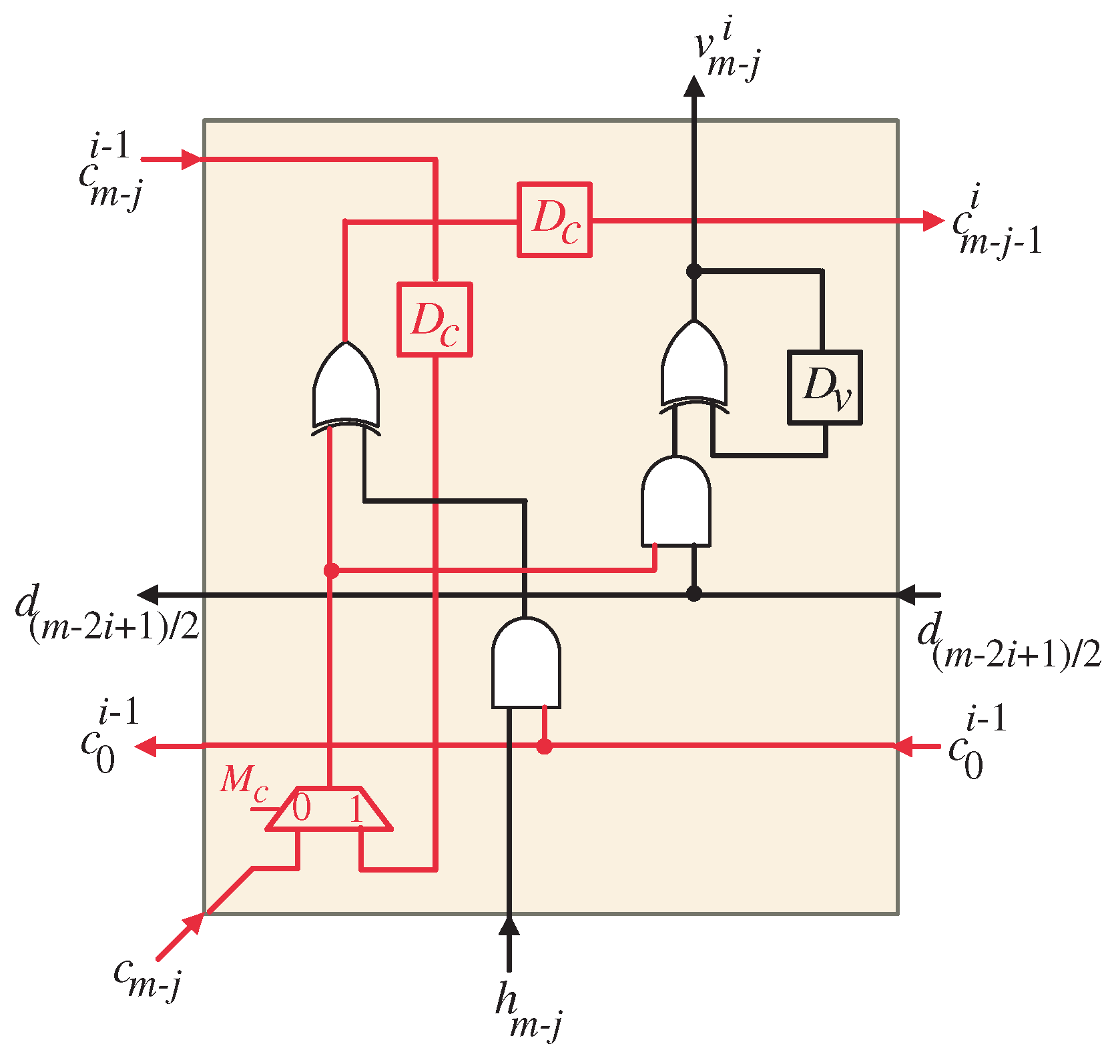
4. Dependency Graph
The iterative portion of the Montgomery multiplication algorithm involves recursive Equations (3), (6), (8) and (11) that describe the computation steps. These equations have a similar computation structure but differ in terms of their coordinate directions. To better understand the computational dependencies and patterns in the algorithm, we can represent them using DGs. These DGs provide a visual representation of the computations involved in the iterative portion of the algorithm. In this case, we have derived DGs for a specific field size of
, which are displayed in
Figure 2 and
Figure 3. These graphs are defined in a two-dimensional integer domain
, with indices
i and
j indicating the nodes in the graph.
By analyzing the DGs, we can gain insights into the parallelism and coordination of the computations in the algorithm. Each node in the DG represents a computation step, and the edges between nodes indicate the dependencies between these steps. The iterative formulas of the algorithm are computed by these nodes, which can be organized and scheduled to exploit parallelism and optimize performance.
The DGs provide valuable information for designing efficient hardware architectures for the Montgomery multiplication algorithm. By understanding the dependencies and patterns in the iterative computations, it is possible to develop specialized structures that maximize parallelism, minimize resource usage, and optimize performance. These architectures can be particularly beneficial in the context of VLSI implementation, where efficient hardware utilization is crucial.
In
Figure 2, the data entry points within the DG are organized along designated pathways to facilitate an orderly processing sequence. The following section outlines the various input pathways along with their associated signals:
Left-to-Right pathway: This pathway serves to introduce the input signals , with . These signals are fed into the DG from the left edge, ensuring a smooth integration into the processing sequence. The notation indicates the specific indexing of the input signals based on the field size m.
Top Entry Point: The top portion of the DG serves as the entry point for the input signals and the initial zero values of signals , where .
Red Slanted Lines: The reddish angled lines at the rightmost spots of the entry points are for the insertion of the input signals , where .
Inside DG, each node computes the intermediate outputs of the coefficients associated with the variable U. Once calculated, these outputs are transmitted to the nodes located in the subsequent row, adhering to the pathways indicated by the arrows in the graph. This procedure persists until the final row of the DG is attained. At the bottom of the DG, the resulting coefficients of variable U are produced. These coefficients represent the final output of the computation process. By organizing the inputs and computations in this manner, the DG facilitates the calculation of intermediate partial products and the generation of the final output coefficients of variable U. The directional flow ensures that the computations are performed in the desired order and that the dependencies between the nodes are properly maintained.
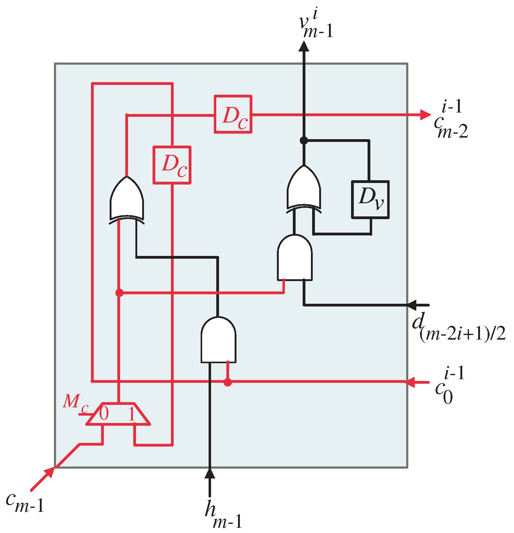
In a similar fashion, the data entering the DG depicted in
Figure 3 are strategically organized along specific pathways to enable the necessary calculations to occur. Let us take a closer look at these input paths and the various types of signals they convey:
Right-to-Left pathway: The pathway moving from right to left serves to introduce the input signal , where i is constrained to be between 1 and . These data points are fed into the DG from the lateral right edge.
Bottom Entry Point: The lower section of the DG serves as the designated area for inserting the input signal alongside the starting values of zero for the signal . This insertion takes place for indices satisfying the condition .
Red Slanted Lines: The red slanted lines depicted at the left corners of the input nodes are used to insert the input signals , where .
Within the DG, each node calculates the cumulative totals of the V data coefficients. These totals are then passed on to the nodes in the next row, following the paths indicated by the arrows in the diagram. This ensures that each node builds upon the information received from the previous row. This iterative process continues until the uppermost row of the DG is attained, providing a comprehensive overview of the data. At the top of the DG, the resulting coefficients of variable V are produced. These coefficients represent the final output of the computational process.
The final product T is obtained by summing the resulting coefficients of and . To implement this summation, 2-input XOR gates can be utilized. Each corresponding bit of the coefficients is connected to an input of the XOR gate. The outputs of the XOR gates are then combined to obtain the final result T.


