1. Introduction
After the invention of the first microphone in 1876, carbon microphones were introduced in 1878 as key components of early telephone systems. In 1942, ribbon microphones were developed for radio broadcasting. The invention of the self-biased condenser or electret microphones (ECM) in 1962 represented the first significant breakthrough in this field. Indeed, ECMs, ensuring high-sensitivity and wide bandwidth at low cost, have dominated the market for high-volume applications until the last decade, when MEMS microphones started to gain popularity [
1].
The first microphone based on silicon micro-machining (MEMS microphone) was introduced in 1983. Thanks to the use of advanced fabrication technologies, MEMS microphones offer several advantages with respect to ECMs: better performance, smaller size, compatibility with high-temperature automated printed circuit board (PCB) mounting processes, and lower sensitivity to mechanical shocks. Moreover, MEMS microphones can be integrated together with the CMOS electronics on the same chip or, more commonly, within the same package [
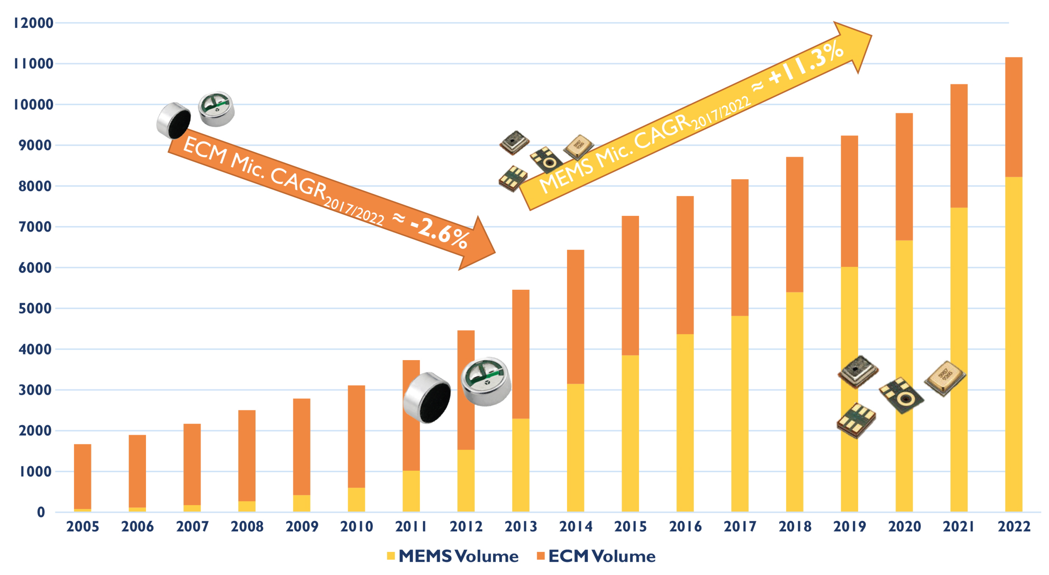
2], thus reducing area, complexity, and costs, while increasing efficiency, reliability, and performance. As a result, around 2014 MEMS microphones overcame ECMs in terms of sold units, with an annual market size increase of more than 11%, as shown in
Figure 1.
MEMS microphones can be realized exploiting different transduction principles, such as piezoresistive, and optical detection. However, more than 80% of the produced MEMS microphones are based on capacitive transduction, since it achieves higher sensitivity, consumes lower power, and is more compatible with batch production. Piezoelectric MEMS microphones are also gaining popularity as an alternative to capacitive devices, since they do not require a biasing voltage, but so far they have not reached the same level of performance and cost effectiveness.
The interface circuit is of paramount importance for MEMS microphones, since it represents one of the most significant competitive advantages with respect to ECMs. Therefore, the development of high-performance interface circuits has been proceeding in parallel with the evolution of MEMS microphones since the very beginning [
4,
5,
6,
7,
8,
9,
10,
11,
12]. The main target in the optimization of these interface circuits is the constant improvement of the audio performances, such as signal-to-noise ratio (
), dynamic range (
), and total harmonic distortion (
), while maintaining or even reducing the power consumption. This trend is mainly driven by portable applications, in which the audio-related functionalities have been expanding significantly. For example, voice interfaces are becoming pervasive. A growing number of people now talk to their mobile devices, asking them to send e-mails and text messages, to search for directions, or to find information on the internet. These functions require continuous listening, thus introducing severe constraints on the power consumption of the microphone modules. On the other hand, mobile devices nowadays are also used to perform high-fidelity (Hi-Fi) audio/video recording, which require high performance in terms of
and
. Such different scenarios are clearly characterized by different performance and power consumption requirements in the microphone module. Different operating modes are required when the same device is re-used in different systems (with different specifications) or when, in the same system, the specifications change depending on the performed function.
In the first case, applications with different
requirements lead to different component choices, like, for instance, different microphones and/or audio processors. In this situation, the microphone interface circuit has to achieve different performance levels depending on the hardware to which it is connected. In the second case, portable devices supporting voice commands require the audio module to be always active, featuring low
with low power consumption in stand-by mode (to extend battery life) [
13]. However, as soon as an audio input signal is detected, the
and, hence, the power consumption of the audio module have to be increased to effectively perform the required functions. Then, as soon as the input signal vanishes, the system has to return in stand-by mode. For instance, in always running applications, the bandwidth and
requirements are typically relaxed (e.g., 4-kHz bandwidth and
dB), but power consumption has to be extremely low [
14,
15,
16], whereas, in Hi-Fi applications, the required bandwidth is 20 kHz and the
has to be larger than 90–100 dB, but a relatively high (e.g., around 1 mW) power consumption can be tolerated [
17,
18,
19,
20,
21,
22,
23,
24].
As a consequence, in the last decade, MEMS microphone interface circuits evolved from just simple amplification stages to complex mixed-signal circuits, including A/D converters, with ever increasing performance.
This paper is organized as follows.
Section 2 provides a short overview of MEMS microphones, briefly describing their operating principle. Then,
Section 3 discusses the basic principles of the interface circuits for MEMS microphones, illustrating the most important design options and trade-offs, as well as the evolution of both the architecture and the performance over the last decade. This evolution is then analyzed in detail with four actual design examples, which are described in
Section 4,
Section 5,
Section 6 and
Section 7, respectively. Finally, in
Section 8, we draw some conclusions and discuss future trends.
2. Capacitive MEMS Microphones
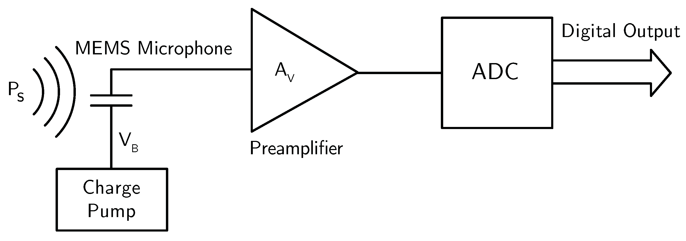
A microphone is a transducer, which translates a perturbation of the atmospheric pressure, i.e., sound, into an electrical quantity. In a capacitive MEMS microphone, the pressure variation leads to the vibration of a mechanical mass, which, in turn, is transformed into a capacitance variation.
Sound pressure is typically expressed in (sound-pressure-level). A sound pressure of 20 Pa, corresponding to 0 , is the auditory threshold (the lowest amplitude of a 1-kHz signal that a human ear can detect). The sound pressure level of a face-to-face conversation ranges between 60 and 70 . The sound pressure rises to 94 if the speaker is at a distance of one inch from the listener (or the microphone), which is the case, for example, in mobile phones. Therefore, a sound pressure level of 94 , which corresponds to 1 Pa, is used as a reference for acoustic applications. The performance parameters for acoustic systems, such as , are typically specified at 1-Pa and 1-kHz.
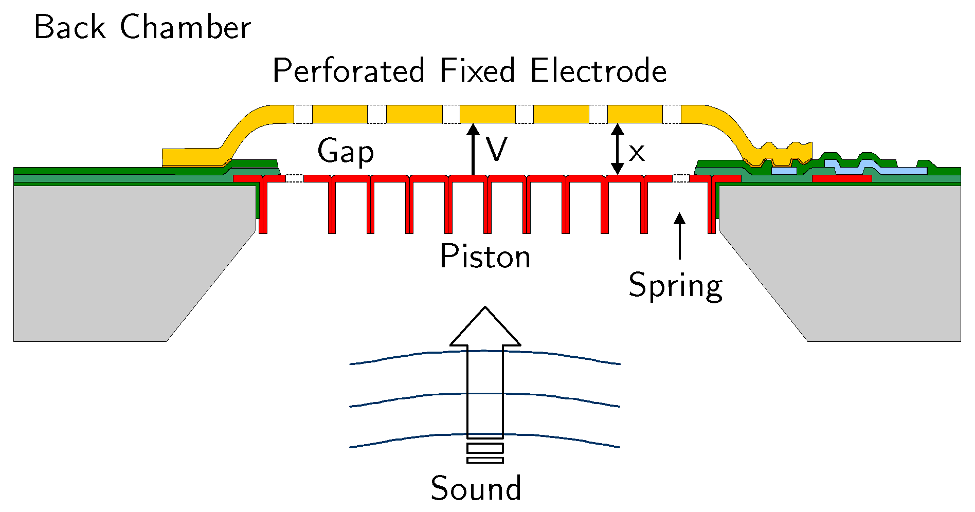
A MEMS microphone, whose simplified structure is shown in
Figure 2, consists of two conductive plates at a distance
x. The top plate, in this case, is fixed and cannot move, while the bottom plate is able to vibrate with the sound pressure, producing a variation of
x (
) with respect to its steady-state value (
), proportional to the instantaneous pressure level (
). Different arrangements of the electrodes and fabrication solutions are possible [
25,
26,
27,
28,
29,
30,
31], but the basic principle does not change.
The capacitance of a MEMS microphone can then be written as
where
A is the area of the smallest capacitor plate and
is the vacuum dielectric permittivity.
Denoting with
the MEMS capacitance in the absence of sound, i.e., when
, and assuming linear the relationship between the sound pressure
and the deformation
x (
), which is actually true for
, we can calculate the output signal (
) as a function of
. If the MEMS capacitor is initially charged to a fixed voltage
, the charge
remains constant, independently of
. As a consequence, the capacitance variation due to a sound pressure variation
leads to a voltage signal (
) given by
where
denotes the voltage sensitivity of the microphone.
According to (
2),
depends on the bias voltage
. Therefore, in order to increase the microphone sensitivity and, hence, the
, the value of
has to be pretty high, typically ranging from 5 V to about 15 V. As a consequence, a charge pump is usually required to generate the desired value of
, starting from the standard CMOS power supply voltage (1.8 V, 2.5 V, or 3.3 V).
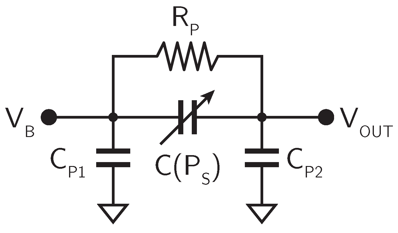
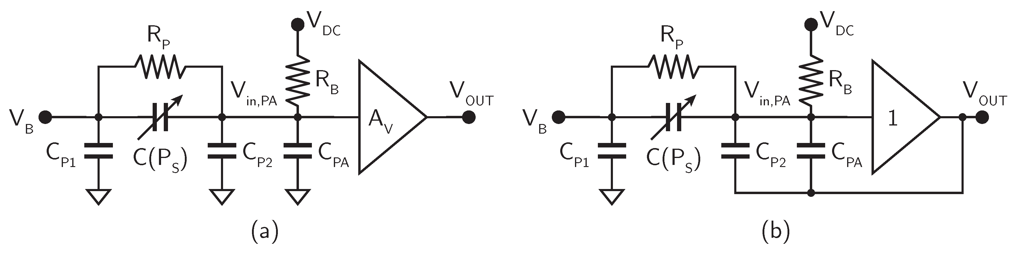
In practical implementations, a MEMS microphone is not just a capacitor, but some additional parasitic components have to be taken into account. The equivalent circuit of an actual MEMS microphone is shown in
Figure 3.
Besides the variable capacitance , the equivalent circuit includes two parasitic capacitances and , connected between each plate of the MEMS microphone and the substrate, as well as a parasitic resistance , connected in parallel to . The value of these parasitic components depends on the specific implementation of the microphone, but typically and are of the order of few pF, while is in the G range.
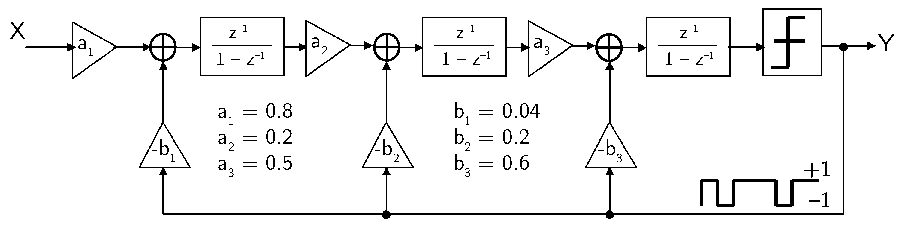
4. Example 1: Third-Order DT Modulator
As a first design example, we consider a DT
modulator used in one of the very first MEMS microphone interface circuits [
7,
41]. In this interface circuit, considering the sampling frequency
MHz and, hence, the oversampling ratio
, according to Equation (
5), a third-order (
), single-bit (
)
modulator is sufficient to achieve the required
dB. The block diagram of the third-order DT
modulator is shown in
Figure 7.
The signal transfer function (
) and the noise transfer function (
) are given by
respectively.
Figure 8 shows the switched-capacitor (SC) implementation of the
modulator.
The feedforward and feedback paths are implemented using separate capacitors, thus relaxing the settling requirements of the operational amplifiers. The feedback path contains an extra switch, to select between positive and negative reference voltage ( or ). The first integrator has reduced output swing, but the capacitors are large to keep the noise low, while the second and third integrator use smaller capacitors, but the output swing is large. Therefore, all the integrators have almost the same settling requirements for the operational amplifiers. Bottom-plate sampling is used in the whole modulator to minimize the distortion due to charge-injection from switches.
The operational amplifiers used for the integrators are based on a telescopic-cascode topology. The common-mode feedback is realized with an SC network. The comparator used consists of a differential stage with regenerative load, followed by a set–reset flip-flop.
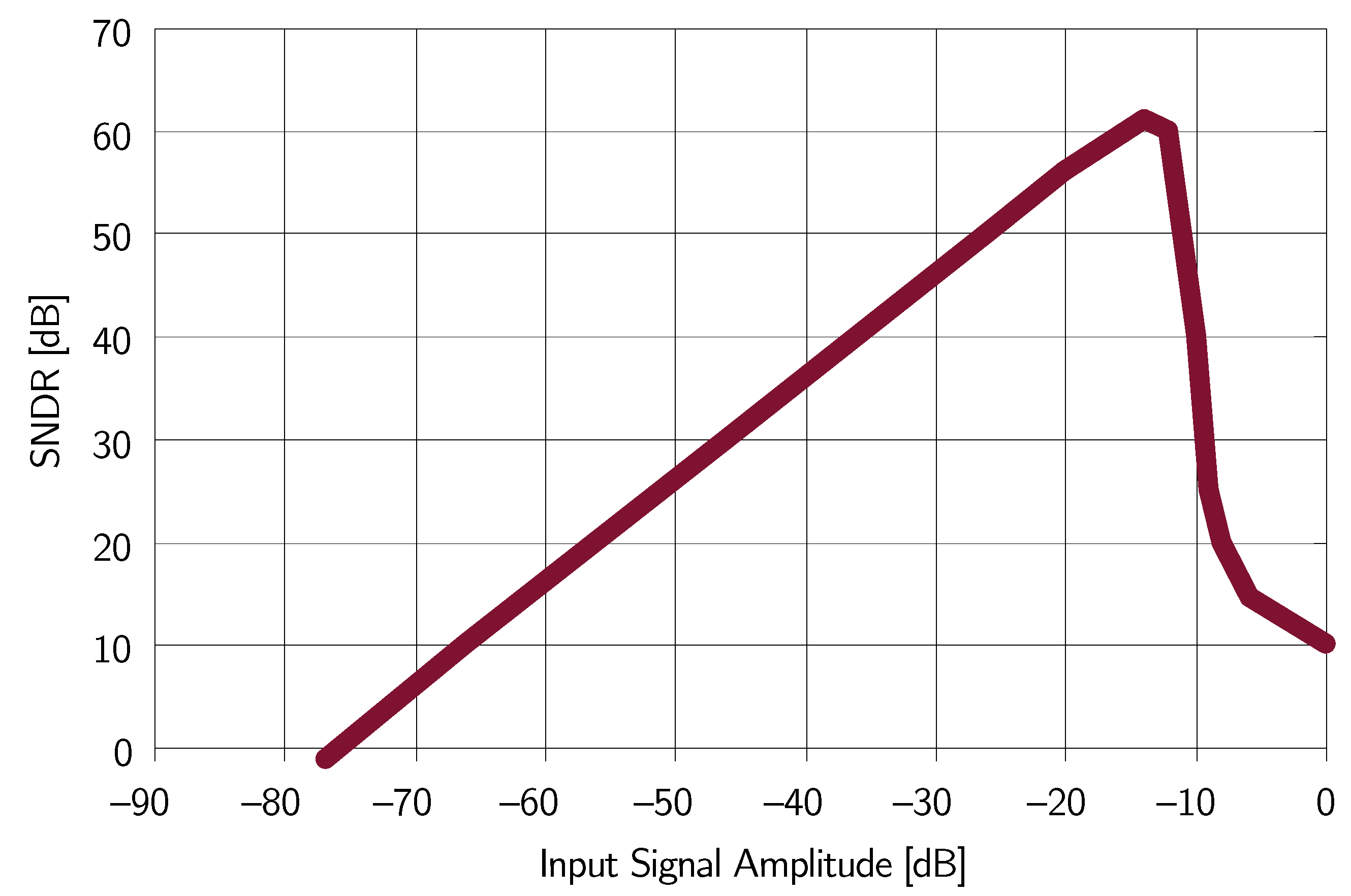
Experimental Results
The interface circuit has been fabricated using a 0.35-m CMOS technology with four metal and two polysilicon layers. The circuit consumes 210 A for the analog section and 90 A for the logic, respectively, leading to an overall power consumption of 1.0 mW with a sampling frequency of 2.52 MHz and a power supply voltage of 3.3 V. The chip area is 3.15 (1930 m × 1630 m), including pads.
Figure 9 shows the achieved
as a function of the input signal amplitude with an input signal frequency of 1 kHz. The peak
equal to 61 dB is achieved with an input signal amplitude of
, corresponding to a sound pressure of 104
for the considered MEMS microphone. By considering both noise and distortion contributions, the achieved
is equal to 9.8. The achieved
is 76 dB.
Finally,
Table 1 summarizes the most important measured performances.
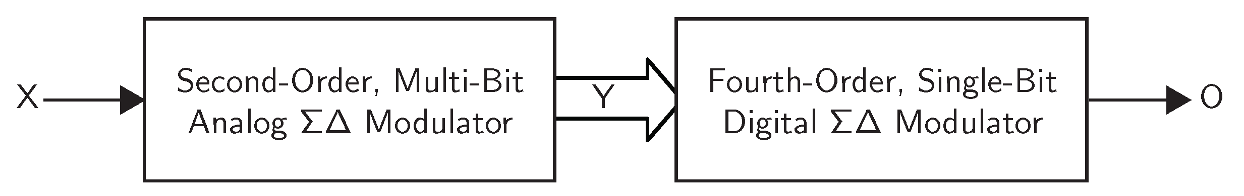
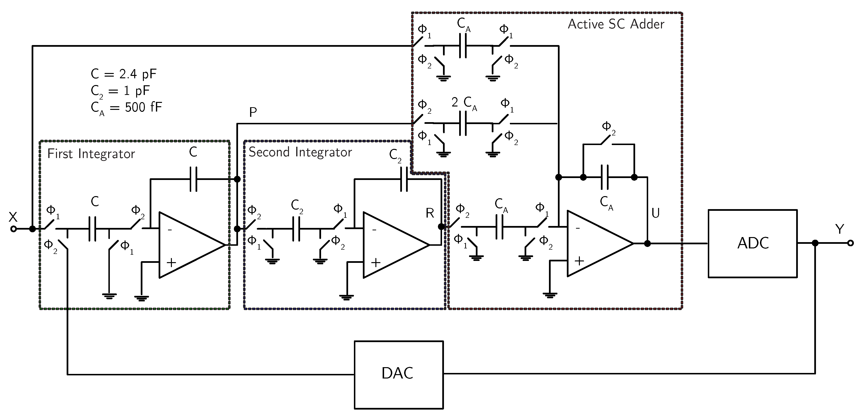
5. Example 2: Second-Order Multi-Bit DT Modulator
The second design example is a MEMS microphone interface circuit again based on DT
modulator [
12]. Considering a sampling frequency
MHz, with a signal bandwidth
kHz, and hence an oversampling ratio
, according to (
5), the required
dB and a single-bit output stream can be achieved, for example, with a single-bit quantizer (
) and a fourth-order noise shaping (
). However, this solution suffers from instability for large input signals, thus requiring watch-dog circuits in order to guarantee saturation recovery. Moreover, at least four operational amplifiers have to be used to design the loop filter.
Another possible solution is to use a 2-2 multi-stage noise shaping (MASH)
modulator [
33,
34] to achieve the required
, while overcoming instability issues. However, this solution does not provide a single-bit output stream because of the additional digital filter required to combine the outputs of the cascaded modulators, and suffers from quantization noise leakage problems, due to mismatches between the analog integrators and the digital filter. Moreover, it still requires four operational amplifiers.
According to (
5), the required
is also obtained with
and
(e.g., 12-level quantizer). This solution can be easily designed to be stable even for a large input signal and requires only two operational amplifiers to implement the loop filter. Moreover, multi-bit feedback alleviates the slew-rate requirements of the operational amplifiers. However, this solution does not provide fourth-order noise shaping nor single-bit output stream. These drawbacks can be solved by connecting at the output of the multi-bit, second-order, analog
modulator a single-bit, fourth-order, digital
modulator, operated at the same sampling frequency
, which truncates the multi-bit output down to a single bit and shapes the resulting truncation error with a fourth-order transfer function. The digital, fourth-order
modulator is less critical than its analog counterpart, since it can be easily verified under any operating conditions, and, by using sufficiently large word-length in the integrators and a suitable noise transfer function, instability can be avoided. This solution, whose block diagram is shown in
Figure 10, is very promising to achieve the specifications of power consumption and resolution of the system. In order to verify the achievable performance with the used
modulator architecture and derive the specifications for the building blocks, behavioral simulations, including most of the non-idealities (
noise, jitter, operational amplifier noise, gain, bandwidth and slew rate), have been performed using a dedicated toolbox [
35]. The achieved
is 82.4 dB, which corresponds to an effective number of bits (
) of 13.4.
Several solutions are available in literature to obtain a DT analog second-order
modulator [
39]. Among them, the second-order
modulator architecture, whose block diagram is shown in
Figure 11 [
42], is particularly suited for the considered application, since, thanks to the feedforward paths from the input of the integrators to the input of the quantizer, the output of the integrators consists of quantization noise only, thus allowing low-performance (and hence low-power) operational amplifiers to be used.
The analog
modulator consists of two integrators, one adder, a flash ADC, and a multi-bit digital-to-analog converter (DAC). The circuit features
, and
with second-order noise shaping. Both the integrator outputs consist of quantization noise only, whose maximum amplitude is equal to
, where
is the reference voltage (i.e., the full scale value) and
is the number of levels in the quantizer.
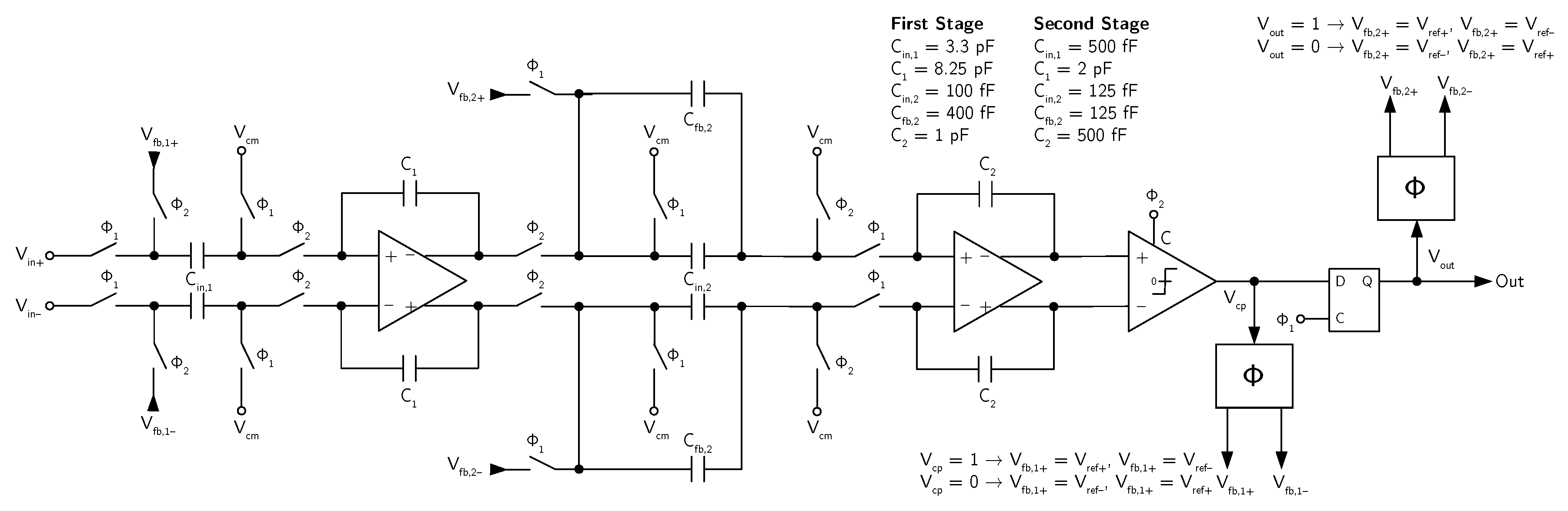
Figure 12 shows the SC implementation of the DT analog second-order
modulator. The circuit is actually fully-differential, although, for simplicity,
Figure 12 shows a single-ended version. An active block has been used to implement the adder before the quantizer, in order to reduce the capacitive load for the two integrators, thus reducing the power consumption. This solution requires an additional operational amplifier but, thanks to the reduced capacitive load, it consumes less power anyway than a solution based on a passive adder.
The operational amplifiers used for the integrators and the adder are based on a folded-cascode topology. The common-mode feedback is realized with an SC network.
The quantizer (flash ADC) consists of comparators, thus leading to a 12-level output code. The comparator used in the flash ADC consists of a pre-amplifier followed by a clock-driven regenerative latch. The fully-differential comparison between the input signals and the threshold voltages is performed before the pre-amplification stage by an SC network.
The DAC is realized by splitting the input capacitance C of the first integrator into 12 identical parts, which are alternately connected to , or , according to the quantizer output.
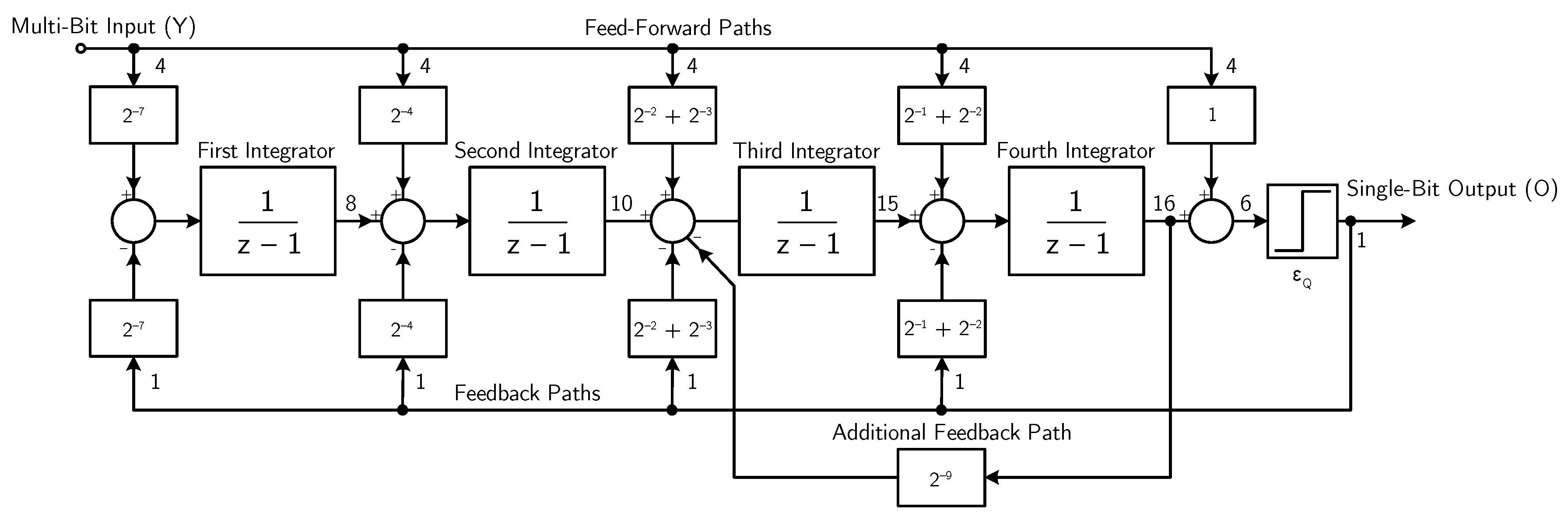
The block diagram of the DT digital fourth-order, single-bit
modulator is shown in
Figure 13. Denoting with
Y and
the modulator input and the quantization noise, respectively, the modulator output signal
O is given by
thus leading to a unitary
in the audio band and an
with fourth-order noise shaping. The coefficients of the
modulator are implemented as the sum of no more than two terms, each expressed as a power of 2, thus avoiding the use of multipliers.
The word-length in the internal registers is 8 bits for the first integrator, 10 bits for the second integrator, 15 bits for the third integrator, 16 bits for the fourth integrator, and 6 bits for the final adder, in order to avoid saturation and truncation, under any operating conditions.
Experimental Results
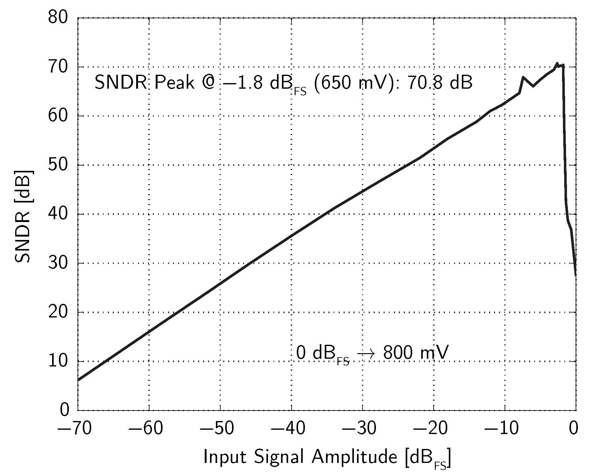
The interface circuit has been fabricated using a 0.35-m CMOS technology with four metal and two polysilicon layers. The circuit consumes 215 A for the analog section and 95 A for the digital section, respectively, leading to an overall power consumption of 1.0 mW with a clock frequency of 2.048 MHz and a power supply voltage of 3.3 V. The chip area is 3 (1755 m × 1705 m), including pads. The full-scale input signal amplitude is equal to the DAC reference voltage (), which has been set to mV, i.e., mV peak-to-peak, which, for the considered MEMS microphone, corresponds to about 106 .
Figure 14 shows the achieved
as a function of the input signal amplitude with an input signal frequency of 1 kHz. The peak
is equal to 71 dB. By considering both noise and distortion contributions, the achieved
is equal to 11.5. The achieved
is 77 dB. The use of a feedforward path in the analog, second-order
modulator allows the peak
to be achieved for an input signal amplitude as large as
.
Finally,
Table 2 summarizes the most important measured performances.
6. Example 3: Fourth-Order MASH DT Modulator
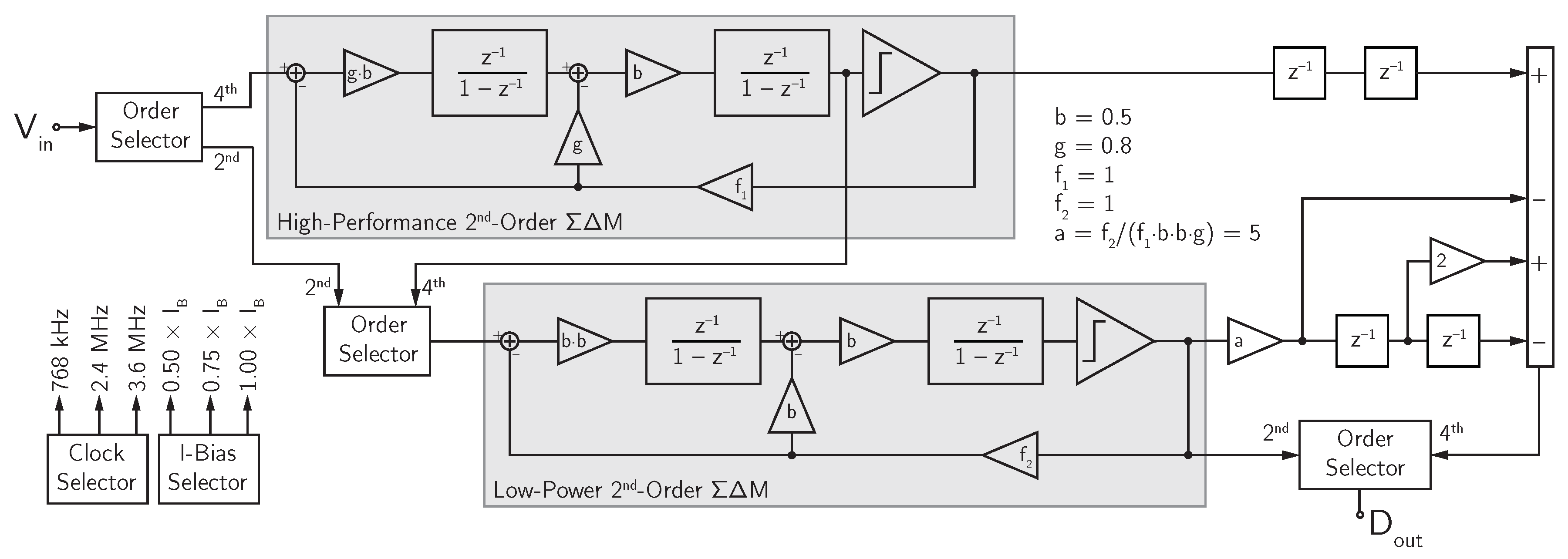
The third design example belongs to the new generation of MEMS microphone interface circuits. This interface circuit is based on a reconfigurable MASH 2-2 DT
modulator, which can efficiently target different functions and/or applications, as discussed in
Section 1 [
22,
24]. The reconfigurable DT
modulator can operate in different modes depending on the target function or application. In particular, it is possible to select the
modulatror order (second or fourth), the sampling frequency (768 kHz, 2.4 MHz, or 3.6 MHz), the signal bandwidth (4 kHz or 20 kHz), and the bias current level (50%, 75%, or 100% of the nominal value). Among the several resulting operating modes, the three most common ones are:
Low-Power (LP) mode (second order, kHz, 4-kHz bandwidth, 50% bias current level);
Standard (ST) mode (fourth order, MHz, 20-kHz bandwidth, 75% bias current level);
High-Resolution (HR) mode (fourth order, MHz, 20-kHz bandwidth, 100% bias current level).
The block diagram of the
modulator is shown in
Figure 15. It consists of two cascaded second-order stages and a digital recombination filter. The MASH topology has been selected for several reasons. Firstly, it can be made unconditionally stable for input signals bounded within the full-scale, value independently of the operating mode. Moreover, in the presence of accidental signal overload beyond the full-scale value, it guarantees fast recovery. The inherent stability feature allows the
to be maintained close to the ideal value given by Equation (
5).
With three selectors, it is possible to reconfigure the modulator in a fourth-order or in a second-order topology. When the fourth-order topology is selected, both stages are active, the input is applied to the first stage, the output of the second integrator of the first stage is fed into the second stage, and the multi-bit output is read after the digital recombination network, which merges the bitstreams produced by the two stages. On the other hand, when the second-order topology is selected, only the second stage is active (while the first stage is turned-off), and the input is applied directly to the second stage from which the single-bit output is read.
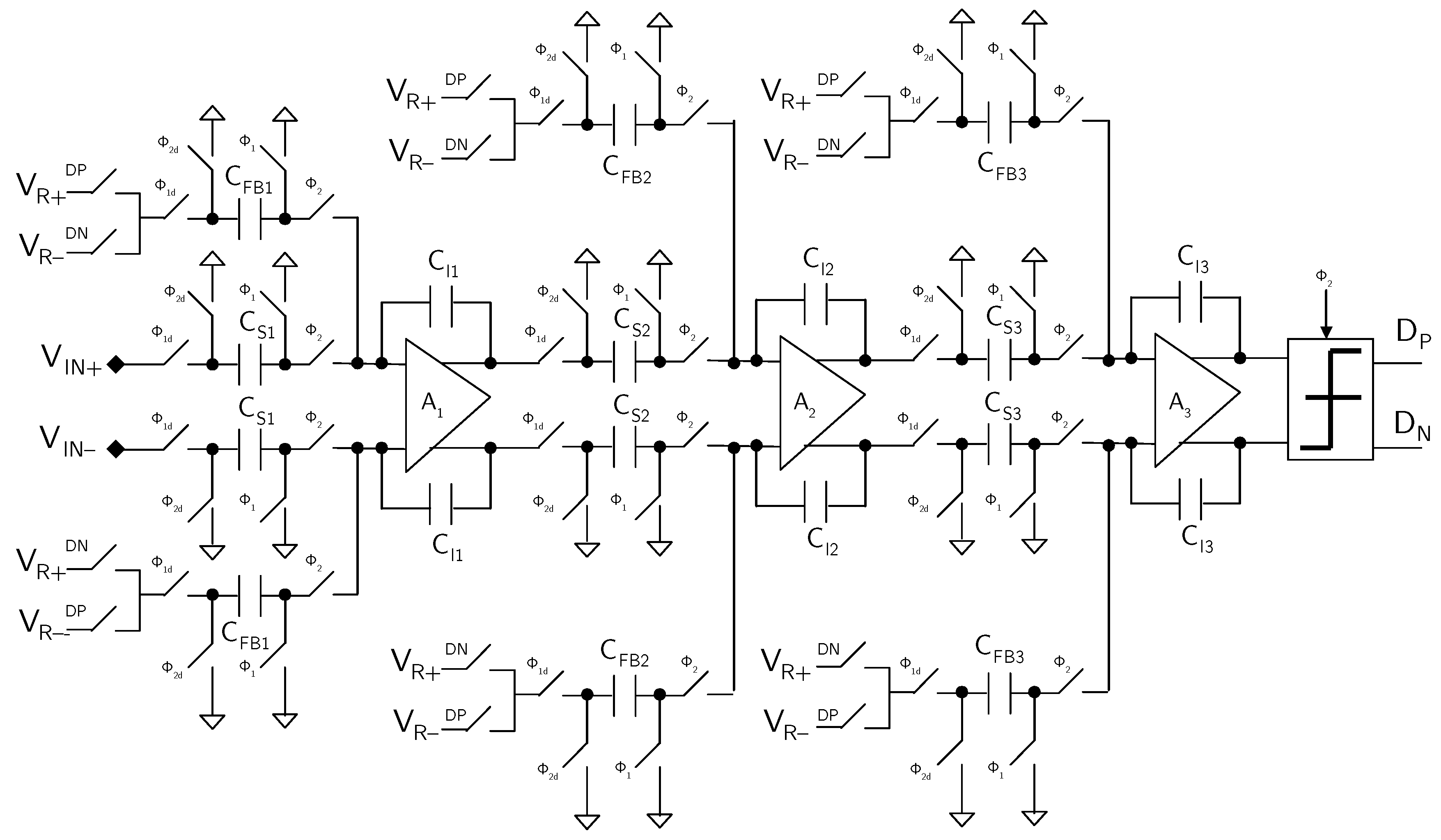
The first and the second stages of the DT MASH
modulator structure are topologically identical. The fully-differential SC implementation of each second-order stage is shown in
Figure 16.
In each second-order modulator stage of the MASH structure, the coefficients are optimized to ensure that the integrator output swing remains within the allowed range under any operating conditions. The coefficients of the digital recombination filter have, then, been set accordingly, in order to properly cancel the first-stage quantization noise from the global modulator output in the operating modes featuring fourth-order noise shaping.
The noise requirements of the second stage are relaxed with respect to the first stage both with fourth-order noise shaping (when the second-stage requirements are reduced by the first-stage gain) and with second-order noise shaping (when lower target specification are required). The softened noise requirements for the second stage are exploited for reducing the capacitance values and the bias current with respect to the first stage. In the same way, inside each stage, the second integrator is designed with lower noise performance (i.e., lower capacitance values and lower bias current) with respect to the first integrator.
Experimental Results
The reconfigurable MASH SC modulator has been fabricated in a 0.18-m CMOS process. The chip area is , including the modulator, the reference buffers, and an LDO regulator to stabilize the power supply voltage. The reference voltages and are mV around the common mode voltage mV (i. e. the modulator full-scale input signal is 2 ). These reference voltages are constant independently of the operating mode (they are actually produced by a bandgap reference circuit shared with other blocks in the complete audio module).
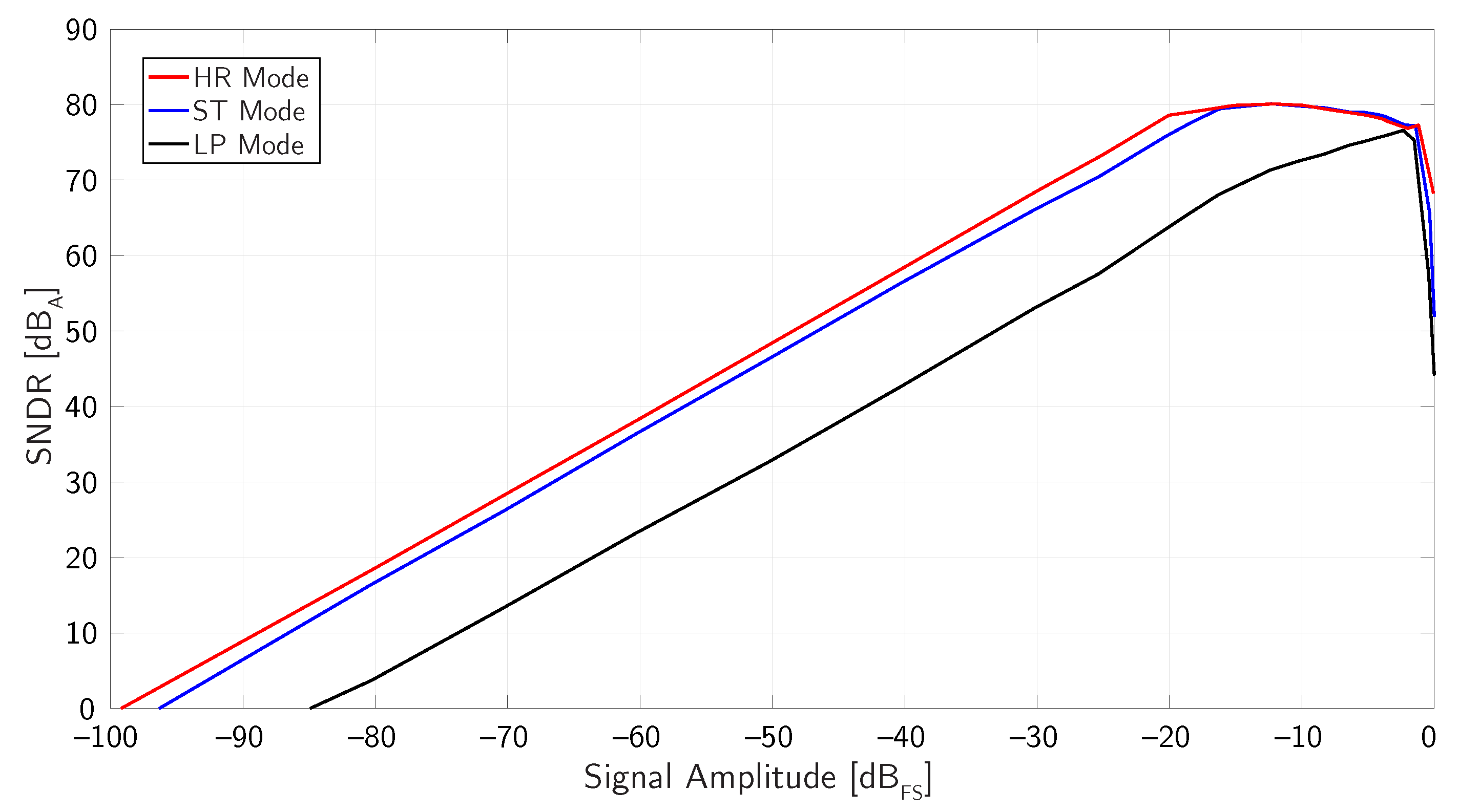
Figure 17 shows the measured
of the
modulator as a function of the input signal amplitude at 1 kHz in the three main modes of operation (HR, ST, and LP).
The circuit achieves a of 99 dB in HR mode, 96 dB in ST mode, and 85 dB in LP mode. The peak is limited in all operating modes to about 80 dB by the harmonic distortion of the signal source available for the measurements (in the considered application, the for sound pressures larger than 100 is anyway limited to about 75 dB by the harmonic distortion of the microphone).
The achieved
and power consumption of the reconfigurable
modulator for all the available operating modes are reported in
Table 3, demonstrating the flexibility of the device.
Finally,
Table 4 summarizes the the most important measured performances.
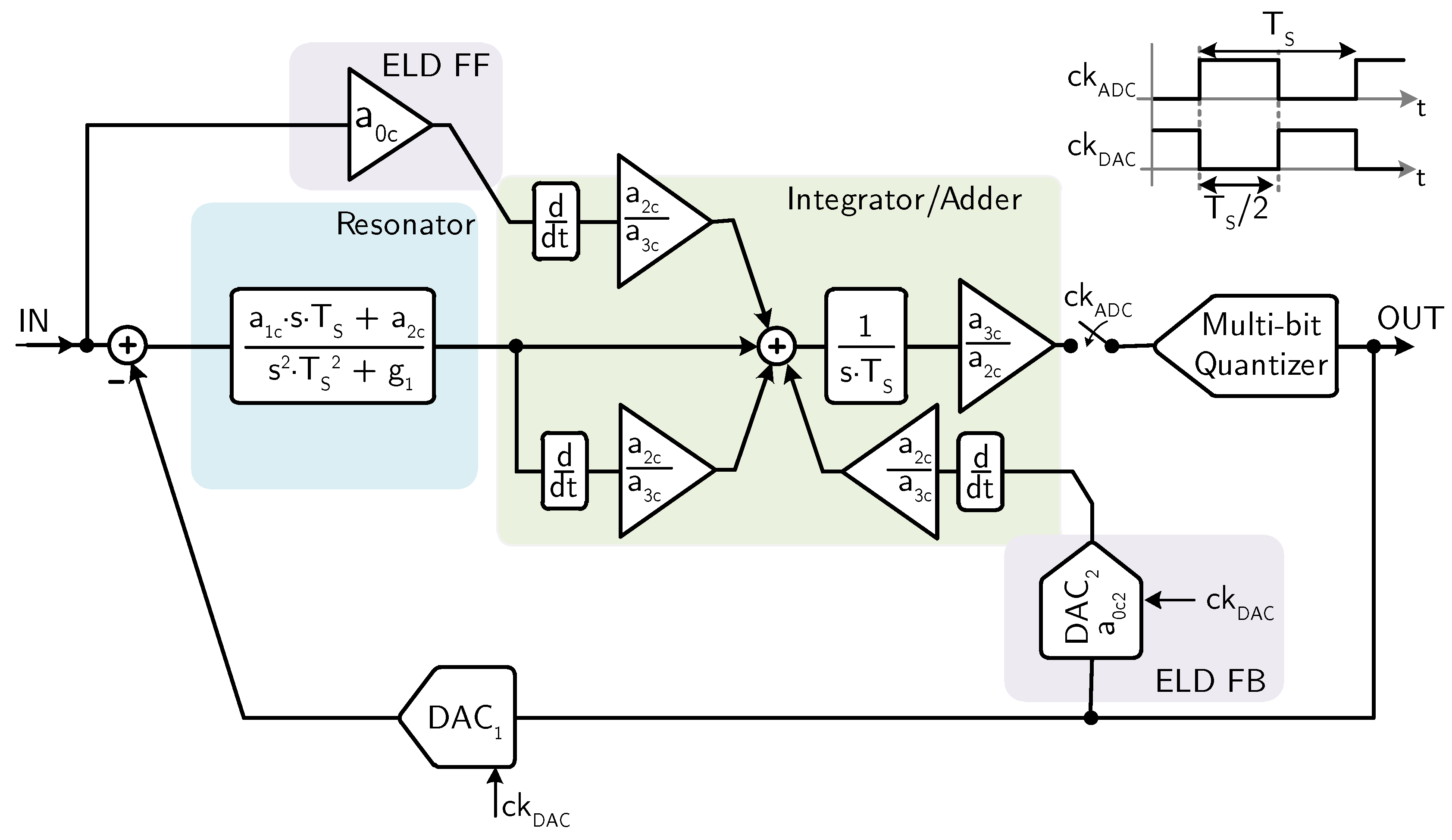
7. Example 4: Third-Order CT Modulator
The last example, one of the top-of-class interface circuits for MEMS microphones, is based on a third-order, multi-bit CT
modulator [
23]. The block diagram of the
modulator is illustrated in
Figure 18.
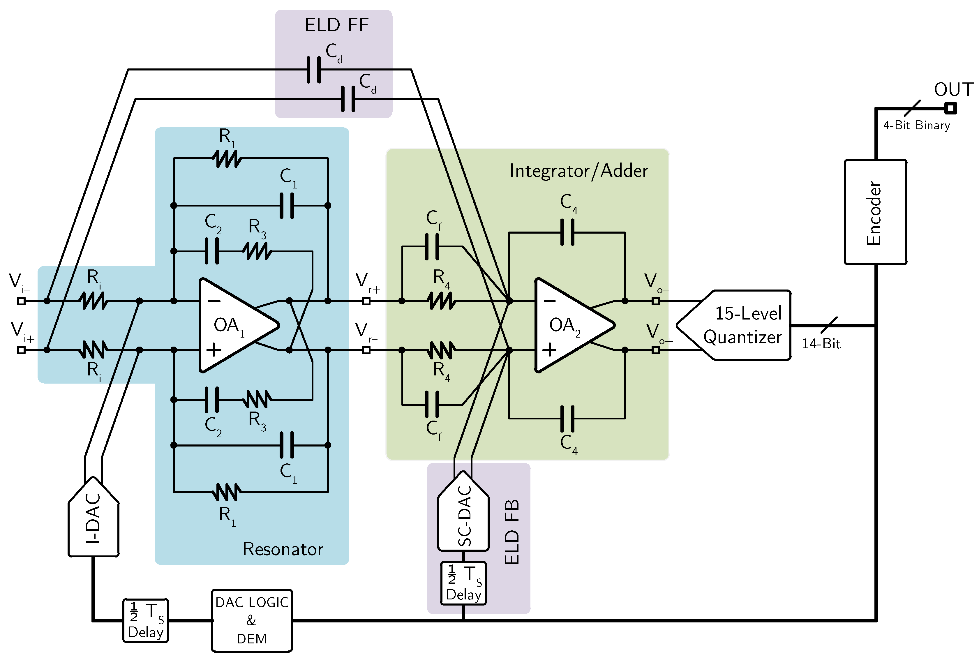
The loop filter consists of a resonator (second-order transfer function) followed by an integrator. A local feedback DAC around the quantizer () and a dedicated feedforward path are used for compensating the excess loop delay (ELD). The feedforward paths of the loop filter and the local ELD feedback are differentiated and added at the input of the integrator, in order to avoid an active adder at the input of the quantizer. The multi-bit quantizer drives a 15-level DAC () with dynamic element matching (DEM) to close the main feedback loop of the CT modulator.
The schematic of the active-RC implementation of the CT
modulator is shown in
Figure 19.
The resonator is implemented using a single operational amplifier and no active adder is used at the input of the quantizer, thus requiring only two operational amplifiers for implementing the third-order loop-filter transfer function. The local feedback DAC for ELD compensation is implemented with an SC structure, whereas the main feedback DAC is realized with a three-level (, 0, ) current-steering topology, which guarantees minimum noise for small input signals. Indeed, with the three-level topology, the unused DAC current sources are not connected to the resonator input and, hence, they do not contribute to the CT modulator noise. The multi-bit quantizer is realized with 14 identical differential comparators and a resistive divider from the analog power supply for generating the threshold voltages.
The values of the passive components used for implementing the CT
modulator are summarized in
Table 5. The value of
has been chosen as low as 47 k
to fulfill the thermal noise requirements, while
,
,
,
,
,
, and
are obtained consequently to achieve the desired CT
modulator coefficients. Eventually, resistors
can be removed if the preamplifier is realized with a transconductor which provides directly an output current. Both operational amplifiers are realized with a two-stage, Miller compensated topology in which transistor size and bias current are sized to fulfill the noise requirements (the values in the second operational amplifier are scaled with respect to the first one, since its noise contribution is negligible).
Experimental Results
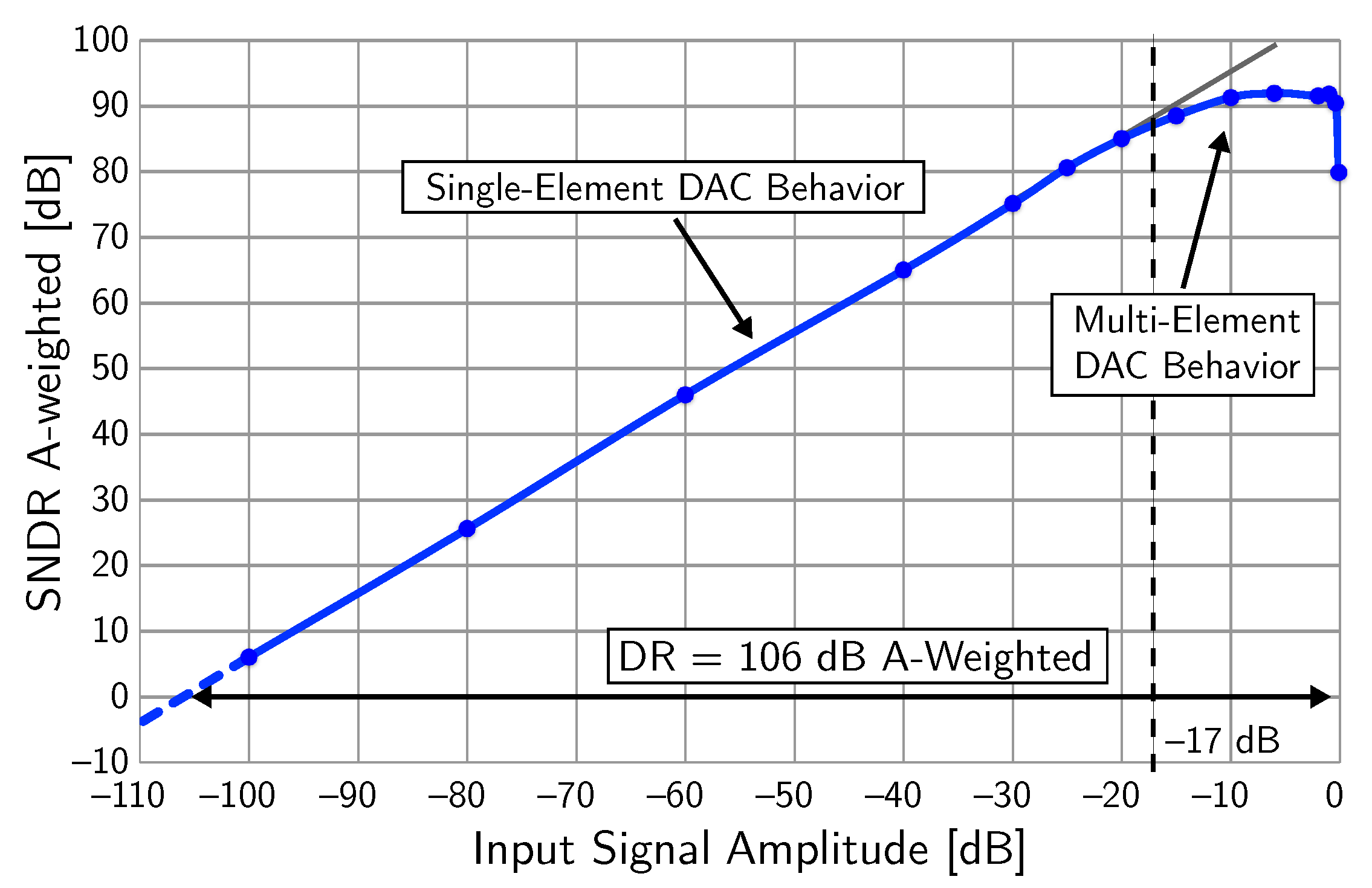
The third-order CT modulator has been fabricated using a 0.16-m CMOS technology. The chip area is 0.21-.
Figure 20 shows the measured
as a function of the input signal amplitude at 1 kHz. The full-scale input signal (0
) corresponds to 1
differential. The achieved
is 106 dB (A-weighted), corresponding to an
bits, whereas the peak
is 91.3 dB. The change of slope in the
curve for input signal amplitudes larger than
is due to the increased current-steering DAC noise when more than one three-level DAC element is used (acceptable for the microphone application, where the performance for large input signals is limited by the microphone itself).
The analog section of the third-order
modulator consumes 350
W, while the digital blocks (i.e., DEM and thermometer-to-binary converter) consume 40
W, both from a 1.6-V power supply and during conversion. The achieved value of
is 180 dB, which is among the highest reported for audio
modulators.
Table 6 summarizes the achieved performance.
8. Conclusions
Looking at the performance evolution in the four reported MEMS microphone interface circuit design examples, summarized in
Table 7, it appears clearly that in the last decade the trend has been in the direction of increasing the
and the
, while maintaining the power consumption in the hundreds of
W range, with the goal of reaching Hi-Fi audio quality (
dB) in portable devices, eventually introducing some reconfigurability to tackle scenarios, such as voice commands, where a power consumption lower than 100
W is required. This trend, obviously is reflected in a constant increase of
.
Further improvements of the audio quality beyond 110-dB are not desirable nor necessary, since the physical limitations in the microphone itself (such as Brownian noise) would anyway prevent the exploitation of such performance at system level. Therefore, the next goal in the development of MEMS microphone interface circuits is toward the reduction of the power consumption below 100 W, while maintaining the performance. Indeed, in this direction, there is still a lot of space for improvements, especially by exploiting the intrinsic features of the audio signals to dynamically adapt the power consumption. Voice activity detection, adaptive biasing, and tracking ADCs are some of the topics being investigated to achieve this target.


