Gimbal-Less Two-Axis Electromagnetic Microscanner with Twist Mechanism


Abstract
:1. Introduction
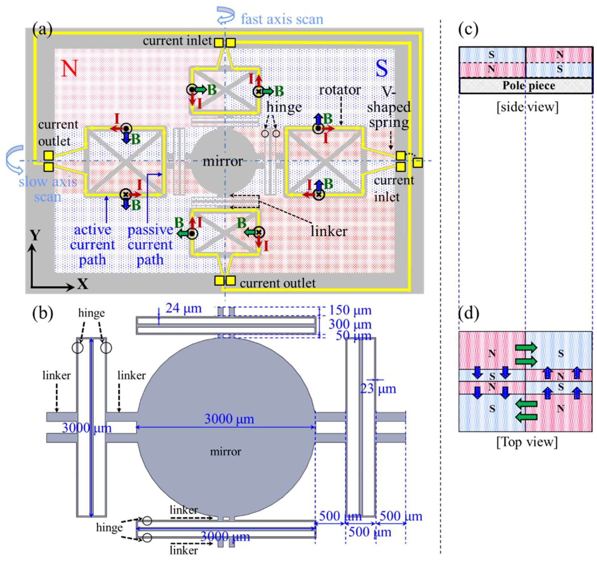
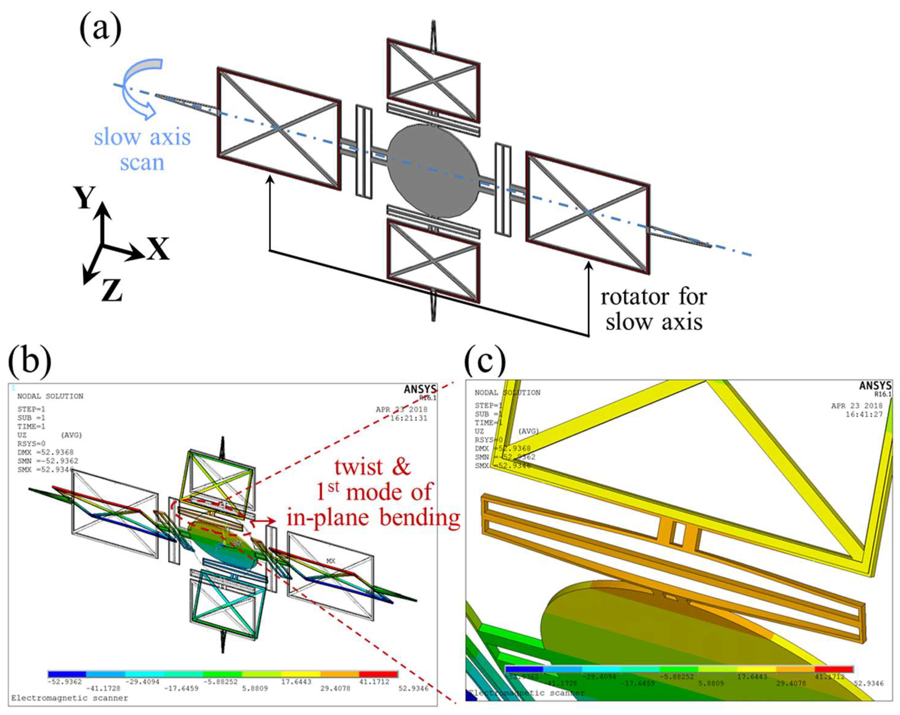
2. Design
2.1. Working Principle
2.2. Device Configuration
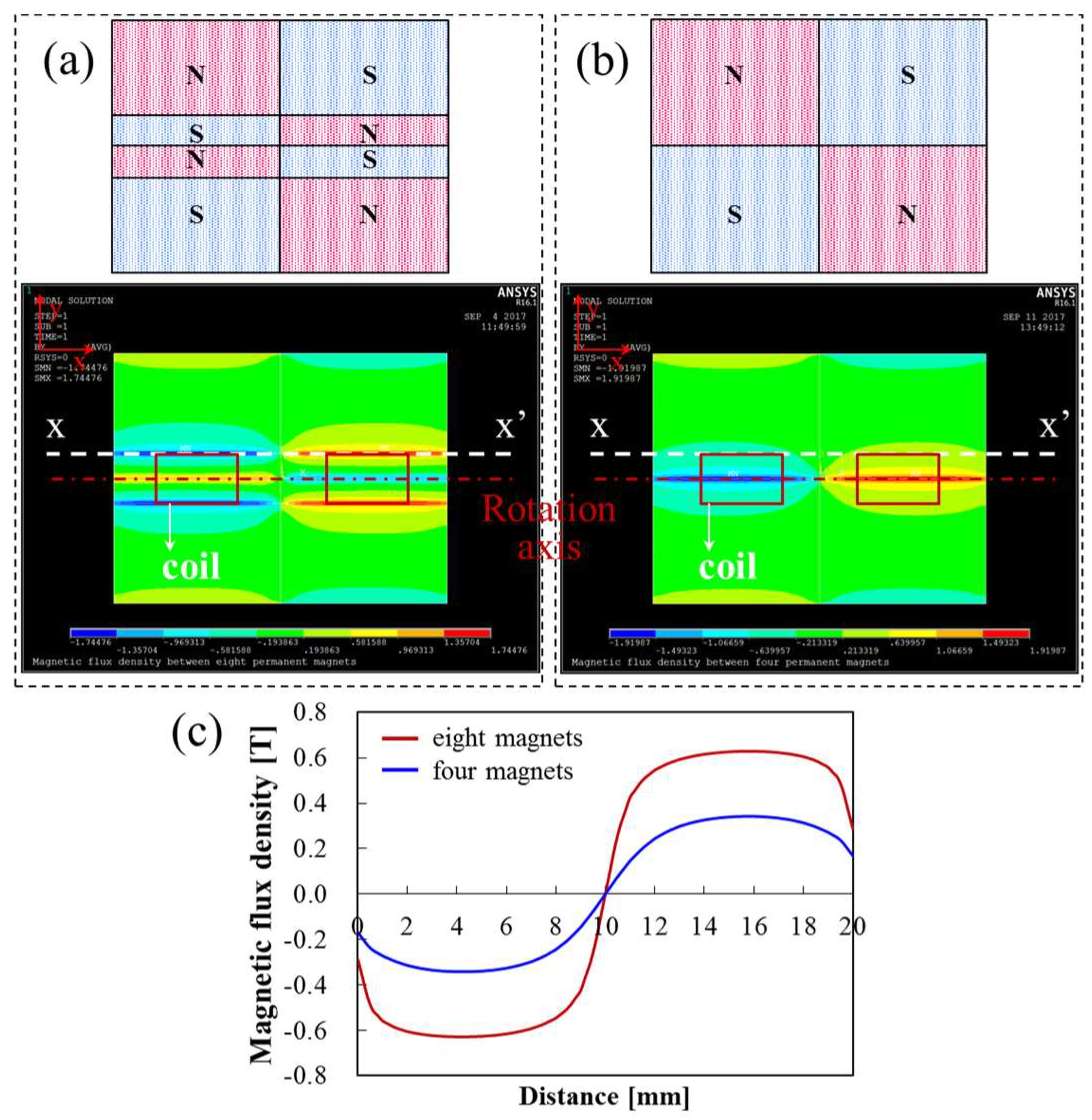
2.3. Magnetic Field
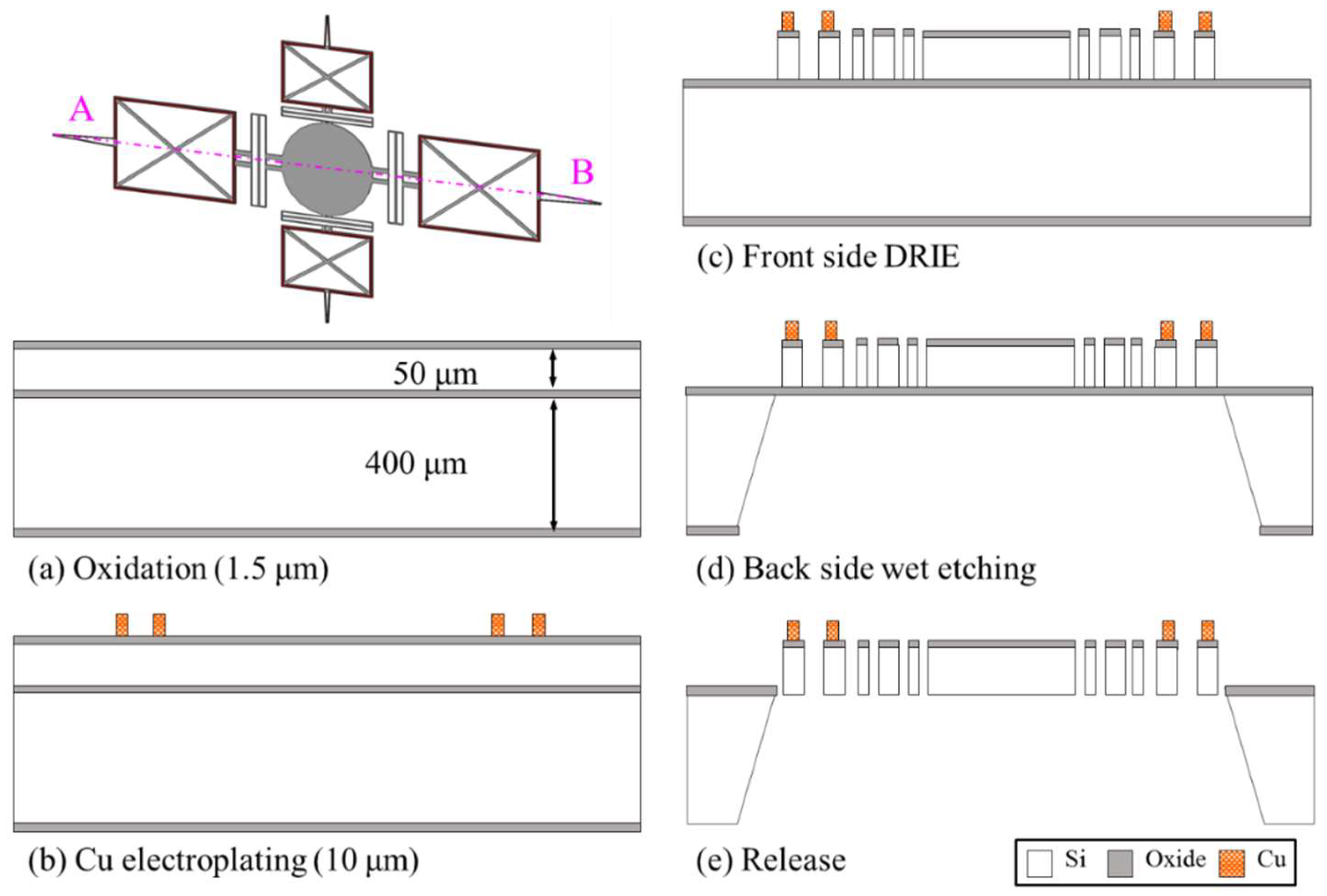
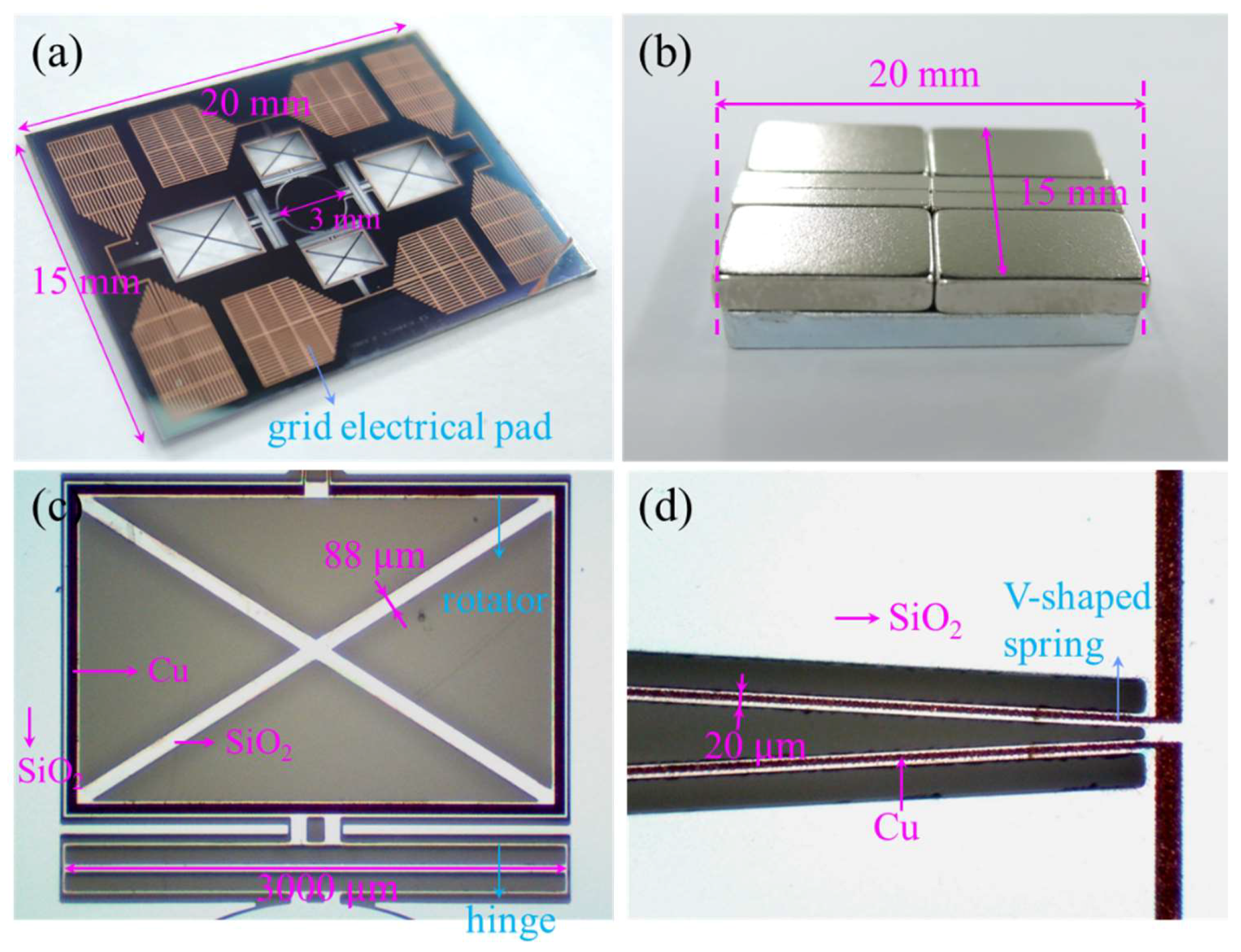
3. Fabrication
4. Results and Discussion
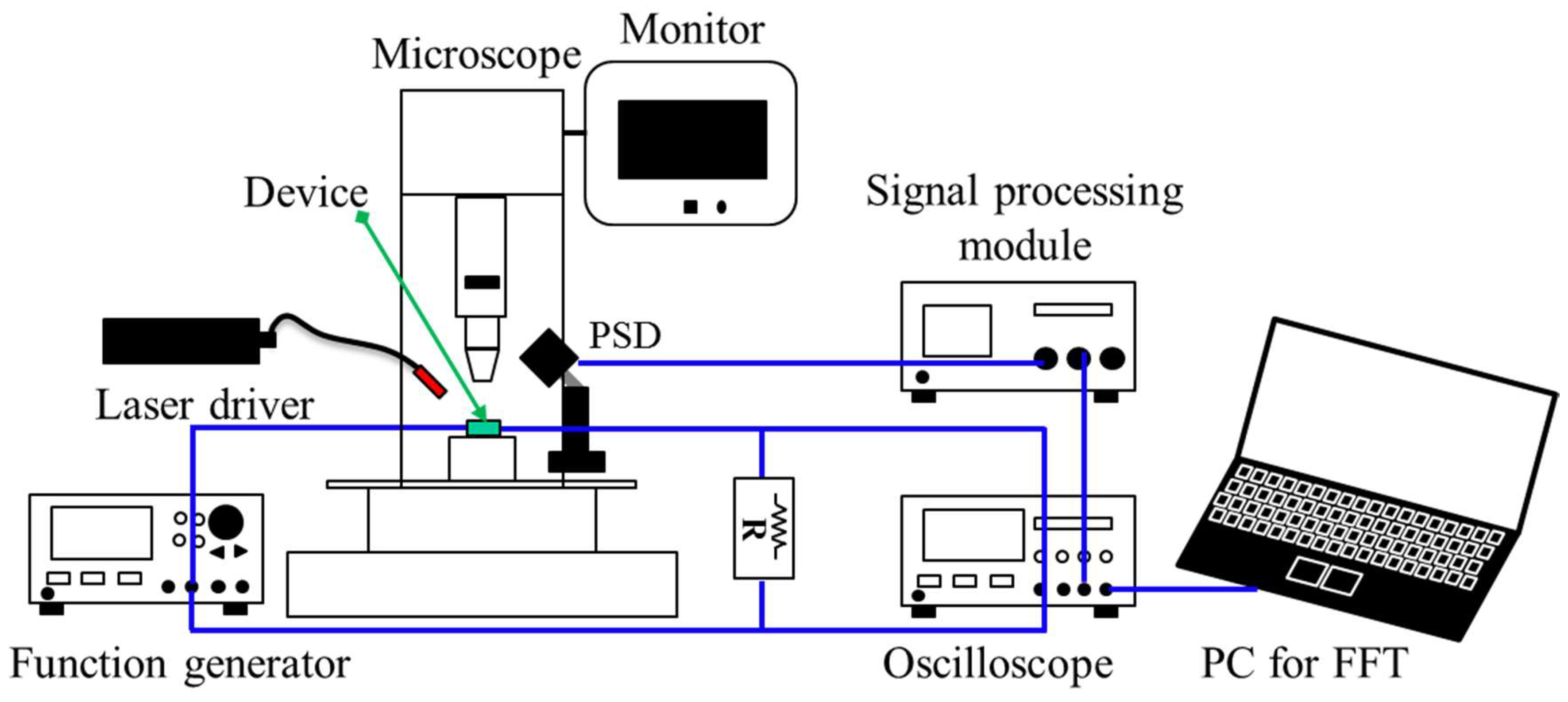
4.1. Experimental Setup
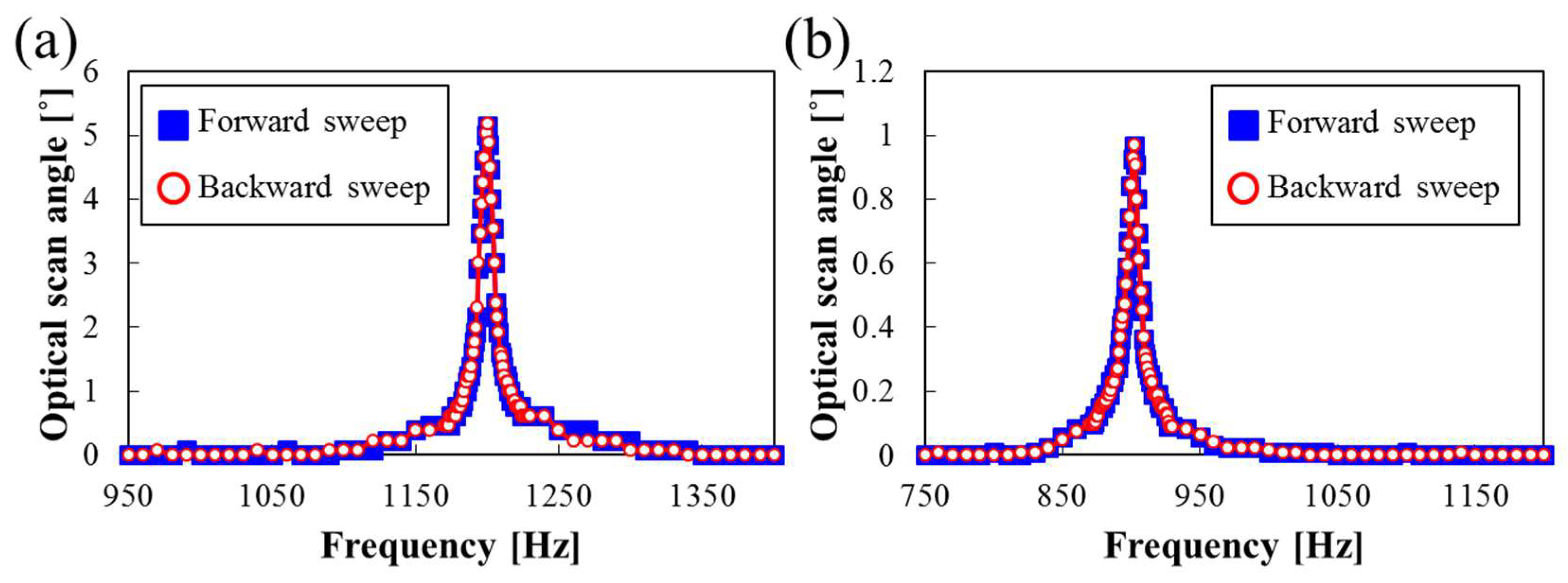
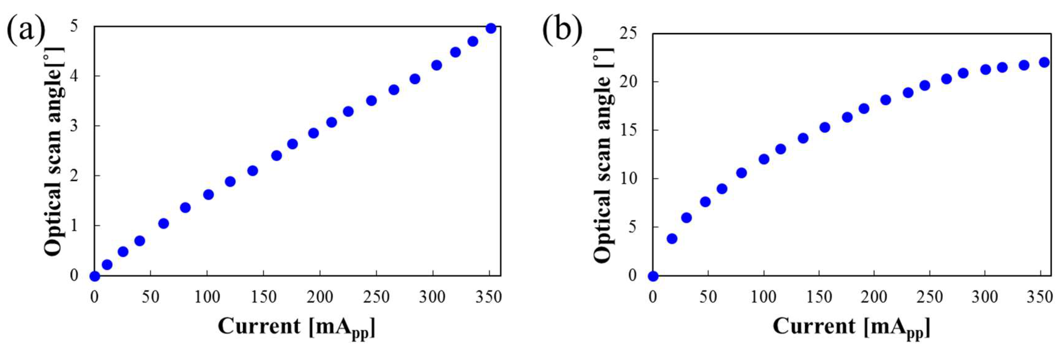
4.2. Frequency Response and Optical Scan Angle
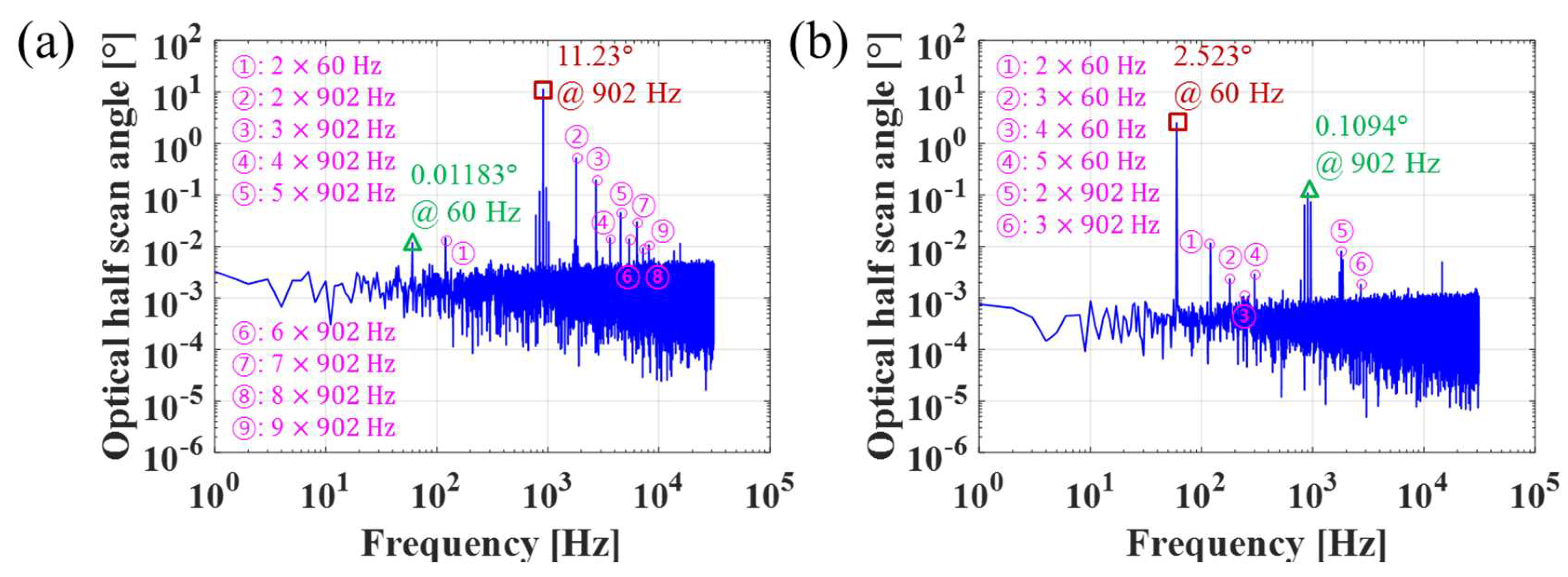
4.3. Crosstalk Analysis
5. Conclusions
Author Contributions
Acknowledgments
Conflicts of Interest
References
- Cho, A.R.; Han, A.; Ju, S.; Jeong, H.; Park, J.-H.; Kim, I.; Bu, J.-U.; Ji, C.-H. Electromagnetic biaxial microscanner with mechanical amplification at resonance. Opt. Express 2015, 23, 16792–16802. [Google Scholar] [CrossRef] [PubMed]
- Park, Y.; Moon, S.; Lee, J.; Kim, K.; Lee, S.-J.; Lee, J.H. Via-less two-axis electromagnetic micro scanner based on dual radial magnetic fields. IEEE Photonics Technol. Lett. 2018, 30, 443–446. [Google Scholar] [CrossRef]
- Fan, K.-C.; Lin, W.-L.; Chiang, L.-H.; Chen, S.-H.; Chung, T.-T.; Yang, Y.-J. A 2 × 2 mechanical optical switch with a thin mems mirror. J. Lightw. Technol. 2009, 27, 1155–1161. [Google Scholar] [CrossRef]
- Ji, C.-H.; Choi, M.; Kim, S.-C.; Song, K.-C.; Bu, J.-U.; Nam, H.-J. Electromagnetic two-dimensional scanner using radial magnetic field. J. Microelectromech. Syst. 2007, 16, 989. [Google Scholar] [CrossRef]
- Yalcinkaya, A.D.; Urey, H.; Brown, D.; Montague, T.; Sprague, R. Two-axis electromagnetic microscanner for high resolution displays. J. Microelectromech. Syst. 2006, 15, 786–794. [Google Scholar] [CrossRef]
- Tanguy, Q.A.; Bargiel, S.; Xie, H.; Passilly, N.; Barthès, M.; Gaiffe, O.; Rutkowski, J.; Lutz, P.; Gorecki, C. Design and fabrication of a 2-axis electrothermal mems micro-scanner for optical coherence tomography. Micromachines 2017, 8, 146. [Google Scholar] [CrossRef]
- Hu, Q.; Pedersen, C.; Rodrigo, P.J. Eye-safe diode laser doppler lidar with a mems beam-scanner. Opt. Express 2016, 24, 1934–1942. [Google Scholar] [CrossRef] [PubMed]
- Kim, J.; Lee, S.; Jeong, H.; Lee, S.; Ji, C.; Park, J. Electromagnetically actuated 2-axis scanning micromirror with large aperture and tilting angle for lidar applications. In Proceedings of the 2015 Transducers—2015 18th International Conference on Solid-State Sensors, Actuators and Microsystems (TRANSDUCERS), Anchorage, AK, USA, 21–25 June 2015; pp. 839–842. [Google Scholar]
- Milanovic, V.; Matus, G.A.; McCormick, D.T. Gimbal-less monolithic silicon actuators for tip-tilt-piston micromirror applications. IEEE J. Sel. Top. Quantum Electron. 2004, 10, 462–471. [Google Scholar] [CrossRef]
- Naono, T.; Fujii, T.; Esashi, M.; Tanaka, S. Non-resonant 2-d piezoelectric mems optical scanner actuated by nb doped pzt thin film. Sens. Actuators A Phys. 2015, 233, 147–157. [Google Scholar] [CrossRef]
- Zhang, X.; Duan, C.; Liu, L.; Li, X.; Xie, H. A non-resonant fiber scanner based on an electrothermally-actuated mems stage. Sens. Actuators A Phys. 2015, 233, 239–245. [Google Scholar] [CrossRef] [PubMed]
- Han, A.; Cho, A.R.; Ju, S.; Ahn, S.-H.; Bu, J.-U.; Ji, C.-H. Electromagnetic biaxial vector scanner using radial magnetic field. Opt. Express 2016, 24, 15813–15821. [Google Scholar] [CrossRef] [PubMed]
- Holmstrom, S.T.; Baran, U.; Urey, H. Mems laser scanners: A review. J. Microelectromech. Syst. 2014, 23, 259–275. [Google Scholar] [CrossRef]
- Tsuboi, O.; Mizuno, Y.; Koma, N.; Soneda, H.; Okuda, H.; Ueda, S.; Sawaki, I.; Yamagishi, F. A rotational comb-driven micromirror with a large deflection angle and low drive voltage. In Proceedings of the Fifteenth IEEE International Conference on Micro Electro Mechanical Systems, Las Vegas, NV, USA, 24 January 2002; pp. 532–535. [Google Scholar]


© 2018 by the authors. Licensee MDPI, Basel, Switzerland. This article is an open access article distributed under the terms and conditions of the Creative Commons Attribution (CC BY) license (http://creativecommons.org/licenses/by/4.0/).
Share and Cite
Park, Y.; Moon, S.; Lee, J.; Kim, K.; Lee, S.-J.; Lee, J.-H. Gimbal-Less Two-Axis Electromagnetic Microscanner with Twist Mechanism. Micromachines 2018, 9, 219. https://doi.org/10.3390/mi9050219
Park Y, Moon S, Lee J, Kim K, Lee S-J, Lee J-H. Gimbal-Less Two-Axis Electromagnetic Microscanner with Twist Mechanism. Micromachines. 2018; 9(5):219. https://doi.org/10.3390/mi9050219
Chicago/Turabian StylePark, Yangkyu, Seunghwan Moon, Jaekwon Lee, Kwanghyun Kim, Sang-Jin Lee, and Jong-Hyun Lee. 2018. "Gimbal-Less Two-Axis Electromagnetic Microscanner with Twist Mechanism" Micromachines 9, no. 5: 219. https://doi.org/10.3390/mi9050219
APA StylePark, Y., Moon, S., Lee, J., Kim, K., Lee, S.-J., & Lee, J.-H. (2018). Gimbal-Less Two-Axis Electromagnetic Microscanner with Twist Mechanism. Micromachines, 9(5), 219. https://doi.org/10.3390/mi9050219