Abstract
This work focuses on the effect of remote phonon arising from the substrate and high-κ gate dielectric on electron mobility in two-dimensional (2D) InSe field-effect transistors (FETs). The electrostatic characteristic under quantum confinement is derived by self-consistently solving the Poisson and Schrödinger equations using the effective mass approximation. Then mobility is calculated by the Kubo–Greenwood formula accounting for the remote phonon scattering (RPS) as well as the intrinsic phonon scatterings, including the acoustic phonon, homopolar phonon, optical phonon scatterings, and Fröhlich interaction. Using the above method, the mobility degradation due to remote phonon is comprehensively explored in single- and dual-gate InSe FETs utilizing SiO2, Al2O3, and HfO2 as gate dielectric respectively. We unveil the origin of temperature, inversion density, and thickness dependence of carrier mobility. Simulations indicate that remote phonon and Fröhlich interaction plays a comparatively major role in determining the electron transport in InSe. Mobility is more severely degraded by remote phonon of HfO2 dielectric than Al2O3 and SiO2 dielectric, which can be effectively insulated by introducing a SiO2 interfacial layer between the high-κ dielectric and InSe. Due to its smaller in-plane and quantization effective masses, mobility begins to increase at higher density as carriers become degenerate, and mobility degradation with a reduced layer number is much stronger in InSe compared with MoS2.
1. Introduction
The compelling demand for higher performance and lower power consumption in complementary metal-oxide-semiconductor (CMOS) field-effect transistors (FETs) has highlighted the quest for devices and architectures based on new materials [1]. Performance boosters such as strain, high-κ dielectric, metal gate, and three-dimensional (3D) devices have enabled extraordinary improvement of performance in the past 60 years [2,3]. Recently, two-dimensional (2D) van der Waals semiconductors hold great potential for optics and electronics application due to their unique properties, including the atomic thickness, tunable bandgap, and dangling-bond-free surface, which achieves improved gate control over the channel and reduced short channel effects [4,5]. So far, many classes of 2D material-based devices have been extensively studied, such as graphene, transition metal dichalcogenides (TMDs), and black phosphorus [6,7,8]. Very recently, few-layer InSe has attracted much attention due to its highly promising prospect as channel material for FETs, offering small effective mass of electron ~0.14 m0 and high electron mobility up to ~103 cm2/Vs at room temperature obtained by experimental measurements [9,10,11]. Therefore, InSe has advantages of a similar gap as silicon, 2D nature as graphene, higher mobility than TMDs, and higher environmental stability than black phosphorus. In addition, electrostatic tunability of spin-orbit coupling in InSe has been identified, showing potential in devising III-VI based spintronic devices [12,13].
However, the charge transport properties in InSe FET have not been well understood and starve for comprehensive investigation. More recently, the ballistic performance of mono- and multi-layer InSe FET is studied by the first-principles calculation and the top of the barrier model [14], and temperature-dependent phonon-limited mobility is estimated by the physical modeling of intrinsic scattering mechanisms [15]. On the other hand, charge transport behavior is very sensitive to external surroundings, such as gaseous adsorbates from air and trapped charges in substrates [16], and their electronic performance is generally lower than their intrinsic values. Previous studies of back-gated multilayer InSe FET on various substrates (bare SiO2, bare Al2O3, poly(methyl methacrylate) (PMMA)/SiO2, and PMMA/Al2O3) have reported the carrier mobility ranging from 2.2 cm2/Vs to 1055 cm2/Vs at low operating voltage [10], while dual-gated InSe FET on hexagonal boron nitride (hBN)/SiO2 show an excellent mobility approaching 103 cm2/Vs and 104 cm2/Vs at room and liquid-helium temperatures respectively [9]. It is apparently suggested that the introduction of substrate and gate dielectric has a strong effect on the electron mobility, which can be generally contributed to the extrinsic scatterings from surface roughness (SRS), interfacial Coulomb impurities (CIS), and remote phonon scatterings (RPS) [17,18]. Atomic flatness of 2D materials makes them immune to SR scattering, while CIS can be lowered or eliminated as possible by improving the fabrication process. Therefore, only remote phonon can be regarded as an intrinsic factor arising from the dielectric environment, and open questions remain as to its role in determining the electron transport in atomically-thin InSe FETs.
In this paper, the effect of remote phonons arising from the substrate and high-κ dielectric together with the intrinsic phonons of the InSe channel on electron transport is studied based on the physical modeling by self-consistently solving the Poisson and Schrödinger equations and employing the Kubo–Greenwood formula. Mobility behaviors in single-gate and dual-gate InSe FET with various gate dielectric are theoretically explored and analyzed as a function of temperature, inversion density, InSe layer number, and SiO2 interfacial layer thickness. Acoustic phonons and optical phonons—as well as homopolar phonons—have a minor effect on electron mobility, while remote phonons and Fröhlich interaction play a comparatively major role in determining the electron transport in InSe. Compared with MoS2, much smaller effective masses of electron in InSe give rise to a great enhancement of mobility at high density as carriers become degenerate. Simulation results in this work provide physical insight into the mobility behavior of InSe FET for carrier mobility optimization from the theoretical viewpoint.
This paper is organized as follows. Section 2 describes the device structures and simulation methods, especially the physical models of remote phonon depending on the gate stack. In Section 3, we present simulation results of mobility and corresponding explanations. Finally, the conclusion is drawn in Section 4.
2. Device Structures and Simulation Methods
Simulated device structures with 2D-layered InSe channel are shown in Figure 1, where the intrinsic channel without doping is assumed. Figure 1a shows the back-gate (single-gate) InSe FET with SiO2 substrate as gate dielectric. Figure 1b shows the top-gate (dual-gate) InSe FETs with high-κ dielectric as top dielectric and SiO2 substrate as back dielectric. Figure 1c shows the structure with additional SiO2 interfacial layer (ITL) embedded between the InSe channel and high-κ dielectric compared with Figure 1b. In the case of single-gate devices, only the back gate is biased with Vbg, while the back gate is grounded and the top gate is biased with Vtg for the dual-gated devices. In this work, traditionally used high-κ dielectrics of HfO2 and Al2O3 are comprehensively studied, with corresponding parameters listed in Table 1. Except for Figure 2, all the simulation results are calculated at room temperature (300 K).
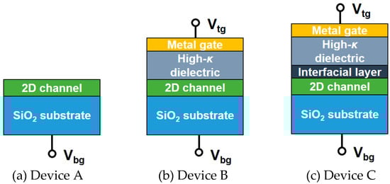
Figure 1.
Simulated device structure with atomically thin InSe channel in this work. (a) Back-gate InSe field-effect transistors (FET) with SiO2 substrate as gate dielectric. (b) Dual-gate InSe FET with high-κ dielectric as top-gate dielectric and SiO2 substrate as back-gate dielectric. (c) The same structure as (b) with additional SiO2 interfacial layer embedded between the InSe channel and high-κ dielectric. For the dual-gate structure, high-κ dielectric is covered with a metal gate.

Table 1.
Parameters for the polar phonons in some high-κ materials [20]
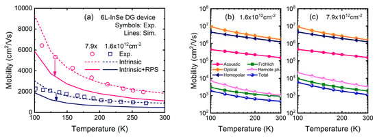
Figure 2.
Temperature-dependent mobility in six-layer InSe FETs at inversion density of 1.6 × 1012 cm−2 and 7.9 × 1012 cm−2, respectively. (a) Comparison between the experimental mobility (symbols) and calculated intrinsic mobility without remote phonon scattering (RPS) (dashed lines), which shows an excellent agreement. In contrast, the mobility with RPS (solid lines) is significantly degraded. (b,c) Contributions of each scattering mechanisms to the total mobility for different inversion density respectively. Intrinsic scatterings include acoustic (AC), optical (OP), and homopolar (HO) phonon scatterings as well as Fröhlich interaction, while extrinsic scattering is remote phonon scattering arising from the HfO2 high-κ dielectric.
We start the calculation by obtaining the electrostatic characteristic of the two-dimensional electron gas (2DEG) in InSe layer by self-consistently solving the Poisson and Schrödinger equations using the effective mass approximation with nonparabolicity correction, inherently accounting for the quantum confinement effects [19]. Particularly the energy dispersion of 2D-layered InSe is described by the thickness-dependent effective masses obtained from first-principles calculation, as shown in our previous work [14]. Next, the matrix elements and the scattering rates are calculated through the Fermi golden rule [19]. Physical models for electron mobility include the remote phonon scattering (RPS) arising from the high-κ dielectric as well as the intrinsic phonon scatterings of channel material, including the acoustic (AC) phonon-, homopolar (HO) phonon-, optical (OP) phonon- scatterings, and Fröhlich interaction (POP) [20,21,22,23]. For AC phonons, elastic and isotropic approximations are adopted. The HO and OP scatterings are treated as inelastic and isotropic process. For POP and RP scatterings, inelastic and anisotropic characteristic are considered. Once the scattering rates are obtained, the mobility is calculated by the Kubo–Greenwood formula employing the momentum relaxation time approximation. The parameters for mobility calculation in few-layer InSe are taken from our previous work [15].
For remote phonon induced by SiO2 substrate, the semi-infinite substrate is assumed, and the dispersion relationship for the remote phonon model can be written as [19]
where ωTO1,SiO2 is the low-frequency phonon mode of SiO2, εInSe is the dielectric constant of InSe. The potential amplitude of the remote phonon is written as
For the remote phonon induced by top gate dielectric, high-κ dielectric covered with a metal gate is employed in the simulation. As shown in Table 1, the frequencies of two polar phonons in high-κ dielectrics such Al2O3 and HfO2 show great discrepancy. Hence, for simplicity, only the low-frequency phonon mode in high-κ gate dielectric is considered [19]. For high-κ dielectric with a metal gate as shown in Figure 1b, the dispersion relationship is
where ωTO1,HK is the low-frequency phonon mode of high-κ dielectric, εHK,0 and εHK,int are the dielectric constant at the static and intermediate frequency, THK is the thickness of top gate dielectric, and q = |k − k′| is the remote phonon momentum. The effective dielectric constant depending on the frequency dependent dielectric constant of the high-κ material can be written as
and then the corresponding potential amplitude is
For the high-κ gate stack with a SiO2 interfacial layer, namely ITL/high-κ/metal-gate stack as shown in Figure 1c, the dispersion relationship is [16]
where TITL is the thickness of interfacial layer. The effective dielectric constant is
Then the potential amplitude for the ITL/high-κ/metal-gate stack can be obtained through the Equations (5) and (7).
3. Results and Discussion
To begin with, we calibrate the physical models with the experimental measurement. Figure 2 shows the calculated and experimental temperature-dependent mobility at inversion density of 1.6 × 1012 cm−2 and 7.9 × 1012 cm−2 in six-layer InSe dual-gate FET. It should be noted that the experiment results are obtained from the dual-gate InSe FET with channel covered by hexagonal boron nitride (hBN) [9], which insulates InSe from the dielectric environment, leading to the absence of remote phonon scattering. From Figure 2a, considering the intrinsic scatterings by AC, HO, and OP phonon and Fröhlich interaction, the temperature-dependent electron mobility curves measured by Hall effect are reproduced successfully for T > 100 K, where phonon scatterings dominate. The excellent agreement between the simulations and experiments validate our methods and models. It should be pointed out that when temperature is down to 100 K, there is a significant discrepancy of mobility between simulations and experiments due to the fact that Coulomb scattering resulting from the channel impurities and interfacial charges is excluded, which is a dominant factor in determining the carrier mobility in the low-temperature regime.
On the other hand, if high-κ dielectric of HfO2 is directly deposited on the InSe channel, the mobility is severely degraded from its intrinsic value, as shown in Figure 2a by solid lines. For example, at room temperature, mobility changes from 1808 to 1120 cm2/Vs (920 to 464 cm2/Vs) at inversion density of 7.9 × 1012 cm−2 (1.6 × 1012 cm−2) due to the remote phonon scattering. To understand the mobility behavior in depth, Figure 2b,c plot the contributions of all the considered scattering mechanisms to the total mobility. Compared with AC, OP, and HO phonons, the remote phonon together with Fröhlich interaction plays a comparatively major role in determining the electron transport in InSe FET. This is the objective of this work to focus on the remote phonon scattering in InSe FET with high-κ gate stack in the following.
The effect of remote phonon originating from the substrate and gate stack on the electron transport of few-layer InSe is shown in Figure 3. The intrinsic phonon-limited mobility in six-layer single-gate InSe FET is ~843 cm2/Vs at low inversion density. With SiO2 substrate employed, the mobility is degraded to ~735 cm2/Vs due to remote phonon. In the case of dual-gate structure, when Al2O3 and HfO2 are used as top-gate dielectric, the additional remote phonon further reduces the mobility to ~634 cm2/Vs and 426 cm2/Vs respectively. It can be seen that the HfO2 dielectric has a much stronger influence of remote phonon than Al2O3 and SiO2 dielectric since it has higher dielectric constant and softer polar vibration mode [20], as listed in Table 1. Particularly, it is worth noting that the smaller permittivity of InSe results in a stronger remote phonon coupling with electrons compared with silicon even in the SiO2 case. Despite serious degradation due to remote phonons, the mobility of the six-layer InSe with high-κ dielectric is higher than that of silicon on insulator (SOI) device with SiO2 dielectric at a comparative thickness [24], revealing its great potential in high-performance logic application.
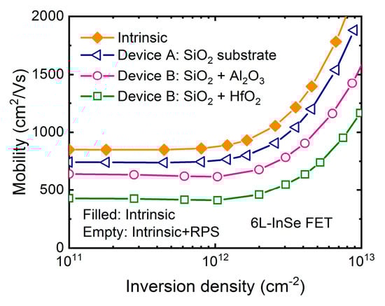
Figure 3.
Calculated mobility as a function of inversion density in six-layer InSe FETs with different device structures as shown in Figure 1a,b utilizing Al2O3 and HfO2 as top-gate dielectric and SiO2 substrate as back-gate dielectric respectively. Equivalent oxide thickness (EOT) = 1 nm of high-κ dielectric is assumed. Filled symbols represent intrinsic phonon-limited mobility for benchmark, while empty symbols represent total mobility including the remote phonon scattering from substrate and high-κ dielectric.
It is also observed that in six-layer InSe, mobility is increased significantly at higher density, which is against the common sense. To confirm this behavior, mobility in 2-, 6-, 16-, and 40-layer InSe FET is calculated in Figure 4a,b, where HfO2 and Al2O3 dielectric are used separately. At the same time, mobility in MoS2 FET using same device structure is also plotted in Figure 4c,d for comparison. In the MoS2 case, as inversion density increases, mobility monotonously decreases for thick devices as expected, and remains almost unchanged for thin devices due to strong quantum confinement. In the InSe case, at low density, mobility behavior is consistent with MoS2. However, when inversion density is larger than ~2 × 1012 cm−2, mobility quickly increases regardless of layer number or high-κ dielectric. Actually, this is also demonstrated by experimental results in [9] as shown in Figure 2a, which cannot be totally contributed to impurity scattering because at large inversion density and room temperature the screening produced by the inversion layer drastically reduce the Coulomb scattering. Therefore, this exceptional enhancement seems intrinsic for 2D-layered InSe to a great extent.

Figure 4.
Mobility as a function of inversion density with layer number of 2, 6, 16, and 40 employing the dual-gate structure as shown in Figure 1b in InSe and MoS2 FET for comparison. EOT = 1 nm of high-κ dielectric is assumed. (a) InSe FET with HfO2 dielectric. (b) InSe FET with Al2O3 dielectric. (c) MoS2 FET with HfO2 dielectric. (d) MoS2 FET with Al2O3.
To get physical insight into this mobility behavior, Figure 5a–d shows the contributions of each scattering mechanism to the total mobility in both InSe and MoS2 FET with 2- and 40-layer thickness respectively. Consistent with above-mentioned results, mobility behavior is mainly governed by the remote phonon and Fröhlich interaction in all considered devices. We find that their scattering rates increase with inversion density increasing, which should reduce the mobility. In the MoS2 case, carriers are always non-degenerate following the Boltzmann distribution, where the mobility is essentially determined by the relaxation times or scattering rates. On the other hand, when inversion density is larger than ~2 × 1012 cm−2, carriers in InSe FET become degenerate, where subband minimum is lower than Fermi level EF, and consequently the most influential relaxation times are those for energies close to EF. Due to their anisotropic property, scattering rates of remote phonon and Fröhlich interaction are much smaller near EF than those of the subband minimum, giving rise to an enhancement of mobility. This discrepancy between InSe and MoS2 FET can be well understood by their effective masses. Firstly, in-plane effective mass of 0.14 m0 in InSe is much smaller than 0.62 m0 in MoS2 [25] leading to much smaller density-of-states (DOS). In order to obtain the same density, the conduction band minimum is lower than Fermi level over a few kBT, where kB is the Boltzmann constant. Secondly, quantization effective mass of 0.08 m0 in InSe is also much smaller than 0.49 m0 in MoS2 [26]. This is the reason that quantum confinement takes effect in 16-layer InSe, but not until the layer number is reduced to 6 layers in MoS2. Actually, less subbands contributing to the carrier transport in InSe need Fermi level being higher to change the density, which makes carriers more degenerate together with the effect of small DOS.
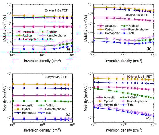
Figure 5.
Contributions of each scattering process to the total mobility corresponding to Figure 4a,c for InSe and MoS2 FET with HfO2 dielectric respectively. (a) 2-layer InSe FET. (b) 40-layer InSe FET. (c) 2-layer MoS2 FET. (d) 40-layer MoS2 FET.
The dependence of mobility on number of layer (NL) in InSe FET is shown in Figure 6a, where inversion densities of 5 × 10¹¹, 2 × 10¹², and 8 × 1012 cm−2 are considered respectively. In the case of the relatively medium and high density, mobility is almost independent of channel thickness until NL ~15, and then drops rapidly as NL is further reduced. In the low-density case, mobility degradation occurs earlier when NL <40. It is noted that for thicker devices, mobility at 5 × 1011 cm−2 gradually surpasses the value at 2 × 1012 cm−2 and then reaches up to the value at 8 × 1012 cm−2. This awkward behavior can be explained by Figure 4a,b, where mobility initially decrease and then the trend is opposite at higher density, as inversion density decreases in the 40-layer InSe FET. To get physical insight into the mobility degradation, contributions of each scattering mechanism at 5 × 1011 cm−2 is shown in Figure 6b. AC-, LO-, and HO-limited mobility is severely reduced when NL is less than ~15, while the degradation of remote-phonon as well as Fröhlich-limited mobility begins to decrease about NL ~40, further indicating their major role in determining the electron transport.
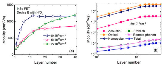
Figure 6.
(a) Mobility as a function of number of layers ranging from 1 to 40 with different inversion density in InSe FET using HfO2 as gate dielectric and SiO2 as substrate, as shown in Figure 1b. (b) Contributions of each scattering mechanism to the total mobility at low inversion density.
Inspired by the similar situation for silicon [27,28], it is suggested that an interfacial layer can be introduced between InSe channel and high-κ dielectric. To explore the effect of the interfacial layer, Figure 7 shows the calculated mobility in InSe FET with device structure of Figure 1c capped with different high-κ dielectric. From Figure 7a, it can be seen that the interfacial layer effectively insulates the channel away from the high-κ dielectric, resulting in significant mobility enhancement in the whole range of inversion density due to weaker remote phonon coupling. As interfacial layer thickness is increased, more mobility enhancement is achieved until TITL approaches ~2 nm, when remote phonon from high-κ dielectric is totally separated, as shown in Figure 7b. Besides, a thin interfacial layer is more effective in HfO2 dielectric compared with Al2O3 dielectric. Figure 8 shows the corresponding remote coulomb scattering (RCS)-limited mobility as a function of SiO2 interfacial layer thickness, showing an exponential dependence on TITL as μRPS∝exp(2kFTITL), whatever the inversion density or high-κ dielectric is, with Fermi wavelength 2kF = 1.1 nm−1. This is in agreement with theoretical predictions for a remote scattering mechanism [20,28].

Figure 7.
(a) Mobility as a function of inversion density featuring different SiO2 interfacial layer thickness in InSe FET with dual-gate structure of Figure 1c. (b) Mobility as a function of SiO2 interfacial layer thickness at different inversion density in both Al2O3- and HfO2-gated InSe FET. EOT = 1 nm of high-κ dielectric is used in the simulation.
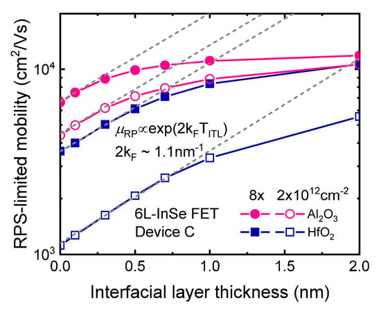
Figure 8.
Remote coulomb scattering (RCS)-limited mobility as a function of SiO2 interfacial layer thickness corresponding to total mobility in Figure 7b, showing an exponential dependence on TITL as exp(2kFTITL) with 2kF = 1.1 nm−1, represented by the dashed lines.
4. Conclusions
Based on the self-consistent Poisson and Schrödinger equations and the Kubo–Greenwood formula, remote phonons arising from both the SiO2 substrate and high-κ dielectrics in InSe FETs are comprehensively studied, together with the intrinsic scatterings by AC phonons, OP phonons, HO phonons, and Fröhlich interaction. It is observed that remote phonons and Fröhlich interaction plays a comparatively major role in determining the electron transport in InSe. Mobility is more severely degraded by remote phonon of HfO2 dielectric than Al2O3 and SiO2 dielectric, which can be effectively insulated by introducing a SiO2 interfacial layer between the high-κ dielectric and InSe. Due to its smaller in-plane and quantization effective masses, mobility begins to increase at higher densities as carriers degenerate, and mobility degradation with reduced layer number is much stronger in InSe compared with MoS2.
Author Contributions
Conceptualization, P.C.; Formal analysis, P.C.; Funding acquisition, P.C.; Investigation, P.C.; Methodology, P.C. and F.L.; Resources, X.L.; Software, P.C.; Supervision, X.L. and G.D.; Validation, P.C.; Writing—Original Draft, P.C.
Funding
This research was funded by China Postdoctoral Science Foundation (grant number 2018M630034) and National Natural Science Foundation of China (grant numbers 61804003, 61674008, 61421005).
Conflicts of Interest
The authors declare no conflict of interest.
References
- Bernstein, K.; Cavin, R.K.; Porod, W.; Seabaugh, A.; Welser, J. Device and Architecture Outlook for Beyond CMOS Switches. Proc. IEEE 2010, 98, 2169–2184. [Google Scholar] [CrossRef]
- Mistry, K.; Allen, C.; Auth, C.; Beattie, B.; Bergstrom, D.; Bost, M.; Brazier, M.; Buehler, M.; Cappellani, A.; Chau, R.; et al. A 45nm Logic Technology with High-κ+Metal Gate Transistors, Strained Silicon, 9 Cu Interconnect Layers, 193nm Dry Patterning, and 100% Pb-free Packaging. In Proceedings of the IEEE International Electron Devices Meeting, Washington, DC, USA, 10–12 December 2007. [Google Scholar] [CrossRef]
- Natarajan, S.; Agostinelli, M.; Akbar, S.; Bost, M.; Bowonder, A.; Chikarmane, V.; Chouksey, S.; Dasgupta, A.; Fischer, K.; Fu, Q.; et al. A 14nm Logic Technology Featuring 2nd-Generation FinFET Transistors, Air-Gapped Interconnects, Self-Aligned Double Patterning and a 0.0588μm2 SRAM cell size. In Proceedings of the IEEE International Electron Devices Meeting, San Francisco, CA, USA, 15–17 December 2014. [Google Scholar] [CrossRef]
- Fiori, G.; Bonaccorso, F.; Iannaccone, G.; Palacios, T.; Neumaier, D.; Seabaugh, A.; Banerjee, S.K.; Colombo, L. Electronics based on two-dimensional materials. Nat. Nanotechnol. 2014, 9, 768–779. [Google Scholar] [CrossRef] [PubMed]
- Novoselov, K.S.; Mishchenko, A.; Carvalho, A.; Castro Neto, A.H. 2D materials and van der Waals heterostructures. Science 2016, 353, 439. [Google Scholar] [CrossRef] [PubMed]
- Novoselov, K.S.; Geim, A.K.; Morozov, S.V.; Jiang, D.; Zhang, Y.; Dubonos, S.V.; Grigorieva, I.V.; Firsov, A.A. Electric Field Effect in Atomically Thin Carbon Films. Science 2004, 306, 666–669. [Google Scholar] [CrossRef]
- Schmidt, H.; Wang, S.; Chu, L.; Toh, M.; Kumar, R.; Zhao, W.; Castro Neto, A.H.; Martin, J.; Adam, S.; Ozylimaz, B.; et al. Transport Properties of Monolayer MoS2 Grown by Chemical Vapor Deposition. Nano Lett. 2014, 14, 1909–1913. [Google Scholar] [CrossRef] [PubMed]
- Li, L.; Yu, Y.; Ye, G.J.; Ge, Q.; Ou, X.; Wu, H.; Feng, D.; Cheng, X.H.; Zhang, Y. Black phosphorus field-effect transistors. Nat. Nanotechnol. 2014, 9, 372–377. [Google Scholar] [CrossRef] [PubMed]
- Bandurin, D.A.; Tyurnina, A.V.; Yu, G.L.; Mishchenko, A.; Zólyomi, V.; Morozov, S.V.; Kumar, R.K.; Gorbachev, R.V.; Kudrynskyi, Z.R.; Pezzini, S.; et al. High Electron Mobility, Quantum Hall Effect and Anomalous Optical Response in Atomically Thin InSe. Nat. Nanotechnol. 2017, 9, 223–227. [Google Scholar] [CrossRef] [PubMed]
- Feng, W.; Zheng, W.; Cao, W.; Hu, P. Back Gated Multilayer InSe Transistors with Enhanced Carrier Mobilities via the Suppression of Carrier Scattering from a Dielectric Interface. Adv. Mater. 2014, 26, 6587–6593. [Google Scholar] [CrossRef] [PubMed]
- Sucharitakul, S.; Goble, N.J.; Kumar, U.R.; Sankar, R.; Bogorad, Z.A.; Chou, F.-C.; Chen, Y.-T.; Gao, X.P.A. Intrinsic Electron Mobility Exceeding 103 cm2/(Vs) in Multilayer InSe FETs. Nano Lett. 2015, 15, 3815–3819. [Google Scholar] [CrossRef]
- Premasiri, K.; Radha, S.K.; Sucharitakul, S.; Kumar, U.R.; Sankar, R.; Chou, F.-C.; Chen, Y.-T.; Gao, X.P.A. Tuning Rashba Spin-Orbit Coupling in Gated Multilayer InSe. Nano Lett. 2018, 18, 4403–4408. [Google Scholar] [CrossRef]
- Zeng, J.; Liang, S.-J.; Gao, A.; Wang, Y.; Pan, C.; Wu, C.; Liu, E.; Zhang, L.; Cao, T.; Liu, X.; et al. Gate-tunnable weak antilocalization in a few-layer InSe. Phys. Rev. B 2018, 98, 125414. [Google Scholar] [CrossRef]
- Chang, P.; Liu, X.; Liu, F.; Du, G. First-principles based ballistic transport simulation of monolayer and few-layer InSe FET. Jpn. J. Appl. Phys. 2018. under review. [Google Scholar]
- Chang, P.; Liu, X.; Liu, F.; Du, G. Phonon-Limited Mobility in n-Type Few-Layer InSe Devices from First Principles. IEEE Electron Devices Lett. 2018. [Google Scholar] [CrossRef]
- Li, S.-L.; Tsukagoshi, K.; Orgiu, E.; Samori, P. Charge transport and mobility engineering in two-dimensional transition metal chalcogenide semiconductors. Chem. Soc. Rev. 2016, 45, 118–151. [Google Scholar] [CrossRef] [PubMed]
- Li, S.-L.; Wakabayashi, K.; Xu, Y.; Nakaharai, S.; Komatsu, K.; Li, W.-W.; Lin, Y.-F.; Ferreira, A.A.; Tsukagoshi, K. Thickness-Dependent Interfacial Coulomb Scattering in Atomically Thin Field-Effect Transistors. Nano Lett. 2013, 13, 3546–3552. [Google Scholar] [CrossRef]
- Zeng, L.; Xin, Z.; Chen, S.; Du, G.; Kang, J.; Liu, X. Remote phonon and impurity screening effect of substrate and gate dielectric on electron dynamics in single layer MoS2. Appl. Phys. Lett. 2013, 103, 113505. [Google Scholar] [CrossRef]
- Esseni, D.; Palestri, P.; Selmi, L. Nanoscale MOS Transistors: Semi-Classical Transport and Applications; Cambridge University Press: New York, NY, USA, 2011; pp. 98–103. [Google Scholar]
- Fischetti, M.V.; Neumayer, D.A.; Cartier, E.A. Effective electron mobility in Si inversion layers in metal-oxide-semiconductor systems with a high-κ insulator: The role of remote phonon scattering. J. Appl. Phys. 2001, 90, 4587–4606. [Google Scholar] [CrossRef]
- Poljak, M.; Jovanovié, V.; Grgec, D.; Suligoj, T. Assessment of Electron Mobility in Ultrathin-Body InGaAs-on-Insulator MOSFETs Using Physics-Based Modeling. IEEE Trans. Electron Devices 2012, 59, 1636–1643. [Google Scholar] [CrossRef]
- Chang, P.; Liu, X.; Zeng, L.; Wei, K.; Du, G. Investigation of Hole Mobility in Strained InSb Ultrathin Body pMOSFETs. IEEE Trans. Electron Devices 2015, 62, 947–954. [Google Scholar] [CrossRef]
- Chang, P.; Liu, X.; Du, G.; Zhang, X. Assessment of Hole Mobility in Strained InSb, GaSb and InGaSb Based Ultra-Thin Body pMOSFETs with Different Surface Orientations. In Proceedings of the IEEE International Electron Devices Meeting, San Francisco, CA, USA, 15–17 December 2014. [Google Scholar] [CrossRef]
- Tsutsui, G.; Hiramoto, T. Mobility and Threshold-Voltage Comparison Between (110)- and (100)-Oriented Ultrathin-Body Silicon MOSFETs. IEEE Trans. Electron Devices 2006, 53, 2582–2588. [Google Scholar] [CrossRef]
- Gonzalez-Medina, J.M.; Ruiz, F.G.; Martin, E.G.; Godoy, A.; Gámiz, F. Simulation study of the electron mobility in few-layer MoS2 metal-insulator-semiconductor field-effect transistors. Solid-State Electron. 2015, 114, 30–34. [Google Scholar] [CrossRef]
- Segura, A.; Marí, B.; Martinez-Pastor, J. Three-dimensional electrons and two-dimensional electric subbands in the transport properties of tin-doped n-type indium selenide: Polar and homopolar phonon scattering. Phys. Rev. B 1991, 43, 4953–4965. [Google Scholar] [CrossRef]
- Chau, R.; Datta, S.; Doczy, M.; Doyle, B.; Kavalieros, J.; Metz, M. High-κ/Metal-Gate Stack and Its MOSFET Characteristics. IEEE Electron Device Lett. 2004, 6, 408–410. [Google Scholar] [CrossRef]
- Cassé, M.; Thevenod, L.; Guillaumot, B.; Tosti, L.; Martin, F.; Mitard, J.; Weber, O.; Andrieu, F.; Ernst, T.; Reimbold, G.; et al. Carrier Transport in HfO2/Metal Gate MOSFETs: Physical Insight into Critical Parameters. IEEE Trans. Electron Devices 2006, 53, 759–768. [Google Scholar] [CrossRef]
© 2018 by the authors. Licensee MDPI, Basel, Switzerland. This article is an open access article distributed under the terms and conditions of the Creative Commons Attribution (CC BY) license (http://creativecommons.org/licenses/by/4.0/).