
Compensation Method for Die Shift Caused by Flow Drag Force in Wafer-Level Molding Process

Abstract
:
1. Introduction
- WLP is achieved by implementing a 3D package, and it enables performance enhancement through a high pin count, an extension of existing silicon technologies, a reduction in device size, and a reduction in wiring delay.
- Depending on the possibility of flexible process combinations, system semiconductors can be implemented.
- WLP is an emerging packaging process technology that allows for high-performance semiconductor production and reductions in manufacturing cost.
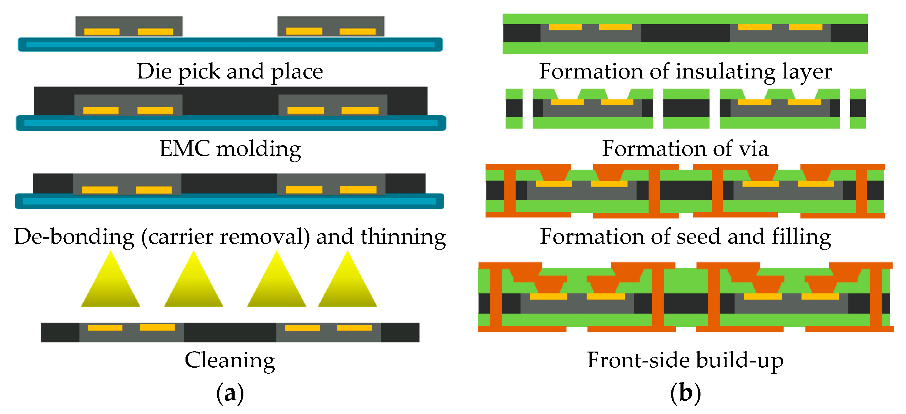
2. Molding Process of Wafer-Level Packaging
2.1. Molding Process
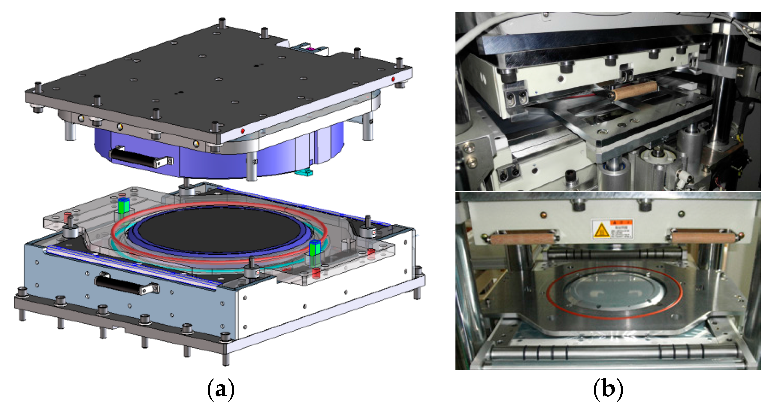
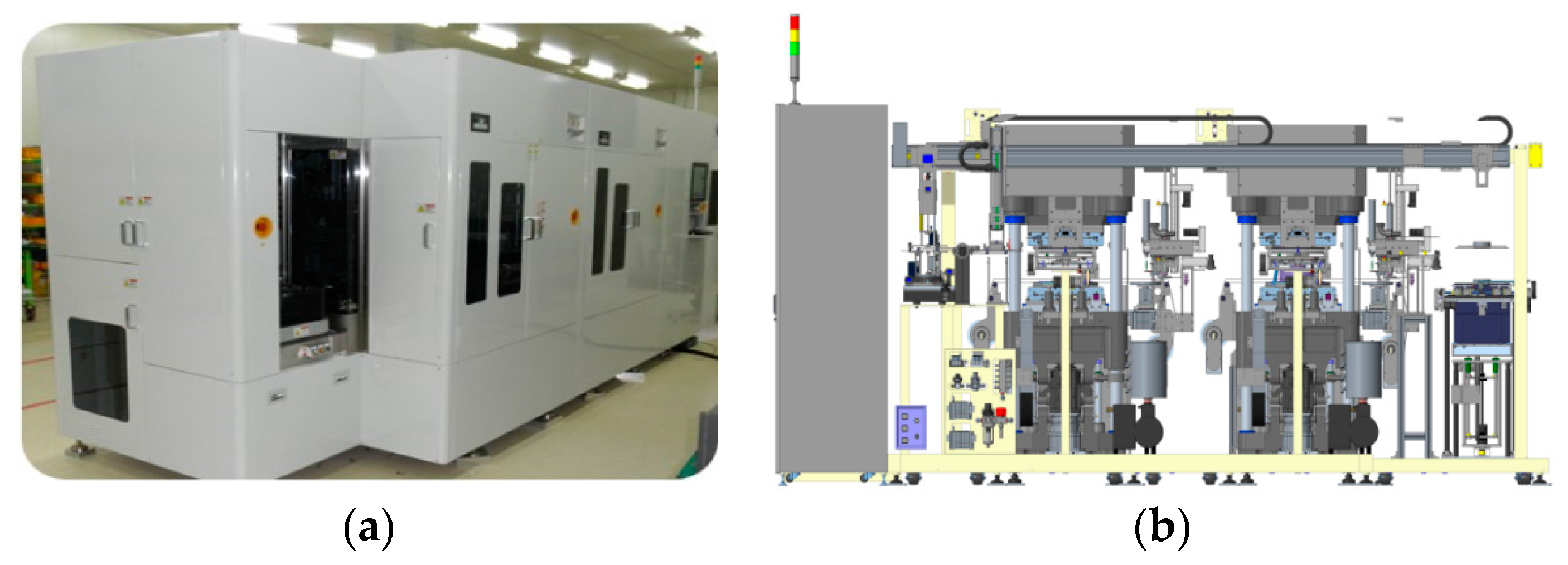
2.2. Wafer-Level Compression Molding System
- Mechanical press module: the maximum loading capacity is 100 tons, and the pressing mechanism is toggle-type
- Compression mold module: upper and lower molds are controlled at different temperatures
- Auto supply and recovery module of the release film
- Wafer loading and unloading module
- Post-curing and cooling module
- Automatic process control module
2.3. Wafer-Level Compression Mold Module
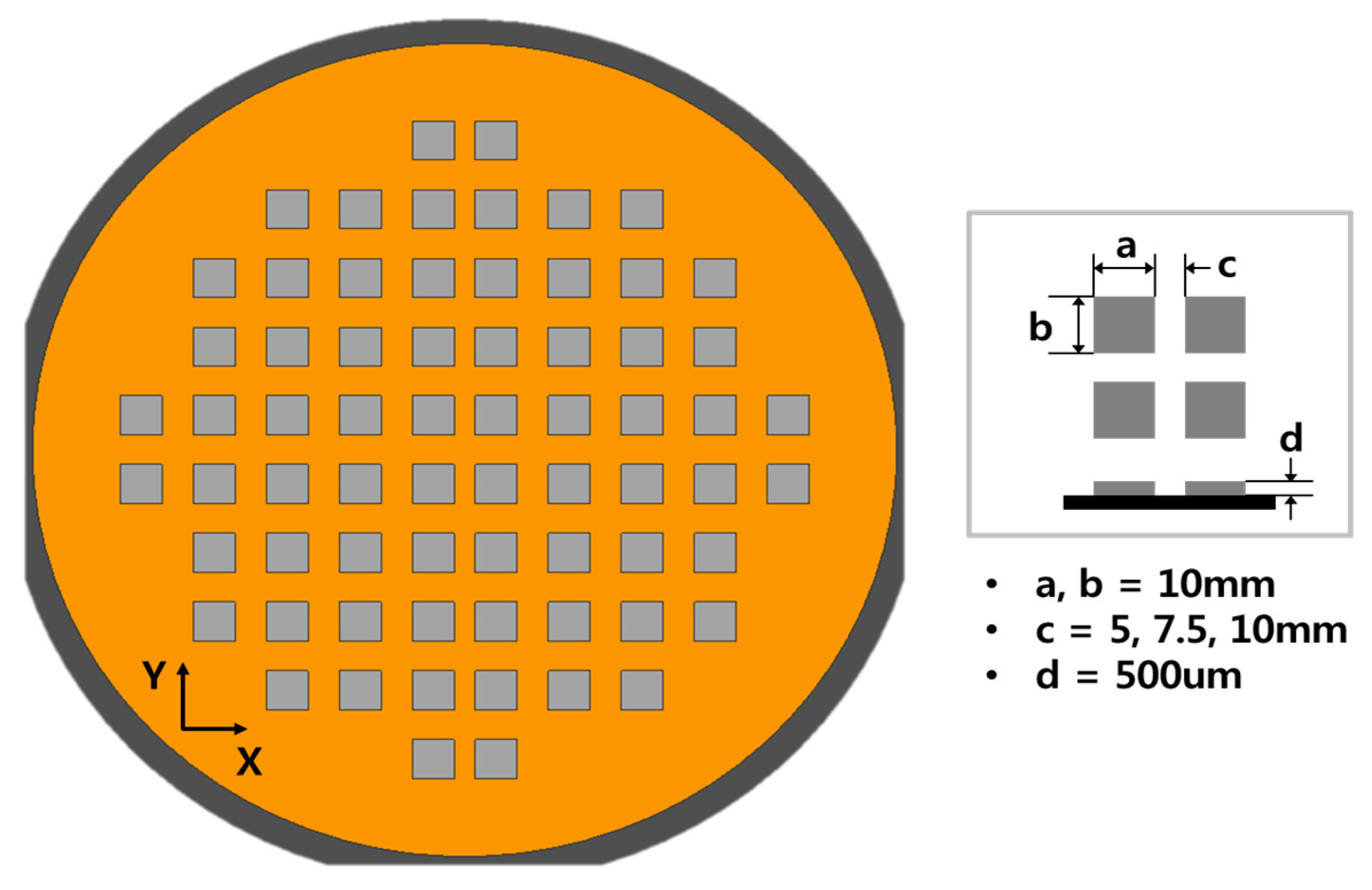
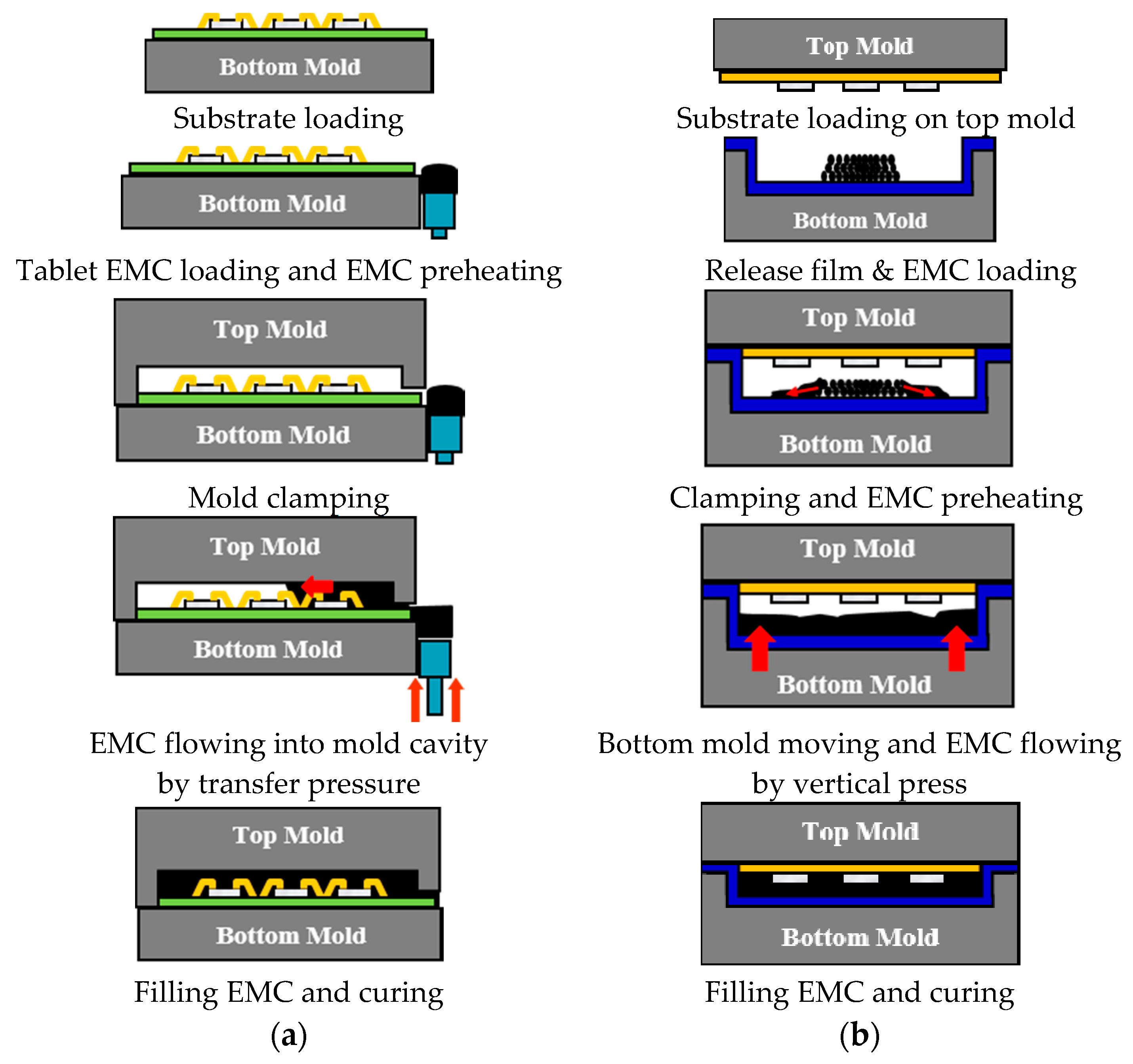
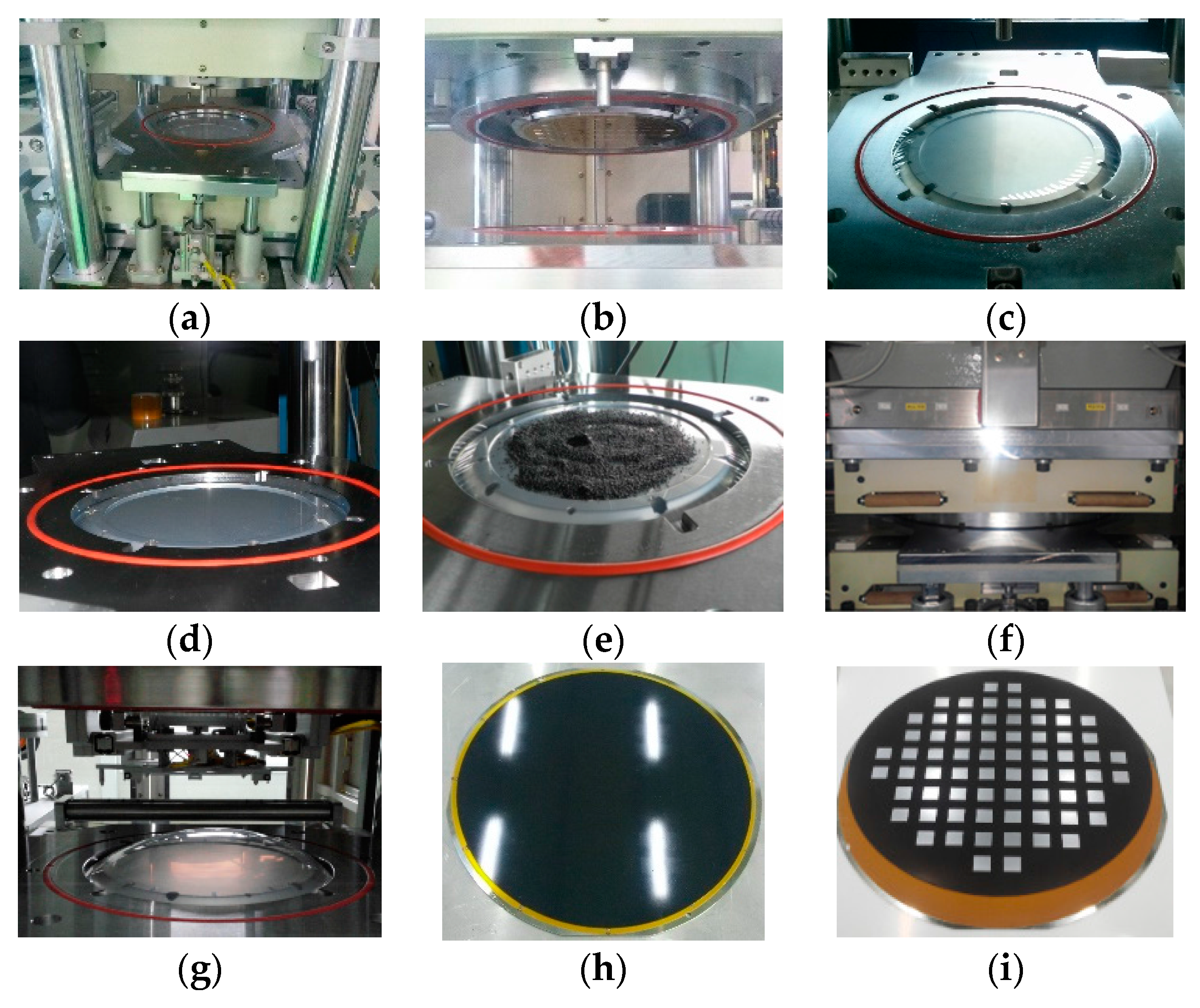
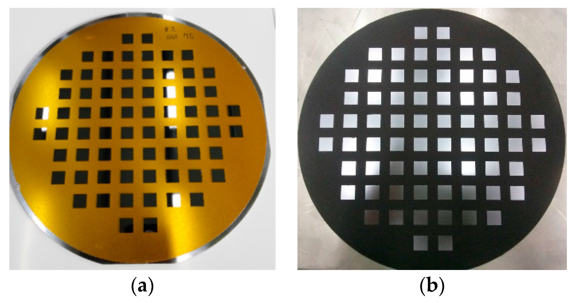
3. Molding Process Experiment
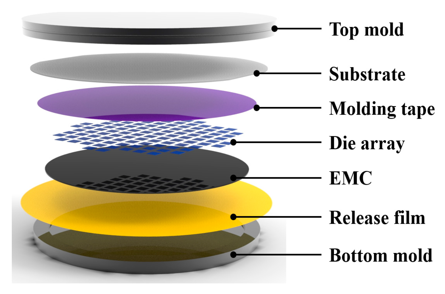
- Place the release film on the lower mold maintained at a temperature of 170 °C.
- Attach the die-arranged substrate to the upper mold using vacuum.
- Perform release film binding using the release film support plate.
- Attach the release film on the lower mold using vacuum.
- Apply granular EMC on top of the release film.
- Maintain the pressing force at 30 tons for 2 min until the forming process is completed.
- Open the mold after the curing time.
- Unload the molded wafer from the molding system, and perform the post-curing process for 1 h at 170 °C.
- Debond the molded wafer on the substrate at 200 °C.
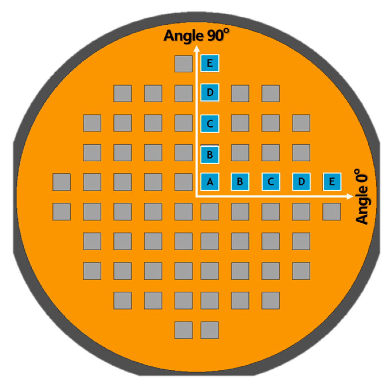
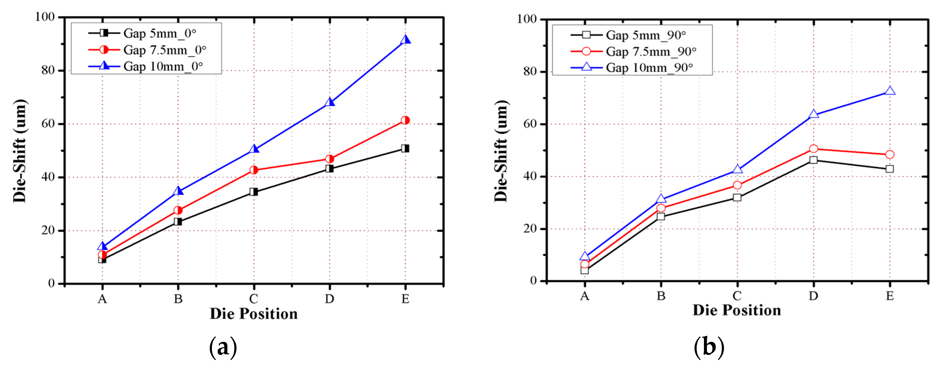
4. Experimental and Analytical Results
5. Conclusions
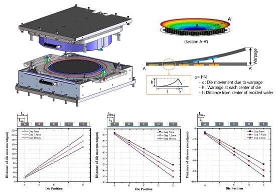
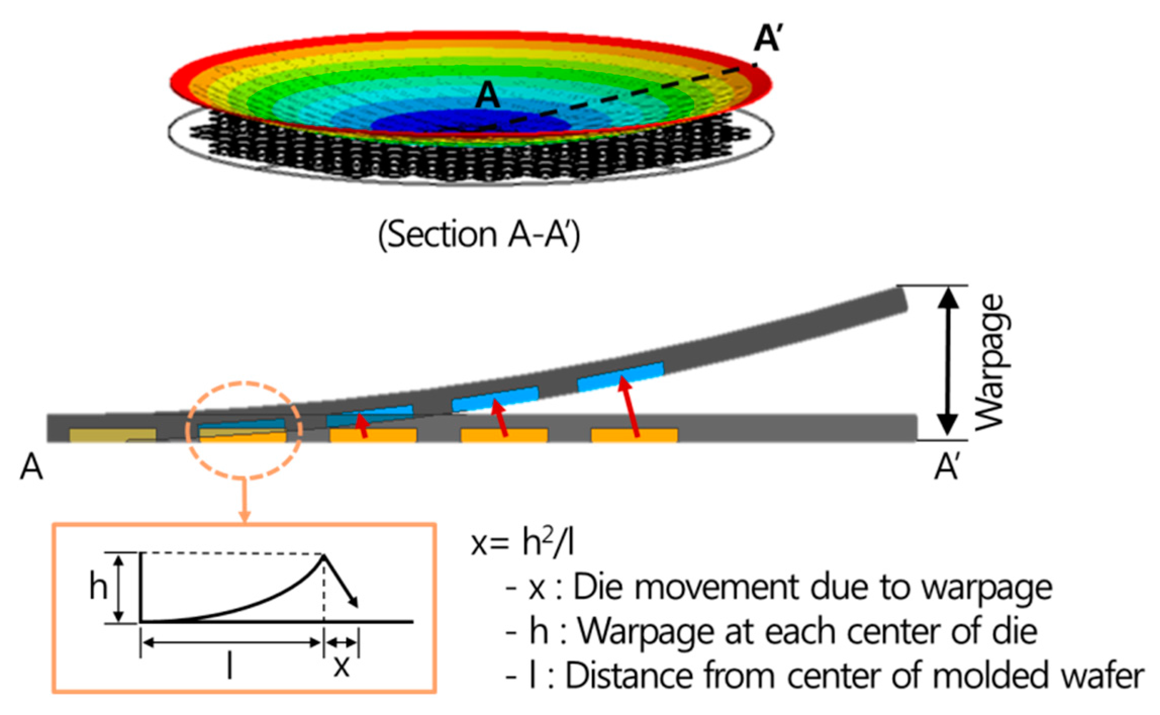
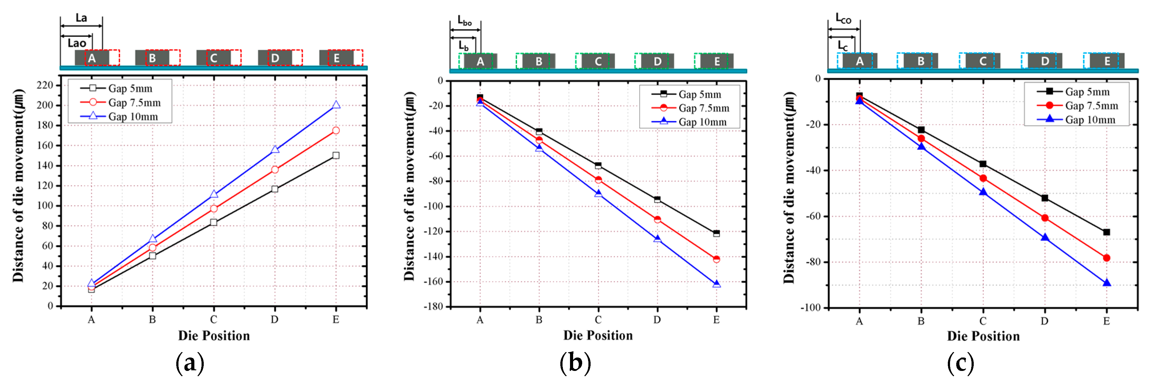
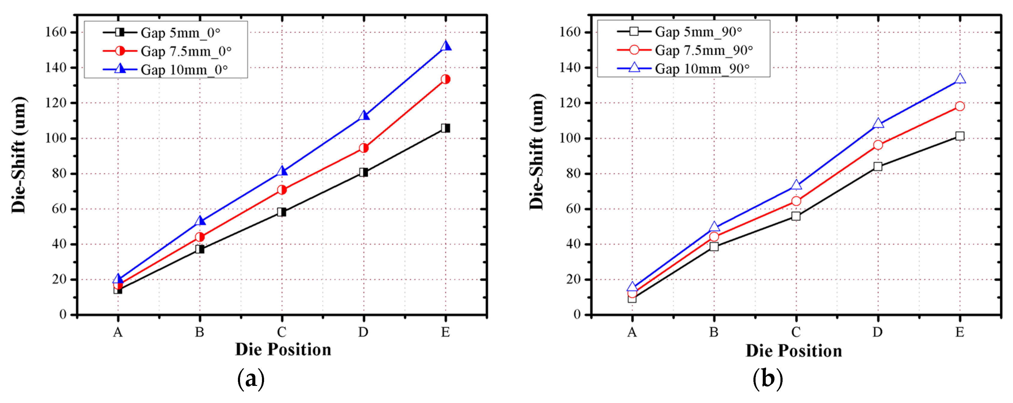
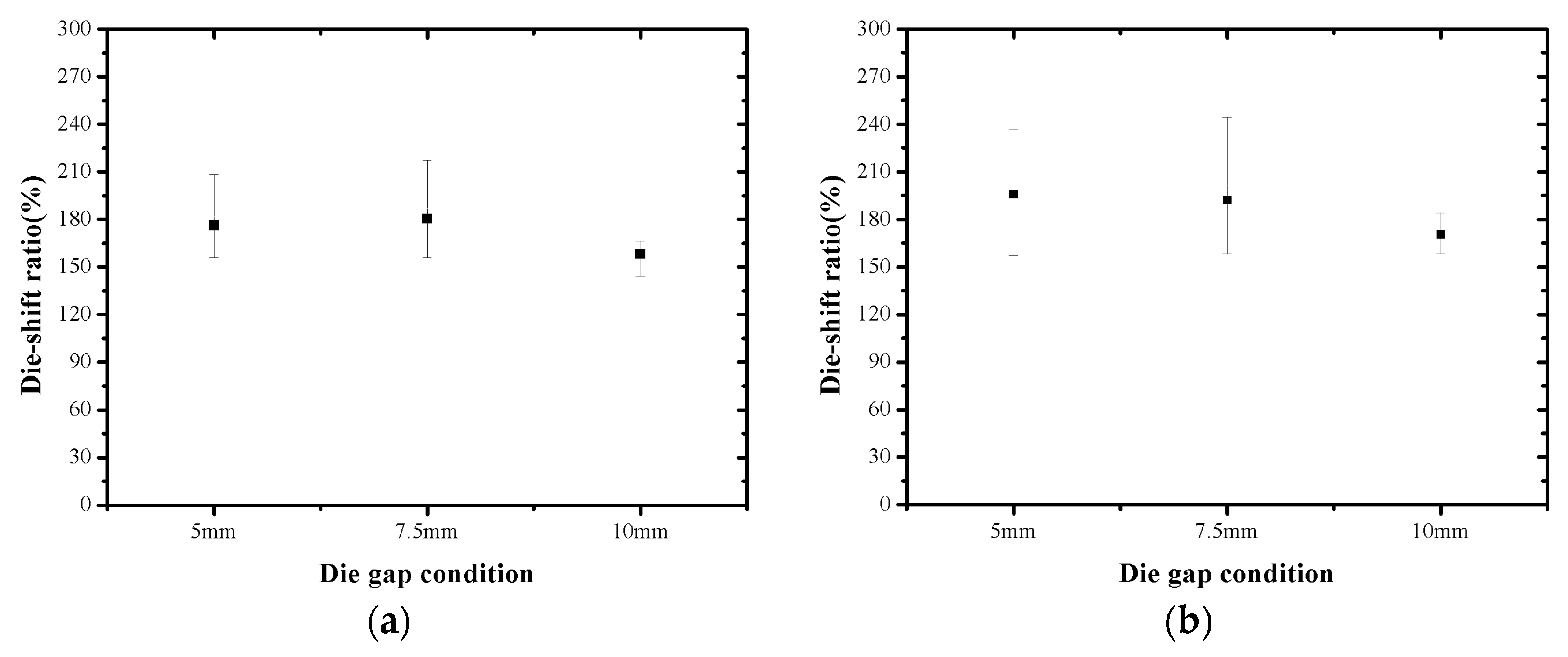
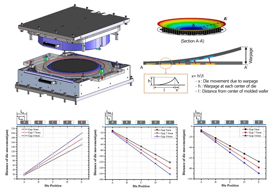
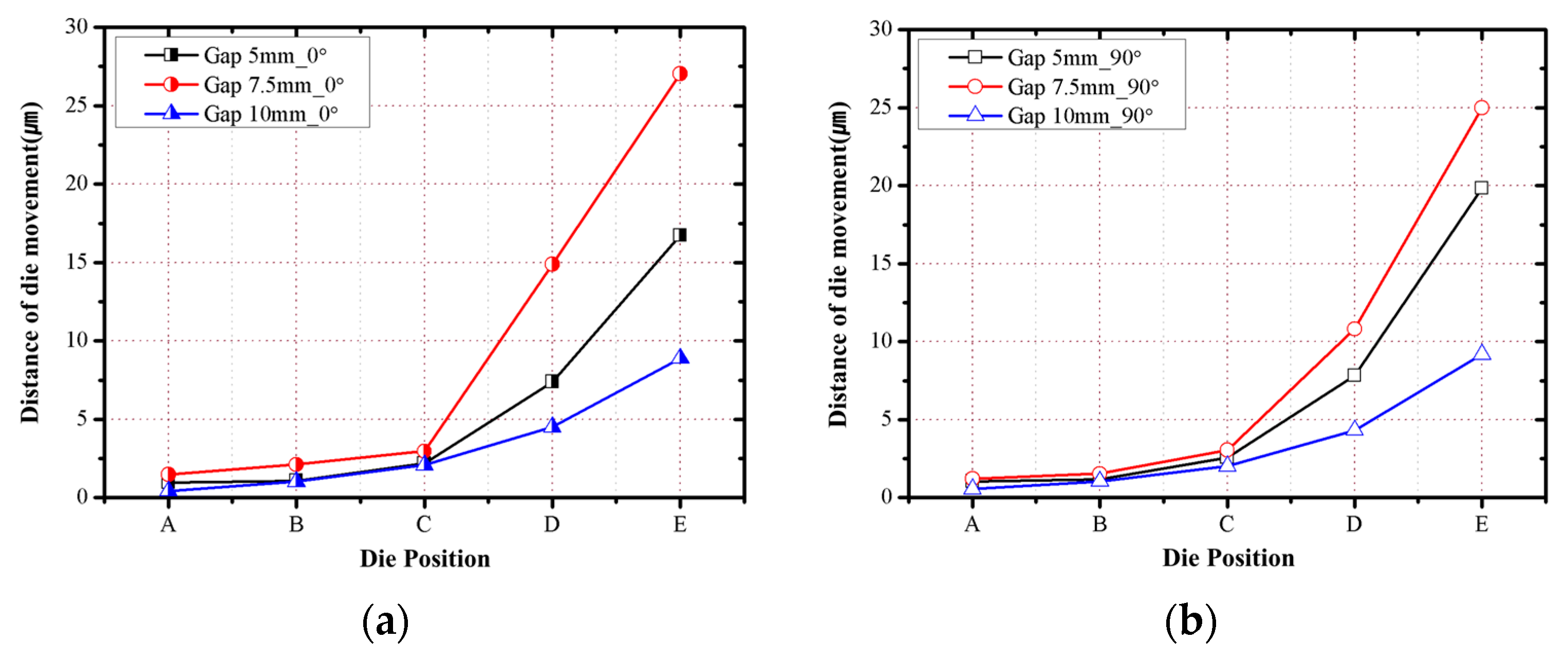
- The die shift increased with the die gap, and the die moved away from the center in the radial direction.
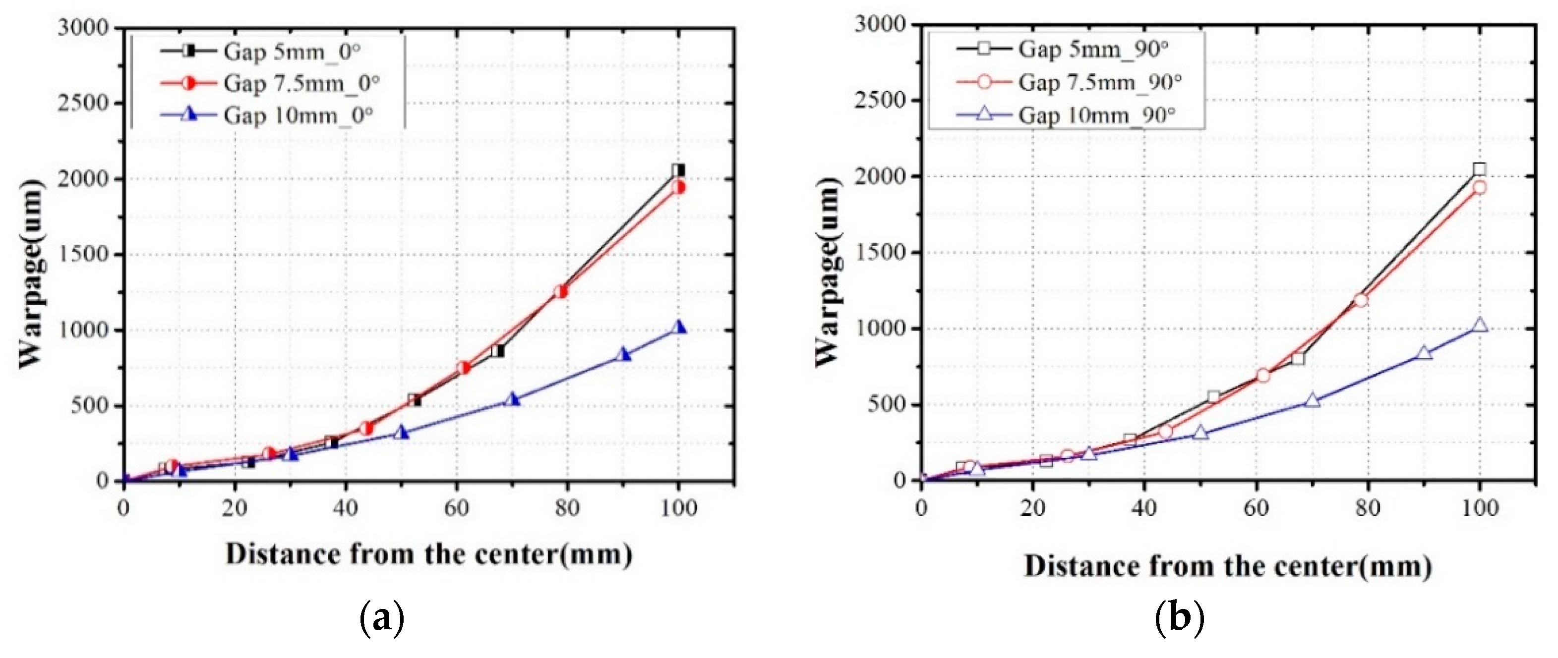
- The warpage increases as the die gap decreases, and it distinctly increases on the outside of the package, where the package die arrangement is uneven.
- The effect of warpage on the die shift increases suddenly for the dies arranged on the outside of a package.
- The die shift caused by EMC flow drag force is evaluated from the data on die movements due to thermal contraction/expansion and warpage.
- The relationship between the die shift and variation in the die gap is determined through regression analysis in order to intuitively predict and reflect the die shift due to flow drag force.
- The die-realignment factor is determined and the position-compensation relationship is derived according to the die position in the package arrangement.
- These results can be used for die realignment by predicting the die shift in advance and compensating for it in the die-realignment process.
Acknowledgments
Author Contributions
Conflicts of Interest
References
- Brunnbauer, M.; Fürgut, E.; Beer, G.; Meyer, T. Embedded wafer level ball grid array (eWLB). In Proceedings of the 8th Electronics Packaging Technology Conference, Singapore, 6–8 December 2006; pp. 1–5.
- Sun, P.; Leung, V.; Yang, D.; Lou, R.; Shi, D.; Chung, T. Development of a new package-on-package (PoP) structure for next-generation portable electronics. In Proceedings of the 60th Electronic Components and Technology Conference (ECTC), Las Vegas, NV, USA, 1–4 June 2010; pp. 1957–1963.
- Dreiza, M.; Kim, J.S.; Smith, L. Joint project for mechanical qualification of next generation high density package-on-package (PoP) with through mold via technology. In Proceedings of the 17th European Microelectronics & Packaging Conference (EMPC), Rimini, Italy, 15–18 June 2009; pp. 1–8.
- Yole Développement. Embedded Wafer-Level-Packages: Fan-out WLP/Chip Embedding in Substrate; Yole Développement: Villeurbanne, France, 2010. [Google Scholar]
- Fillion, R.; Woychik, C.; Zhang, T.; Bitting, D. Embedded chip build-up using fine line interconnect. In Proceedings of the 57th Electronic Components and Technology Conference, Reno, NV, USA, 29 May–1 June 2007; pp. 49–53.
- Ostmann, A.; Manessis, D.; Loeher, T.; Neumann, A.; Reichl, H. Strategies for embedding of active components. In Proceedings of the International Microsystems, Package, Assembly Conference, Taipei, Taiwan, 18–20 October 2006; pp. 1–4.
- Palm, P.; Moisala, J.; Kivikero, A.; Tuominen, R.; lihola, A. Embedding active components inside printed circuit board (PCB) a solution for miniaturization of electronics. In Proceedings of the International Symposium on Advanced Packaging Materials: Processes, Properties and Interfaces, Irvine, CA, USA, 16–18 March 2005; pp. 1–4.
- Yim, M.J.; Strode, R.; Brand, J.; Adimula, R.; Zhang, J.J.; Yoo, C. Ultra thin PoP top package using compression mold: Its warpage control. In Proceedings of the IEEE 61st Electronic Components and Technology Conference (ECTC), Lake Buena Vista, FL, USA, 31 May–3 June 2011; pp. 1141–1146.
- Khong, C.H.; Kumar, A.; Zhang, X.; Sharma, G.; Vempati, S.R.; Vaidyanathan, K.; Lau, J.H.-S.; Kwong, D.L. A novel method to predict die shift during compression molding in embedded wafer level package. In Proceedings of the Electronic Components and Technology Conference, San Diego, CA, USA, 26–29 May 2009; pp. 535–541.
- Ji, L.; Sorono, D.V.; Chai, T.C.; Zhang, X. 3-D numerical and experimental investigations on compression molding in multichip embedded wafer level packaging. IEEE Trans. Compon. Packag. Manuf. Technol. 2012, 3, 678–687. [Google Scholar] [CrossRef]
- Ji, L.; Kim, H.J.; Che, F.; Gao, S.; Pinjala, D. Numerical study of preventing flow-induced die-shift in the compression molding for embedded wafer level packaging. In Proceedings of the Electronics Packaging Technology Conference (EPTC), Singapore, 7–9 December 2011; pp. 406–411.
- Sharma, G.; Kumar, A.; Rao, V.S.; Ho, S.W.; Kripesh, V. Solutions strategies for die shift problem in wafer level compression molding. IEEE Trans. Compon. Packag. Manuf. Technol. 2011, 1, 502–509. [Google Scholar] [CrossRef]
- Ling, H.S.; Bu, L.; Chong, S.C.; Velez, S.D.; Chai, T.; Zhang, X. Comprehensive study on the interactions of multiple die shift mechanisms during wafer level molding of multichip-embedded wafer level packages. IEEE Trans. Compon. Packag. Manuf. Technol. 2014, 4, 1090–1098. [Google Scholar] [CrossRef]
- Bu, L.; Ho, S.; Velez, S.D.; Chai, T.; Zhang, X. Investigation on die shift issues in the 12-in wafer-level compression molding process. IEEE Trans. Compon. Packag. Manuf. Technol. 2013, 3, 1647–1653. [Google Scholar]


| Property | Value | Unit |
|---|---|---|
| Spiral flow | 36 | inch |
| Gelation time | 30 | s |
| Shrinkage (SEMC) | 0.18 | % |
| Glass transition temperature (Tg) | 145 | °C |
| Viscosity | 85.652 | Pa·s |
| Density | 2.00 × 10⁻³ | g/mm3 |
| Material | Value | Unit |
|---|---|---|
| EMC (below Tg 150 °C) | 8 | ppm/°C |
| EMC (above Tg 150 °C) | 49 | ppm/°C |
| Substrate | 17.3 | ppm/°C |
| Die (Silicon) | 2.62 | ppm/°C |
© 2016 by the authors. Licensee MDPI, Basel, Switzerland. This article is an open access article distributed under the terms and conditions of the Creative Commons Attribution (CC-BY) license ( http://creativecommons.org/licenses/by/4.0/).
Share and Cite
Yeon, S.; Park, J.; Lee, H.-J. Compensation Method for Die Shift Caused by Flow Drag Force in Wafer-Level Molding Process. Micromachines 2016, 7, 95. https://doi.org/10.3390/mi7060095
Yeon S, Park J, Lee H-J. Compensation Method for Die Shift Caused by Flow Drag Force in Wafer-Level Molding Process. Micromachines. 2016; 7(6):95. https://doi.org/10.3390/mi7060095
Chicago/Turabian StyleYeon, Simo, Jeanho Park, and Hye-Jin Lee. 2016. "Compensation Method for Die Shift Caused by Flow Drag Force in Wafer-Level Molding Process" Micromachines 7, no. 6: 95. https://doi.org/10.3390/mi7060095
APA StyleYeon, S., Park, J., & Lee, H.-J. (2016). Compensation Method for Die Shift Caused by Flow Drag Force in Wafer-Level Molding Process. Micromachines, 7(6), 95. https://doi.org/10.3390/mi7060095