
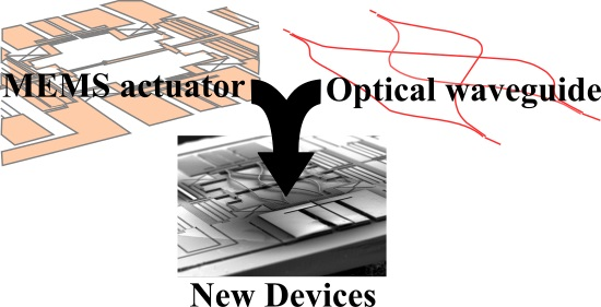
Devices Based on Co-Integrated MEMS Actuators and Optical Waveguide: A Review


Abstract
:
1. Introduction
2. Fabrication Processes for Co-integration of Optical Waveguides and MEMS
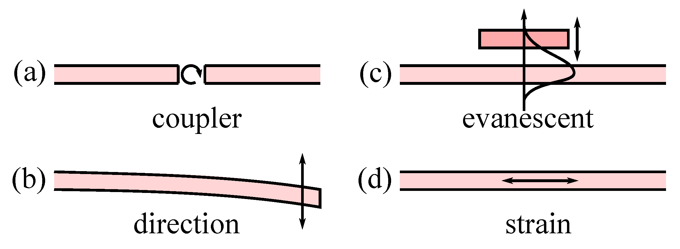
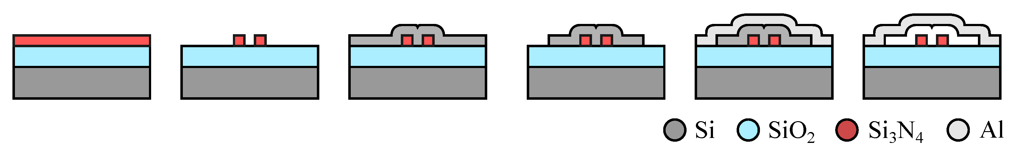
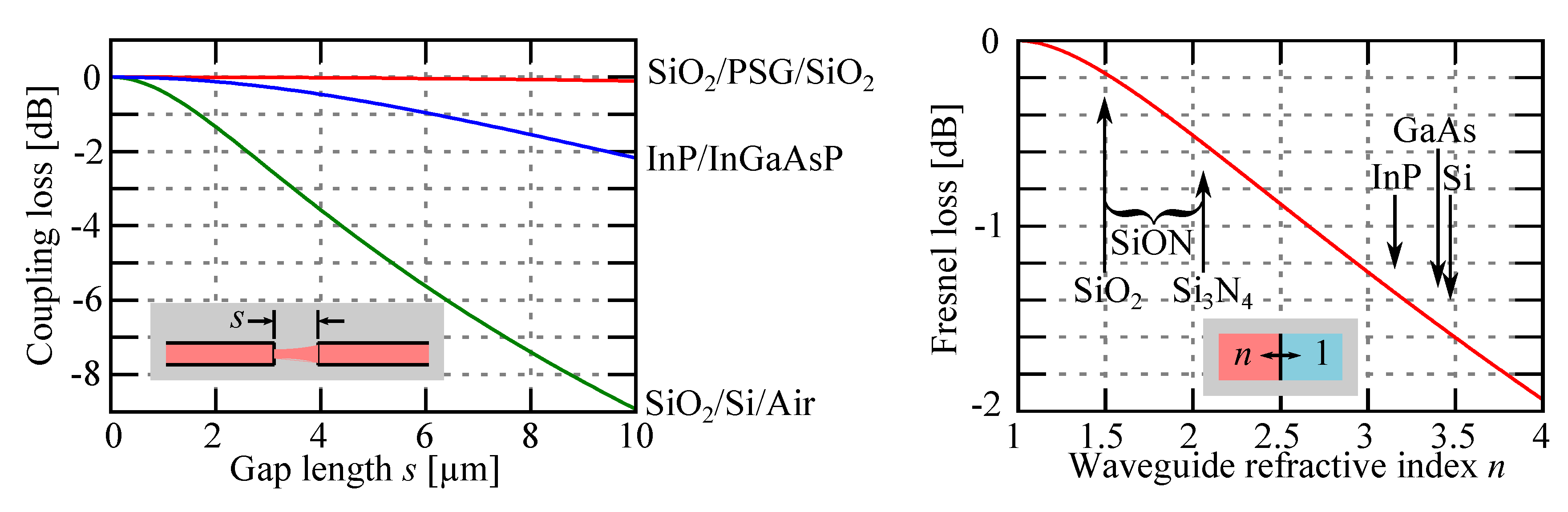
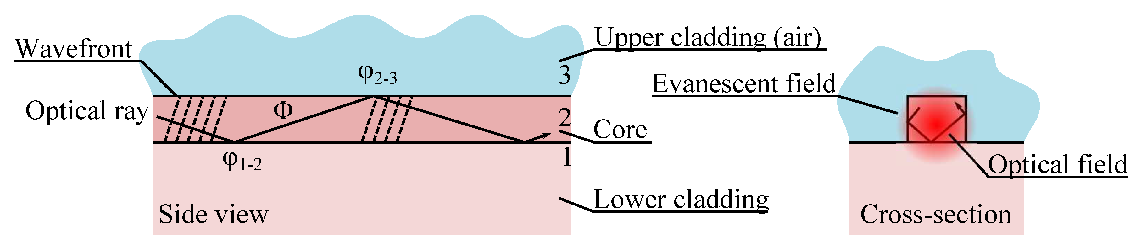
2.1. Waveguide Technology


| Properties | High refractive index contrast | Low refractive index contrast |
|---|---|---|
| Radius of curvature | short | large |
| Propagation loss | high | low |
| Mode field | small | large |
| Coupling with optical fiber | bad | good |
| Evanescent field in air | large | small |
| Waveguide width | λ and sub-λ | several λ |
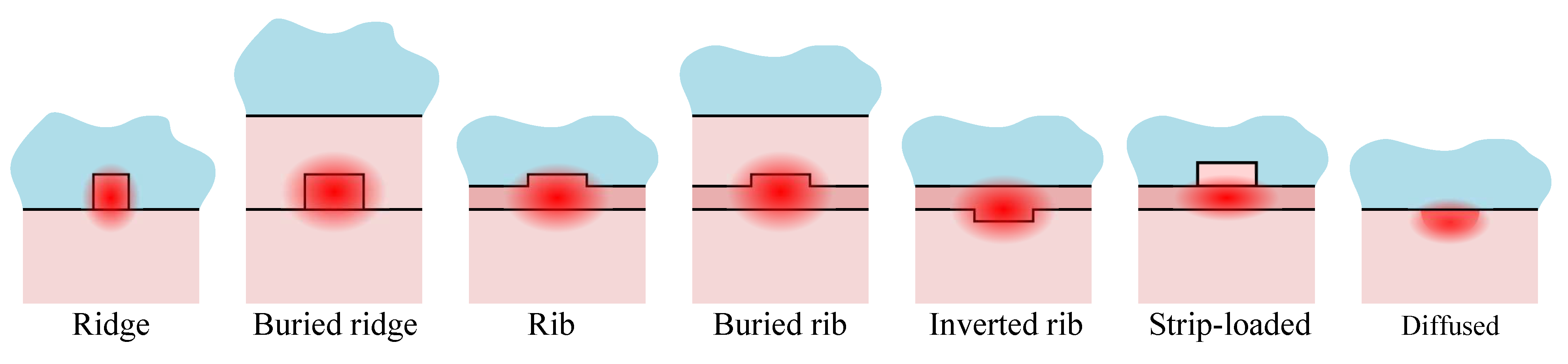
| Materials | Channel | Principle | References |
|---|---|---|---|
| Air/Si/Air | ridge | evanescent | [16,17,18,19,20,21,22,23,24,25,26,27,28,29] |
| coupler | [30] | ||
| direction | [31] | ||
| PhC | evanescent | [32] | |
| slot | evanescent | [33] | |
| GaAs/AlGaAs | ridge | direction | [34] |
| glass/doped glass/Air | diffused | evanescent | [8] |
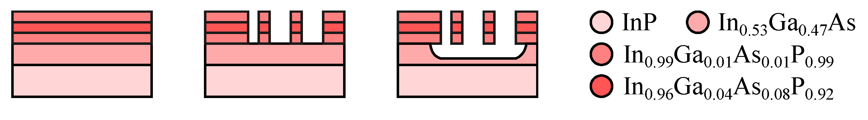
| InP/InGaAsP | ridge | direction | [35,36] |
| evanescent | [37,38,39,40,41,42] | ||
| metal/Air/metal (hollow) | reflection | evanescent | [43] |
| polymer/Air | ridge | coupler | [44,45,46,47] |
| polymer/polymer | ridge | direction | [48] |
| buried ridge | coupler | [49] | |
| SiO2/glass/Air | rib | strain | [4] |
| SiO2/Au | plasmon | evanescent | [50] |
| SiO2/Al2O3/SiO2 | ridge | direction | [51] |
| SiO2/BK7/SiO2 | strip-loaded | strain | [52] |
| SiO2/PS/Air | inverted rib | strain | [53] |
| SiO2/PSG/Air | rib | evanescent | [54] |
| SiO2/PSG/SiO2 | buried rib | direction | [55,56,57,58,59,60,61,62] |
| coupler | [63,64,65] | ||
| buried ridge | coupler | [28] | |
| SiO2/Si/Air | rib | coupler | [26,27] |
| SiO2/SiON/Air | rib | evanescent | [66,67,68,69] |
| rib | strain | [70] | |
| rib ARROW | strain | [71] | |
| ridge | evanescent | [72,73,74,75] | |
| SiO2/SiON/SiO2 | buried ridge | coupler | [76] |
| strip loaded | strain | [77,78,79] | |
| rib | evanescent | [80] | |
| inverse rib | direction | [6] | |
| buried rib | direction | [81] | |
| SiO2/TiO2/Air | planar | evanescent | [7,82,83,84] |
2.2. MEMS Actuator and Waveguide Co-integration


| Materials | Principle | Co-integration | References |
|---|---|---|---|
| Au | gap-closing | monolithic | [50] |
| fluid | thermal | hybrid | [63,64] |
| electrostatic | hybrid | [65] | |
| GaAs/AlGaAs | comb-drive | monolithic | [34] |
| glass | (sensing) | hybrid | [7,82] |
| InGaAsP | gap-closing | monolithic | [35,36,39] |
| light | monolithic | [40] | |
| (sensing) | monolithic | [41] | |
| InP | gap-closing | monolithic | [37] |
| metal | gap-closing | hybrid | [5,54] |
| stacked | [72,74,75] | ||
| Ni/Fe | magnetic | hybrid | [55,56] |
| polymer/metal | gap-closing | monolithic | [8] |
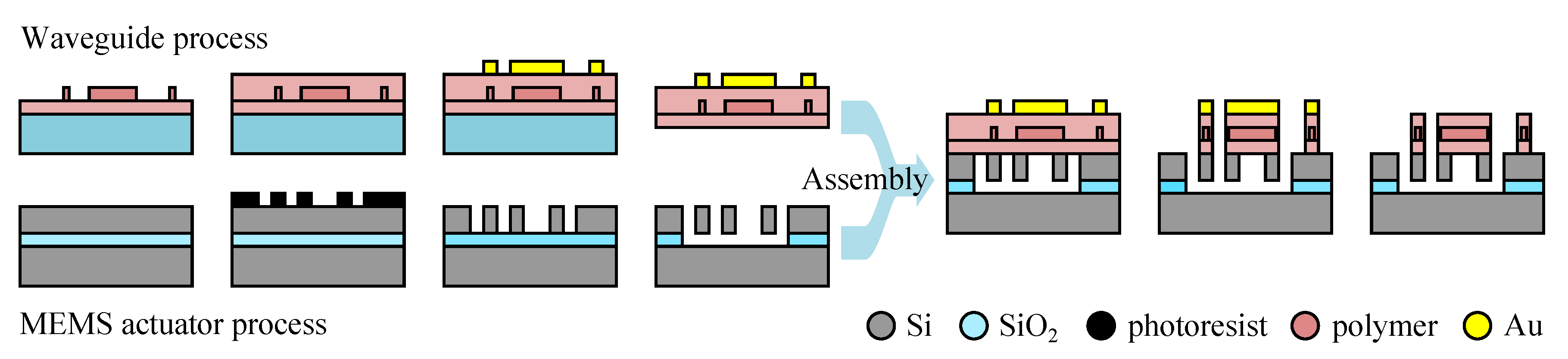
| poly-Si | gap-closing | hybrid | [28] |
| Si | gap-closing | hybrid | [67,68,69,73,89] |
| monolithic | [20,21] | ||
| (sensing) | monolithic | [30] | |
| stacked | [4,52,53,70,71,77,78,79] | ||
| SiON | gap-closing | hybrid | [66,83] |
| monolithic | [57,58,61,62] | ||
| (sensing) | hybrid | [84] | |
| monolithic | [6,51,59,60,81] | ||
| SOI | comb-drive | hybrid | [49] |
| monolithic | [19,22,24,25,26,27,31,32,48] | ||
| stacked | [76] | ||
| gap-closing | monolithic | [16,17,23,29,43] | |
| (sensing) | monolithic | [33] |
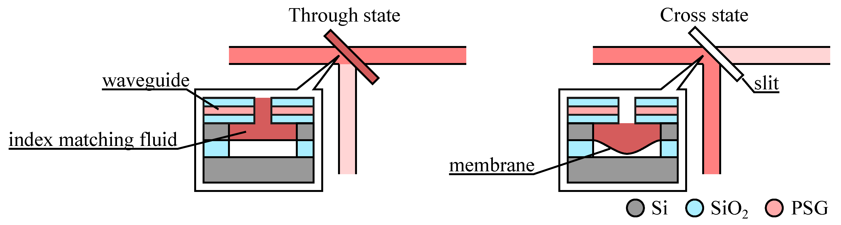
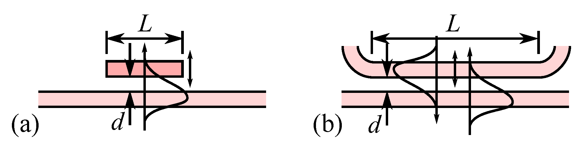
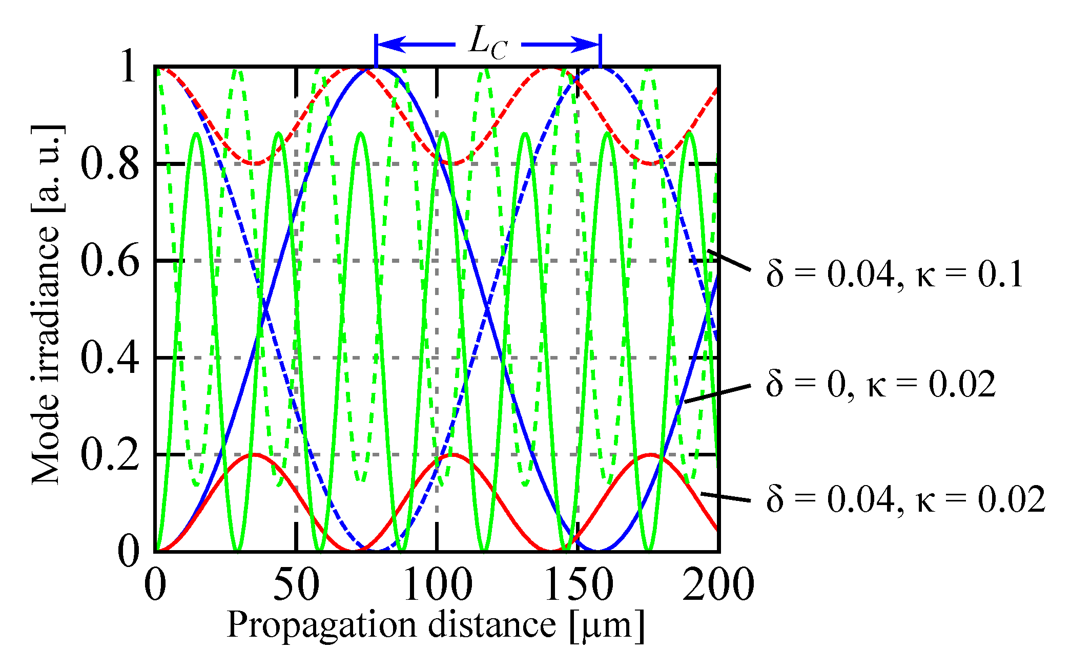
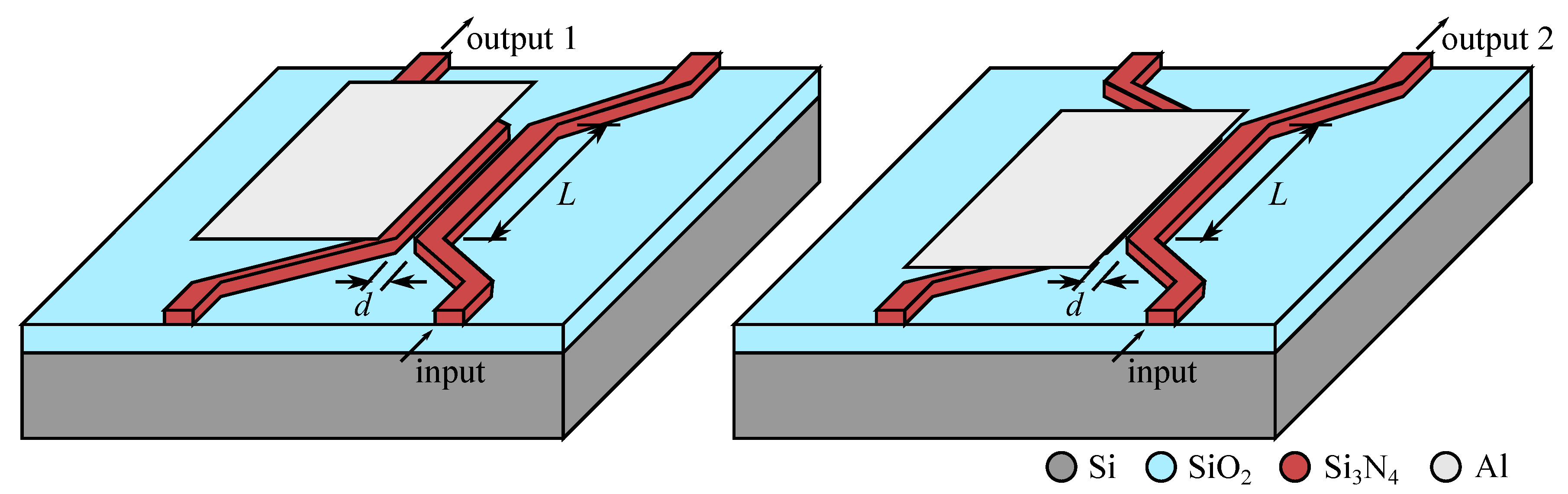
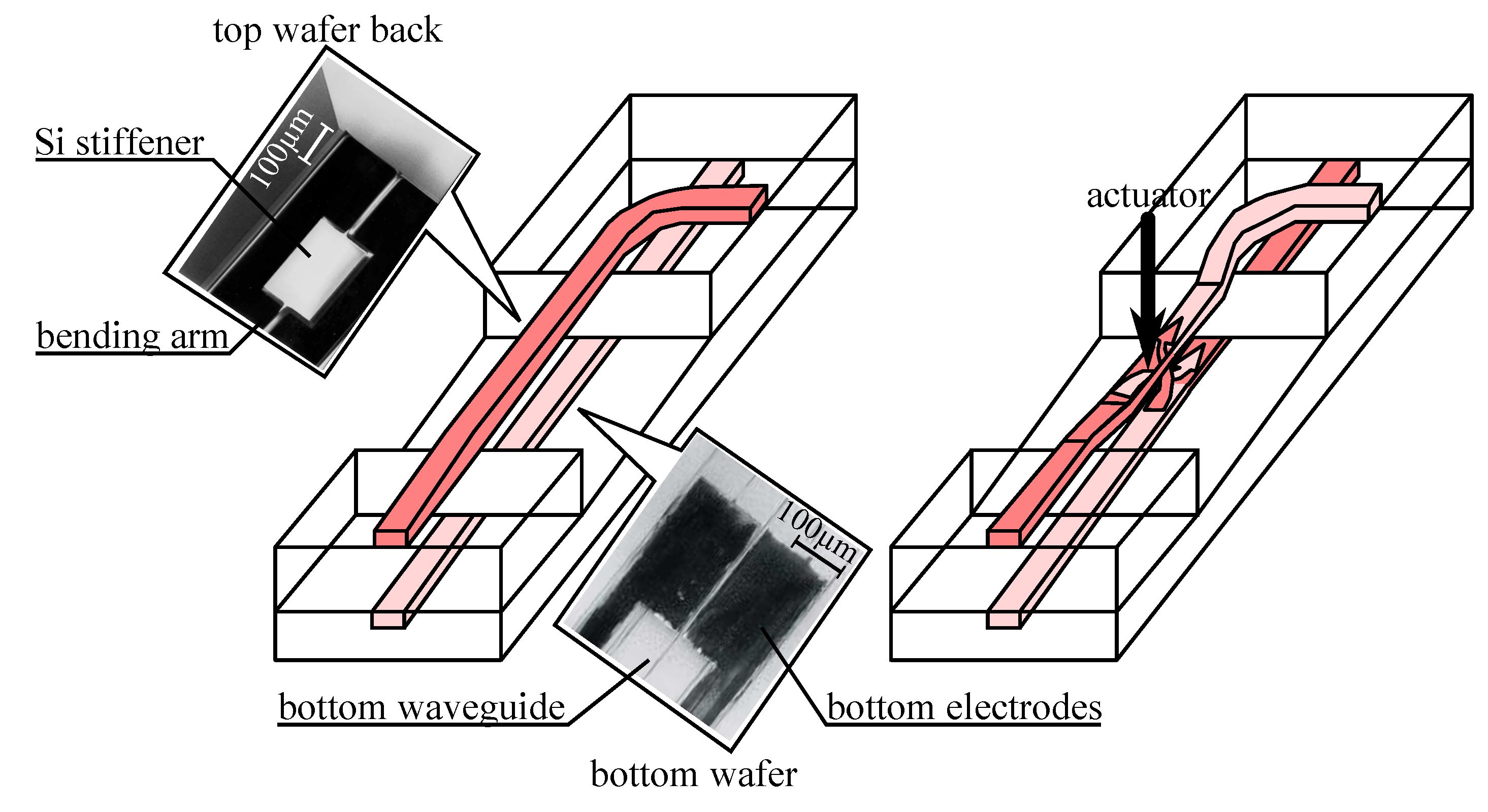
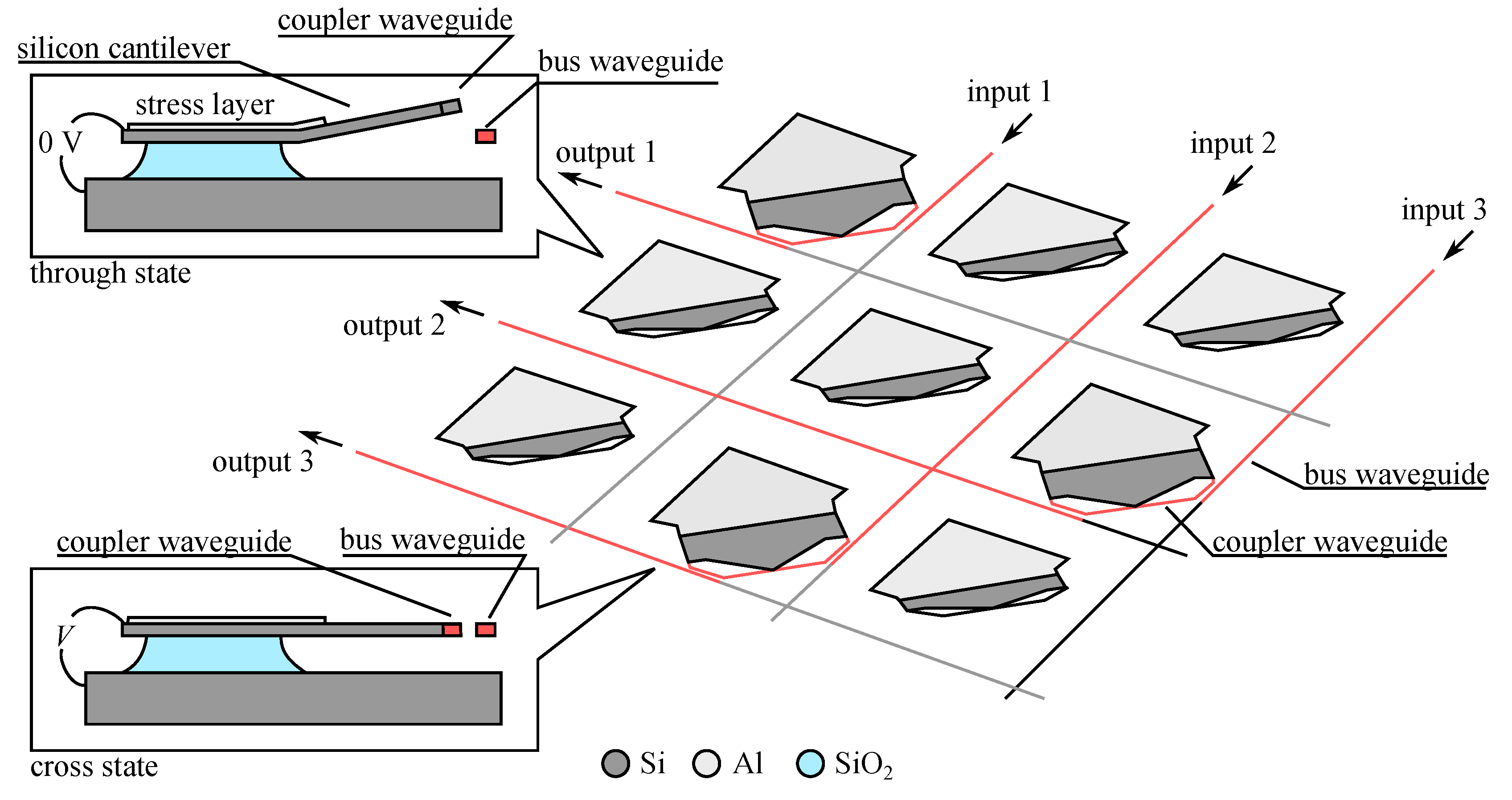
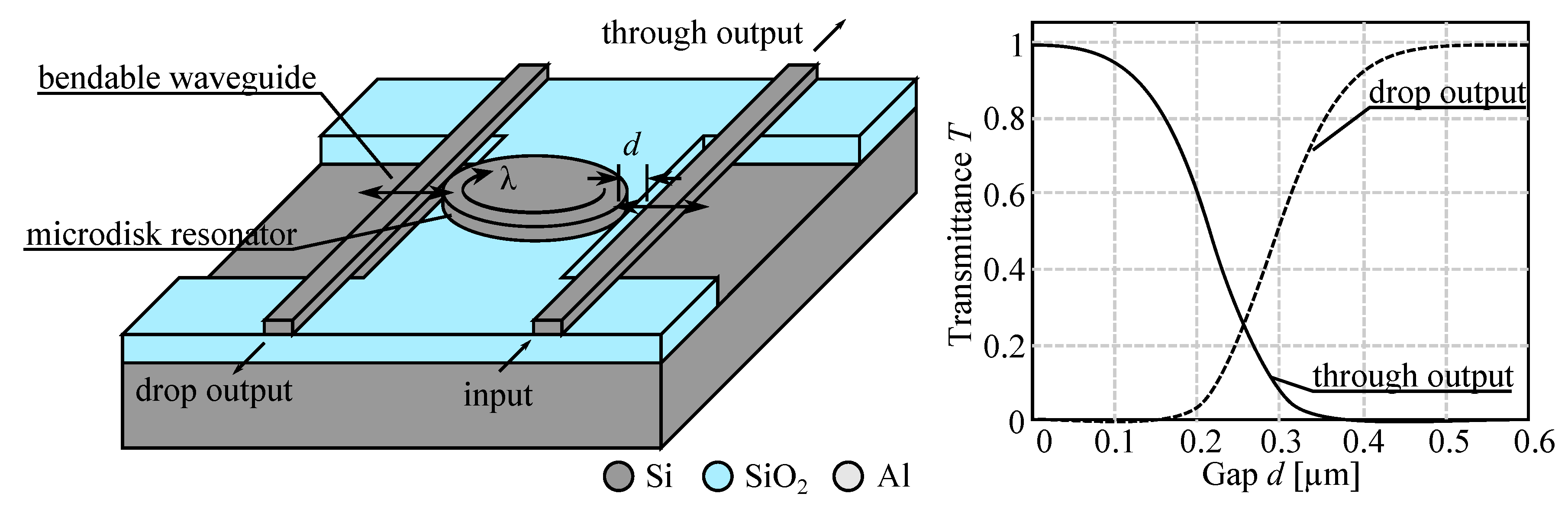
3. Devices Based on Coupling Between Fixed Waveguides
3.1. Design Consideration
3.2. Principle Application

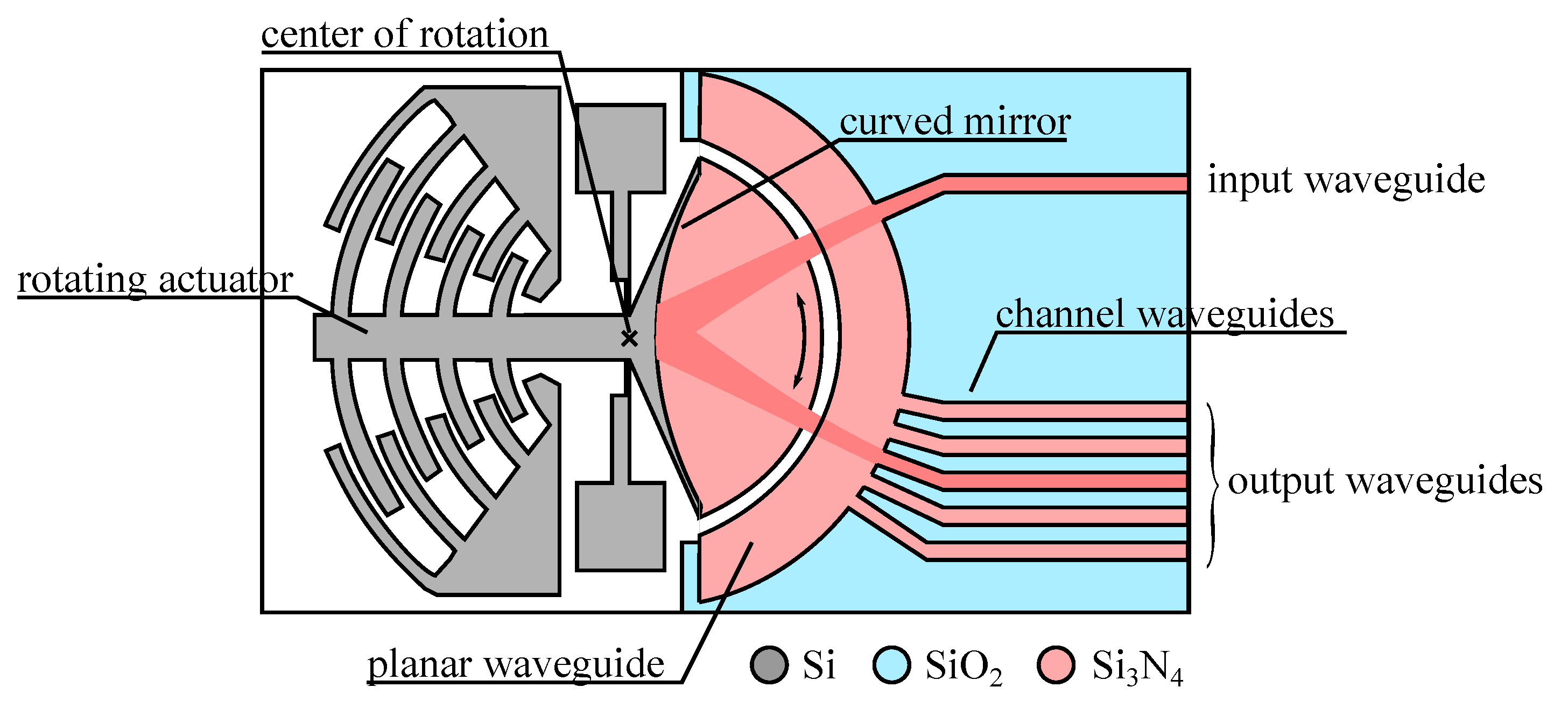


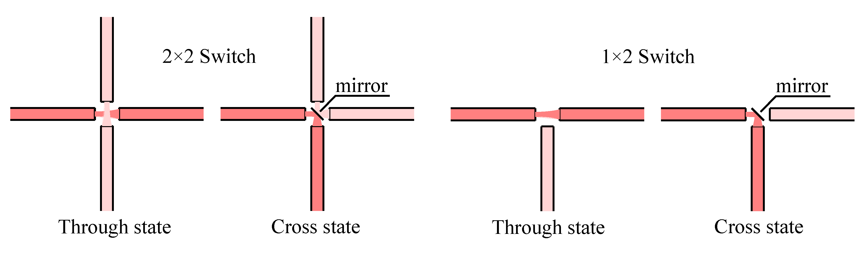
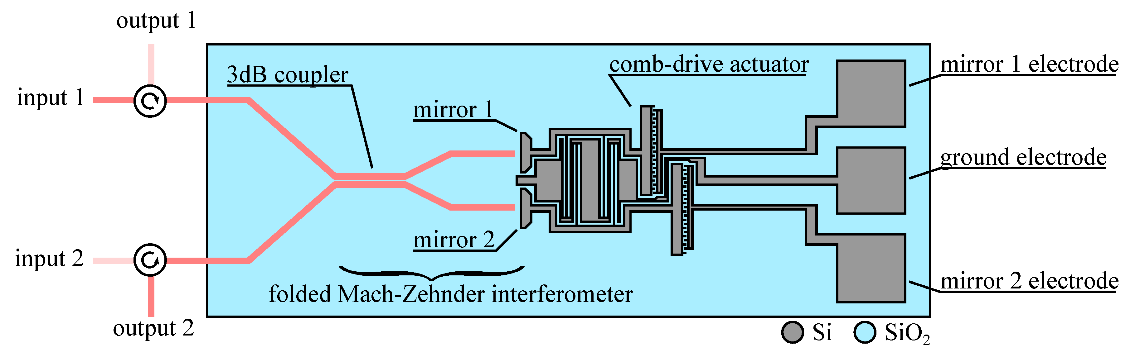
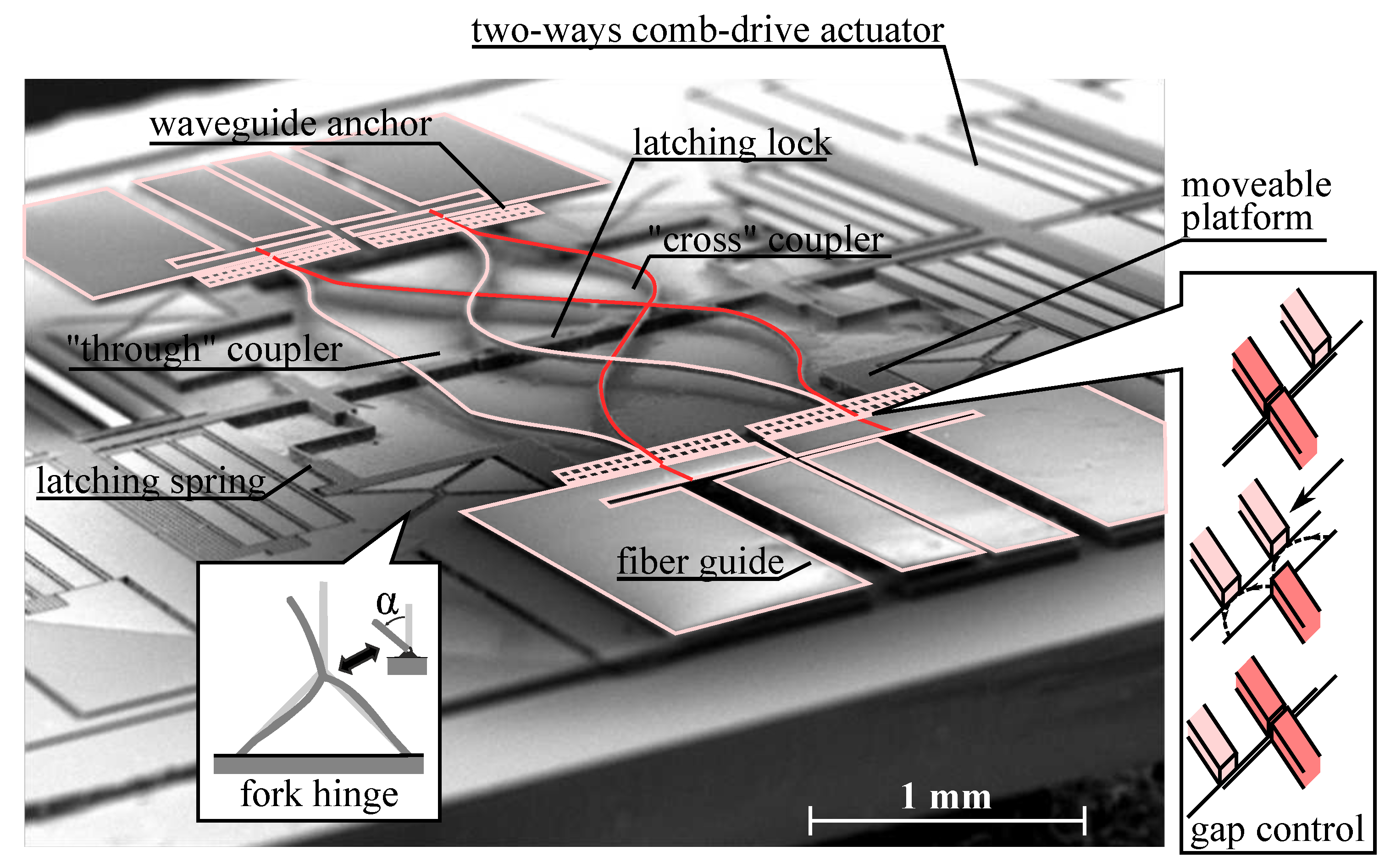
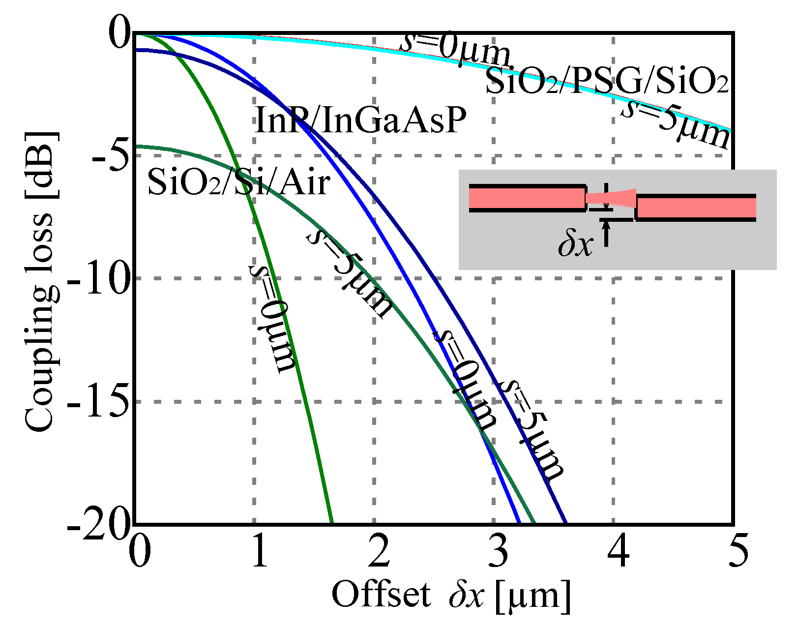
4. Devices Based on Modification of Waveguide Direction
4.1. Design Consideration

4.2. Principle Application

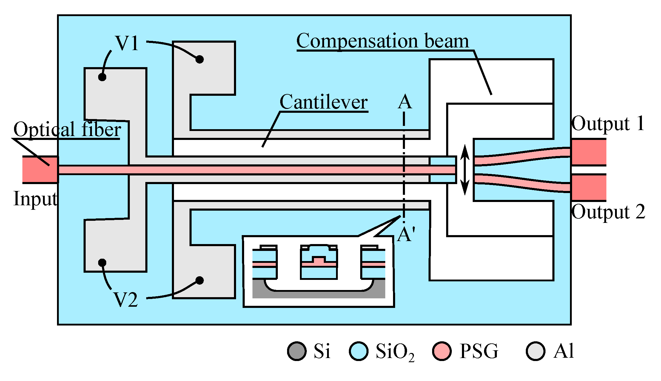
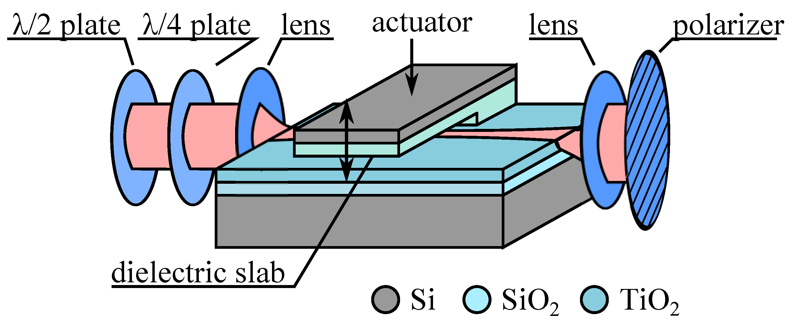
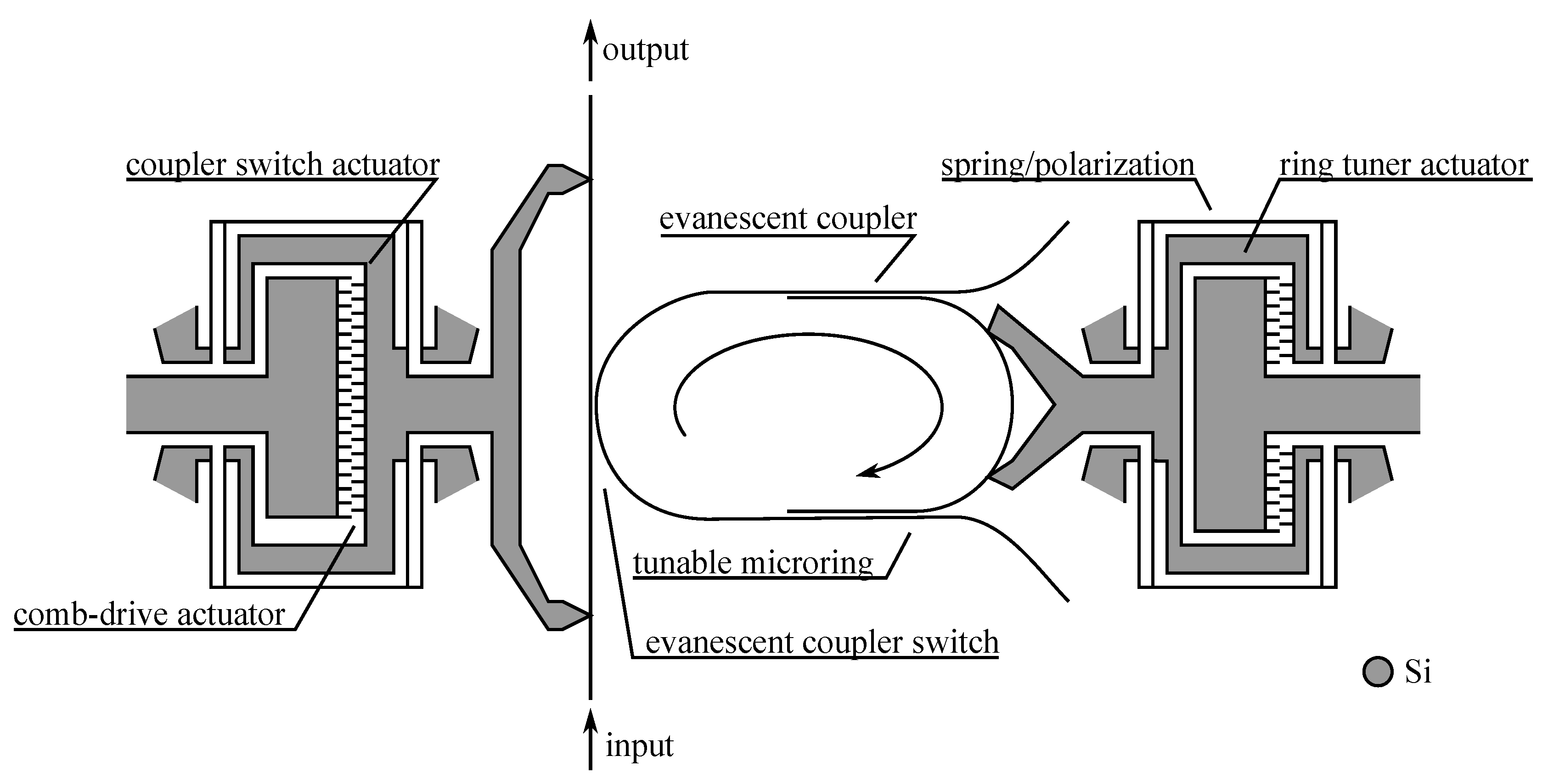
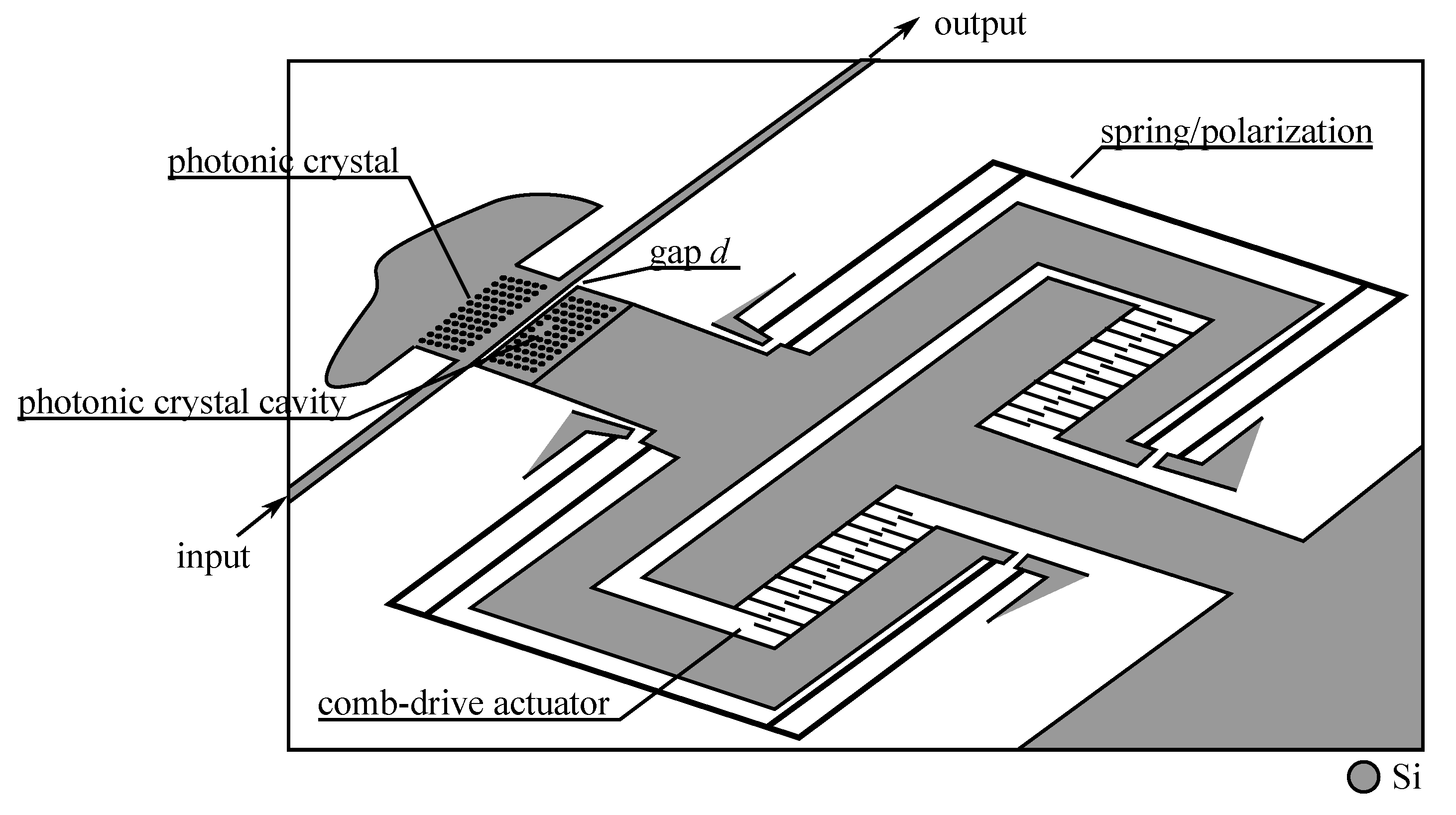
5. Devices Based on Interaction with the Waveguide Evanescent Field
5.1. Design Consideration


5.2. Principle Application


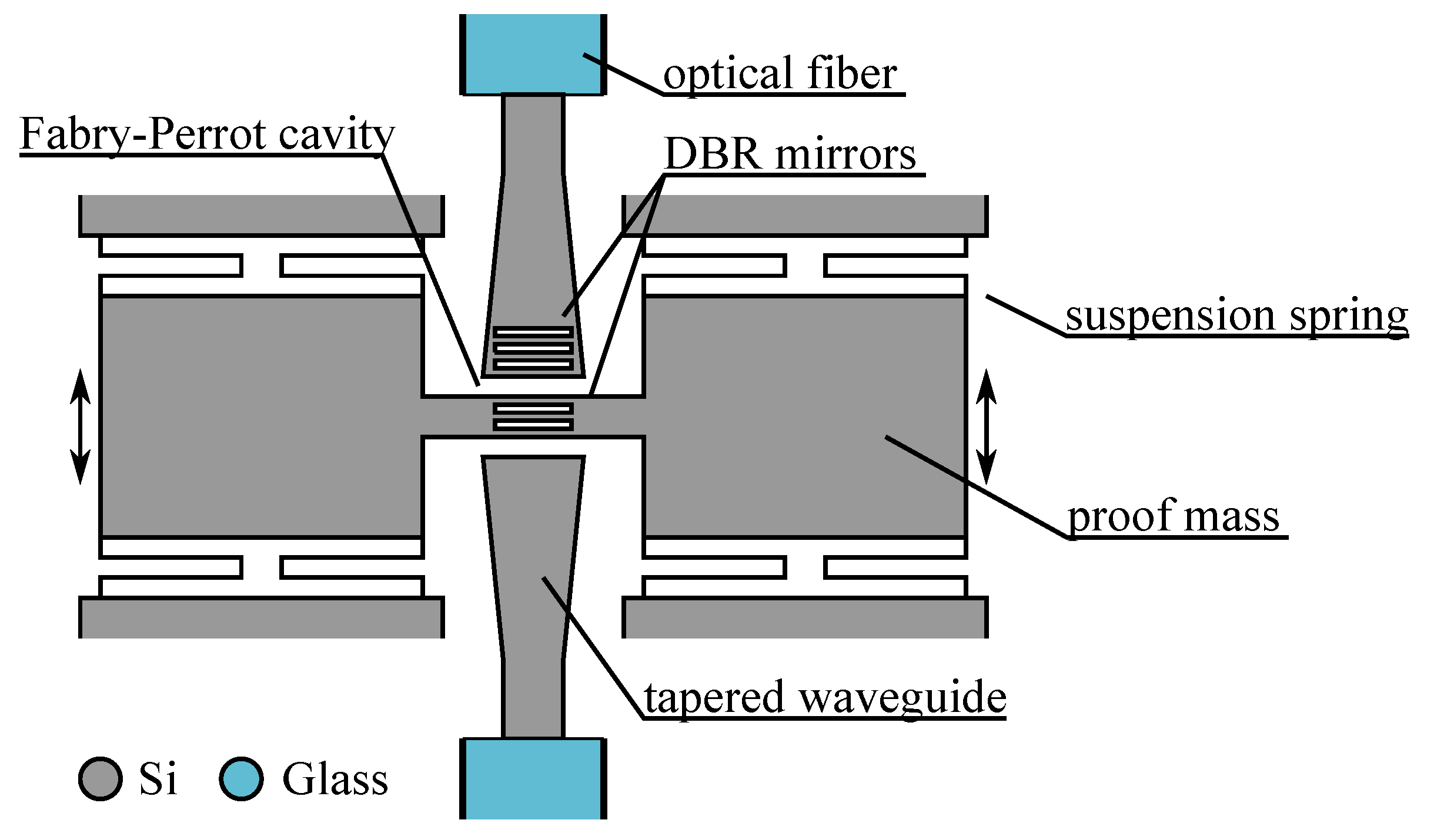
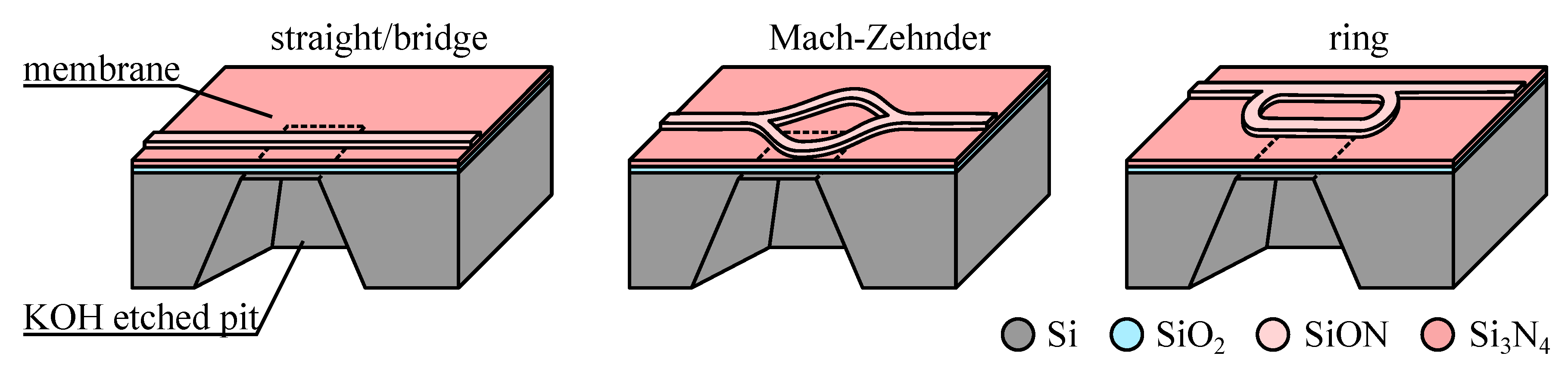
6. Devices Based on Change of the Waveguide Strain
6.1. Design Consideration
6.2. Principle Application

7. Conclusions
Acknowledgments
Conflicts of Interest
References
- Miller, S. Integrated optics: An introduction. Bell Syst. Tech. J. 1969, 48, 2059. [Google Scholar] [CrossRef]
- Nathanson, H.; Wickstrom, R. A resonant-gate silicon surface transistor with high-Q bandpass properties. Appl. Phys. Lett. 1965, 7, 84–86. [Google Scholar] [CrossRef]
- Maluf, N. Foreword. In An Introduction to Microelectromechanical Systems Engineering; Artech House: Norwood, MA, USA, 1999; p. xiii. [Google Scholar]
- Ohkawa, M.; Izutsu, M.; Sueta, T. Integrated optic pressure sensor on silicon substrate. Appl. Opt. 1989, 28, 5153–5157. [Google Scholar] [CrossRef] [PubMed]
- Hogari, K.; Matsumoto, T. Electrostatically driven micromechanical 2X2 optical switch. Appl. Opt. 1991, 30, 1253–1257. [Google Scholar] [CrossRef] [PubMed]
- Bezzaoui, H.; Voges, E. Integrated optics combined with micromechanics on silicon. Sens. Actuators A Phys. 1991, 29, 219–223. [Google Scholar] [CrossRef]
- Lukosz, W.; Pliska, P. Integrated optical interferometer as a light modulator and microphone. Sens. Actuators A Phys. 1991, 26, 337–340. [Google Scholar] [CrossRef]
- Kim, Y.; Allen, M.; Hartman, N. Micromechanically based integrated optic modulators and switches. Proc. SPIE 1992, 1793, 183–189. [Google Scholar]
- Marxer, C.; Thio, C.; Grétillat, M.A.; de Rooij, N.; Bättig, R.; Anthamatten, O.; Valk, B.; Vogel, P. Vertical Mirrors Fabricated by Deep Reactive Ion Etching for Fiber-Optic Switching Applications. J. Microelectromech. Syst. 1997, 6, 277–285. [Google Scholar] [CrossRef]
- Toshiyoshi, H.; Fujita, H. Electrostatic Micro Torsion Mirrors for an Optical Switch Matrix. J. Microelectromech. Syst. 1996, 5, 231–237. [Google Scholar] [CrossRef]
- Roussey, M.; Bernal, M.P.; Courjal, N.; Van Labeke, D.; Baida, F.I.; Salut, R. Electro-optic effect exaltation on lithium niobate photonic crystals due to slow photons. Appl. Phys. Lett. 2006, 89, 241110. [Google Scholar] [CrossRef]
- Tabib-Azar, M.; Beheim, G. Modern trends in microstructures and integrated optics for communication, sensing, and actuation. Opt. Eng. 1997, 36, 1307–1318. [Google Scholar]
- Solgaard, O.; Godil, A.A.; Howe, R.T.; Lee, L.P.; Peter, Y.A.; Zappe, H. Optical MEMS: From Micromirrors to Complex Systems. J. Microelectromech. Syst. 2014, 23, 517–538. [Google Scholar] [CrossRef]
- Marcuse, D. Light Transmission Optics; Van Nostrand Reinhold: New York, NY, USA, 1972. [Google Scholar]
- Duguay, M.A.; Kokubun, Y.; Koch, T.L.; Pfeiffer, L. Antiresonant reflecting optical waveguides in SiO2-Si multilayer structures. Appl. Phys. Lett. 1986, 49, 13–15. [Google Scholar] [CrossRef]
- Lee, M.C.; Wu, M. MEMS-actuated microdisk resonators with variable power coupling ratios. IEEE Photon. Technol. Lett. 2005, 17, 1034–1036. [Google Scholar] [CrossRef]
- Lee, M.C.M.; Wu, M.C. Tunable coupling regimes of silicon microdisk resonators using MEMS actuators. Opt. Express 2006, 14, 4703–4712. [Google Scholar] [CrossRef] [PubMed]
- Nawrocka, M.S.; Liu, T.; Wang, X.; Panepucci, R.R. Tunable silicon microring resonator with wide free spectral range. Appl. Phys. Lett. 2006, 89, 071110. [Google Scholar] [CrossRef]
- Takahashi, K.; Kanamori, Y.; Kokubun, Y.; Hane, K. A wavelength-selective add-drop switch using silicon microring resonator with a submicron-comb electrostatic actuator. Opt. Express 2008, 16, 14421. [Google Scholar] [CrossRef] [PubMed]
- Yao, J.; Leuenberger, D.; Lee, M.C.M.; Wu, M. Silicon Microtoroidal Resonators With Integrated MEMS Tunable Coupler. IEEE J. Sel. Top. Quantum Electron. 2007, 13, 202–208. [Google Scholar] [CrossRef]
- Yao, J.; Wu, M.C. Bandwidth-tunable add-drop filters based on micro-electro-mechanical-system actuated silicon microtoroidal resonators. Opt. Lett. 2009, 34, 2557. [Google Scholar] [CrossRef] [PubMed]
- Akihama, Y.; Kanamori, Y.; Hane, K. Ultra-small silicon waveguide coupler switch using gap-variable mechanism. Opt. Express 2011, 19, 23658. [Google Scholar] [CrossRef] [PubMed]
- Chatterjee, R.; Wong, C.W. Nanomechanical Proximity Perturbation for Switching in Silicon-Based Directional Couplers for High-Density Photonic Integrated Circuits. J. Microelectromech. Syst. 2010, 19, 657–662. [Google Scholar] [CrossRef]
- Ikeda, T.; Takahashi, K.; Kanamori, Y.; Hane, K. Phase-shifter using submicron silicon waveguide couplers with ultra-small electro-mechanical actuator. Opt. Express 2010, 18, 7031. [Google Scholar] [CrossRef] [PubMed]
- Ikeda, T.; Kanamori, Y.; Hane, K. Si photonic nano-wire tunble micro-ring resonator composed of triply-liked variable couplers. In Proceedings of 2012 IEEE 25th International Conference on Micro Electro Mechanical Systems (MEMS 2012), Paris, France, 29 January–2 Febuary 2012.
- Baumann, F.; Chan, H.; Fuchs, D.; Stuart, H. Monolithic waveguide/MEMS switch. U.S. Patent 7155083.
- Fuchs, D.; Chan, H.; Stuart, H.; Baumann, F.; Greywall, D.; Simon, M.; Wong-Foy, A. Monolithic integration of MEMS-based phase shifters and optical waveguides in silicon-on-insulator. Electron. Lett. 2004, 40, 142. [Google Scholar] [CrossRef]
- Fuchs, D.; Doerr, C.; Aksyuk, V.; Simon, M.; Stulz, L.; Chandrasekhar, S.; Buhl, L.; Cappuzzo, M.; Gomez, L.; Wong-Foy, A.; et al. A Hybrid MEMS-Waveguide Wavelength Selective Cross Connect. IEEE Photon. Technol. Lett. 2004, 16, 99–101. [Google Scholar] [CrossRef]
- Han, S.; Seok, T.J.; Quack, N.; Yoo, B.W.; Wu, M.C. Large-scale silicon photonic switches with movable directional couplers. Optica 2015, 2, 370–375. [Google Scholar] [CrossRef]
- Zandi, K.; Belanger, J.A.; Peter, Y.A. Design and Demonstration of an In-Plane Silicon-on-Insulator Optical MEMS Fabry-Pérot-Based Accelerometer Integrated With Channel Waveguides. J. Microelectromech. Syst. 2012, 21, 1464–1470. [Google Scholar] [CrossRef]
- Bulgan, E.; Kanamori, Y.; Hane, K. Submicron silicon waveguide optical switch driven by microelectromechanical actuator. Appl. Phys. Lett. 2008, 92, 101110. [Google Scholar] [CrossRef]
- Kanamori, Y.; Takahashi, K.; Hane, K. An ultrasmall wavelength-selective channel drop switch using a nanomechanical photonic crystal nanocavity. Appl. Phys. Lett. 2009, 95, 171911. [Google Scholar] [CrossRef]
- Li, M.; Pernice, W.H.P.; Tang, H.X. Ultrahigh-frequency nano-optomechanical resonators in slot waveguide ring cavities. Appl. Phys. Lett. 2010, 97, 183110. [Google Scholar] [CrossRef]
- Bakke, T.; Tigges, C.; Lean, J.; Sullivan, T.; Spahn, O. Planar microoptomechanical waveguide switches. IEEE J. Sel. Top. Quantum Electron. 2002, 8, 64–72. [Google Scholar] [CrossRef]
- Pruessner, M.; Kelly, D.; Datta, M.; Lim, H.; Maboudian, R.; Ghodssi, R. Design and fabrication of an InP-based moving waveguide 1 × 2 optical MEMS switch. In Proceedings of 2003 International Semiconductor Device Research Symposium, Washington, DC, USA, 10–12 December 2003; pp. 280–281.
- Pruessner, M.W.; Siwak, N.; Amarnath, K.; Kanakaraju, S.; Chuang, W.H.; Ghodssi, R. End-coupled optical waveguide MEMS devices in the indium phosphide material system. J. Micromech. Microeng. 2006, 16, 832–842. [Google Scholar] [CrossRef]
- Podoliak, N.; Ng, W.H.; Liu, H.; Kenyon, A.J.; Stewart, W.; Horak, P. MEMS actuation for a continuously tunable optical buffer. In Proceedings of 2014 International Conference on Optical MEMS and Nanophotonics, Glasgow, UK, 17–21 August 2014; pp. 103–104.
- Kelly, D.; Pruessner, M.; Amarnath, K.; Datta, M.; Kanakaraju, S.; Calhoun, L.; Ghodssi, R. Monolithic Suspended Optical Waveguides for InP MEMS. IEEE Photon. Technol. Lett. 2004, 16, 1298–1300. [Google Scholar] [CrossRef]
- Pruessner, M.; Amarnath, K.; Datta, M.; Kelly, D.; Kanakaraju, S.; Ho, P.T.; Ghodssi, R. InP-based optical waveguide MEMS switches with evanescent coupling mechanism. J. Microelectromech. Syst. 2005, 14, 1070–1081. [Google Scholar] [CrossRef]
- Pruessner, M.W.; Stievater, T.H.; Khurgin, J.B.; Rabinovich, W.S. Integrated waveguide-DBR microcavity opto-mechanical system. Opt. Express 2011, 19, 21904. [Google Scholar] [CrossRef] [PubMed]
- Pruessner, M.; Park, D.; Stievater, T.; Kozak, D.; Rabinovich, W. An Optomechanical Transducer Platform for Evanescent Field Displacement Sensing. IEEE Sens. J. 2014, 14, 3473–3481. [Google Scholar] [CrossRef]
- Siwak, N.P.; Fan, X.Z.; Ghodssi, R. Fabrication challenges for indium phosphide microsystems. J. Micromech. Microeng. 2015, 25, 043001. [Google Scholar] [CrossRef]
- Guerre, R.; Fahrni, F.; Renaud, P. Fast 10-μs Microelectromechanical Optical Switch Inside a Planar Hollow Waveguide (PHW). J. Lightwave Technol. 2006, 24, 1486. [Google Scholar] [CrossRef]
- Brown, K.S.; Taylor, B.J.; Dawson, J.M.; Hornak, L.A. Polymer waveguide cointegration with microelectromechanical systems (MEMS) for integrated optical metrology. Proc. SPIE 1998, 3276, 112–122. [Google Scholar]
- Dickey, F.M.; Holswade, S.C.; Hornak, L.A.; Brown, K.S. Optical methods for micromachine monitoring and feedback. Sens. Actuators A Phys. 1999, 78, 220–235. [Google Scholar] [CrossRef]
- Hornak, L.; Famouri, P.; Dawson, J.; Wang, L.; Ghaffarian, R. MOEMS Integrated Optical Monitoring. Proc. SPIE 2001, 4561, 221–230. [Google Scholar]
- Dawson, J.; Wang, L.; McCormick, W.; Rittenhouse, S.; Famouri, P.; Hornak, L. Integrated Optical Monitoring of MEMS for Closed-Loop Control. Proc. SPIE 2003, 4983, 34. [Google Scholar]
- Bakke, T.; Tigges, C.; Sullivan, C. 1 × 2 MOEMS switch based on silicon-on-insulator and polymeric waveguides. Electron. Lett. 2002, 38, 177–178. [Google Scholar] [CrossRef]
- Liu, H.B.; Chollet, F. Moving Polymer Waveguides and Latching Actuator for 2 × 2 MEMS Optical Switch. J. Microelectromech. Syst. 2009, 18, 715–724. [Google Scholar]
- Dennis, B.S.; Haftel, M.I.; Czaplewski, D.A.; Lopez, D.; Blumberg, G.; Aksyuk, V.A. Compact nanomechanical plasmonic phase modulators. Nat. Photon. 2015, 9, 563–576. [Google Scholar] [CrossRef]
- Wu, S.; Frankena, H.J. Integrated optical sensors using micromechanical bridges and cantilevers. Proc. SPIE 1993, 1793, 83. [Google Scholar]
- Saito, N.; Miura, Y.; Oshima, T.; Ohkawa, M.; Sato, T. Experimental study of sensitivity dependences on waveguide position and diaphragm thickness in silicon-based guided-wave optical accelerometer. Opt. Eng. 2013, 52, 024604. [Google Scholar] [CrossRef]
- Ohkawa, M.; Sato, T. Scale-reduction rule without drop in the sensitivity of a silicon-based guided-wave optical pressure sensor using a micromachined diaphragm. Opt. Eng. 2012, 51, 014401. [Google Scholar] [CrossRef]
- Boysel, R.M.; McDonald, T.G.; Magel, G.A.; Smith, G.C.; Leonard, J.L., Jr.; Tabib-Azar, M.; Polla, D.L. Integration of deformable mirror devices with optical fibers and waveguides. Proc. SPIE 1993, 1793, 34–39. [Google Scholar]
- Kobayashi, D.; Okano, H.; Horie, M.; Otsuki, H.; Sato, K.; Horino, M. PLC-based micromechanical optical switch with magnetic drive. In Proceedings of 1997 IEEE/LEOS International Conference on Optical MEMS and Their Applications, Nara, Japan, 26–30 January 1997; pp. 243–246.
- Kobayashi, D.; Okano, H.; Otsuki, H.; Sato, K.; Horino, M. Magnetically driven micromechanical optical switch. In Proceedings of 1997 Pacific Rim Conference on Lasers and Electro-Optics (CLEOPR-97), Chiba, Japan, 14–18 July 1997; p. 1215.
- Ollier, E.; Labeye, P.; Revol, F. Micro-opto mechanical switch integrated on silicon. Electron. Lett. 1995, 31, 2003–2005. [Google Scholar] [CrossRef]
- Ollier, E.; Mottier, P. Integrated electrostatic micro-switch for optical fibre networks driven by low voltage. Electron. Lett. 1996, 32, 2007–2009. [Google Scholar] [CrossRef]
- Ollier, E.; Labeye, P.; Mottier, P. Integrated micro-opto-mechanical vibration sensor connected to optical fibres. Electron. Lett. 1997, 33, 525–526. [Google Scholar] [CrossRef]
- Ollier, E.; Philippe, P.; Chabrol, C.; Mottier, P. Micro-opto-mechanical vibration sensor integrated on silicon. J. Lightwave Technol. 1999, 17, 26–29. [Google Scholar] [CrossRef]
- Ollier, E.; Chabrol, C.; Enot, T.; Brunet-Manquat, P.; Margail, J.; Mottier, P. 1 × 8 micro-mechanical switches based on moving waveguides for optical fiber network switching. In Proceedings of 2000 IEEE/LEOS International Conference on Optical MEMS, Kauai, HI, USA, 21–24 August 2000.
- Ollier, E. Optical MEMS devices based on moving waveguides. IEEE J. Sel. Top. Quantum Electron. 2002, 8, 155–162. [Google Scholar] [CrossRef]
- Makihara, M.; Sato, N.; Shimokawa, F.; Nishida, Y. Micromechanical optical switches based on thermocapillary integrated in waveguide substrate. J. Lightwave Technol. 1999, 17, 14–18. [Google Scholar] [CrossRef]
- Fouquet, J. Compact optical cross-connect switch based on total internal reflection in a fluid-containing planar lightwave circuit. In Proceedings of 2000 Optical Fiber Communication Conference, Baltimore, MD, USA, 7–10 March 2000; pp. 204–206.
- Ollier, E.; Divoux, C.; Margail, J.; Enot, T.; Ortiz, L.; Gobil, Y.; Salhi, M.; Berruyer, P.; Gliere, A.; Bontemps, A.; Laporte, M.; Bruel, M. Electrostatically actuated micro-fluidic optical cross-connect switch. In Proceedings of 2003 IEEE/LEOS International Conference on Optical MEMS, Waikoloa, HI, USA, 18–21 August 2003; pp. 47–48.
- Dangel, R.; Lukosz, W. Electro-nanomechanically actuated integrated-optical interferometric intensity modulators and 2 × 2 space switches. Opt. Commun. 1998, 156, 63–76. [Google Scholar] [CrossRef]
- Gui, C.; Veldhuis, G.J.; Koster, T.M.; Lambeck, P.V.; Berenschot, J.W.; Gardeniers, J.G.E.; Elwenspoek, M. Fabrication of nanomechanical optical devices with aligned wafer bonding. Microsyst. Technol. 1999, 5, 138–143. [Google Scholar] [CrossRef]
- Veldhuis, G.J.; Gui, C.; Nauta, T.; Koster, T.M.; Berenschot, J.W.; Lambeck, P.V.; Gardeniers, J.G.E.; Elwenspoek, M. Mechano-optical waveguide on-off intensity modulator. Opt. Lett. 1998, 23, 1532. [Google Scholar] [CrossRef] [PubMed]
- Veldhuis, G.; Nauta, T.; Gui, C.; Berenschot, J.; Lambeck, P. Electrostatically actuated mechanooptical waveguide ON-OFF switch showing high extinction at a low actuation-voltage. IEEE J. Sel. Top. Quantum Electron. 1999, 5, 60–66. [Google Scholar] [CrossRef]
- de Brabander, G.; Boyd, J.; Beheim, G. Integrated optical ring resonator with micromechanical diaphragms for pressure sensing. IEEE Photon. Technol. Lett. 1994, 6, 671–673. [Google Scholar] [CrossRef]
- Benaissa, K.; Nathan, A. ARROW-based integrated optical pressure sensors. Proc. SPIE 1995, 2642, 250. [Google Scholar]
- Magel, G. Integrated optic devices using micromachined metal membrane. Proc. SPIE 1996, 2686, 54–63. [Google Scholar]
- Chollet, F.; de Labachelerie, M.; Fujita, H. Compact evanescent optical switch and attenuator with electromechanical actuation. IEEE J. Sel. Top. Quant. Electron. 1999, 5, 52–59. [Google Scholar] [CrossRef]
- Nielson, G.N.; Seneviratne, D.; Lopez-Royo, F.; Rakich, P.T.; Giacometti, F.; Tuller, H.L.; Barbastathis, G. MEMS based wavelength selective optical switching for integrated photonic circuits. In Proceedings of 2004 Conference on Lasers and Electro-Optics, San Francisco, CA, USA, 16–21 May 2004.
- Nielson, G.; Seneviratne, D.; Lopez-Royo, F.; Rakich, P.; Avrahami, Y.; Watts, M.; Haus, H.; Tuller, H.; Barbastathis, G. Integrated wavelength-selective optical MEMS switching using ring resonator filters. IEEE Photon. Technol. Lett. 2005, 17, 1190–1192. [Google Scholar] [CrossRef]
- Brière, J.; Beaulieu, P.O.; Saidani, M.; Nabki, F.; Menard, M. Rotational MEMS mirror with latching arm for silicon photonics. Proc. SPIE 2015, 9375, 937507. [Google Scholar]
- Fischer, K.; Müller, J. Sensor application of SiON integrated optical waveguides on silicon. Sens. Actuators B Chem. 1992, 9, 209–213. [Google Scholar] [CrossRef]
- Fischer, K.; Muller, J.; Hoffmann, R.; Wasse, F.; Salle, D. Elastooptical properties of SiON layers in an integrated optical interferometer used as a pressure sensor. J. Lightwave Technol. 1994, 12, 163–169. [Google Scholar] [CrossRef]
- Porte, H.; Gorel, V.; Kiryenko, S.; Goedgebuer, J.P.; Daniau, W.; Blind, P. Imbalanced Mach-Zehnder Interferometer Integrated in Micromachined Silicon Substrate for Pressure Sensor. J. Lightwave Technol. 1999, 17, 229. [Google Scholar] [CrossRef]
- Gorecki, C.; Chollet, F.; Kawakatsu, H.; Fujita, H. Silicon-based integrated interferometer with phase modulation driven by surface acoustic waves. Opt. Lett. 1997, 22, 1784–1786. [Google Scholar] [CrossRef] [PubMed]
- Hoffmann, M.; Bezzaoui, H.; Voges, E. Micromechanical cantilever resonators with integrated optical interrogation. Sens. Actuators A Phys. 1994, 44, 71–75. [Google Scholar] [CrossRef]
- Lukosz, W.; Pliska, P. Integrated optical nanomechanical light modulators and microphones. Sens. Mater. 1992, 3, 266–280. [Google Scholar]
- Pliska, P.; Lukosz, W. Electrostatically actuated integrated optical nanomechanical devices. Proc. SPIE 1993, 1793, 259–272. [Google Scholar]
- Pliska, P.; Lukosz, W. Integrated-optical acoustical sensors. Sens. Actuators A Phys. 1994, 41, 93–97. [Google Scholar] [CrossRef]
- Yamada, H.; Chu, T.; Ishida, S.; Arakawa, Y. Si Photonic Wire Waveguide Devices. IEEE J. Sel. Top. Quantum Electron. 2006, 12, 1371–1379. [Google Scholar] [CrossRef]
- Shoji, T.; Tsuchizawa, T.; Watanabe, T.; Yamada, K.; Morita, H. Low loss mode size converter from 0.3 μm square Si wire waveguides to singlemode fibres. Electron. Lett. 2002, 38, 1669–1670. [Google Scholar] [CrossRef]
- Core, T.; Tsang, W.; Sherman, S. Fabrication Technology for an Integrated Surface-Micromachined Sensor. Solid State Technol. 1993, 36, 39–47. [Google Scholar]
- Chollet, F.; Liu, H. A (not so) short introduction to Micro Electro Mechanical Systems, 5.2 ed. Available online: http://memscyclopedia.org/introMEMS.html (accessed on 19 January 2016).
- Guerre, R.; Hibert, C.; Burri, Y.; Flückiger, P.; Renaud, P. Fabrication of vertical digital silicon optical micromirrors on suspended electrode for guided-wave optical switching applications. Sens. Actuators A Phys. 2005, 123–124, 570–583. [Google Scholar] [CrossRef]
- Chollet, F.; Hegde, G.M.; Zhang, X.; Liu, A.; Asundi, A. Vibration measurement with a micromachined mirror in a very-short external cavity laser. Sensors and Actuators A 2004, 116, 232–240. [Google Scholar] [CrossRef]
- Chollet, F. SU-8: Thick Photo-Resist for MEMS. Available online: http://memscyclopedia.org/su8.html (accessed on 19 January 2016).
- Liu, H.; Chollet, F. Micro Fork Hinge for MEMS Devices. J. Exp. Mech. 2006, 21, 61–70. [Google Scholar]
- Liu, H.; Chollet, F. Layout Controlled One-Step Dry Etch and Release of MEMS Using Deep RIE on SOI Wafer. J. Microelectromech. Syst. 2006, 15, 541–547. [Google Scholar]
- Marcatili, E.A.J. Bends in Optical Dielectric Guides. Bell Syst. Tech. J. 1969, 48, 2103–2132. [Google Scholar] [CrossRef]
- Jiang, F.; Keating, A.; Martyniuk, M.; Pratap, R.; Faraone, L.; Dell, J.M. Process Control of Cantilever Deflection for Sensor Application Based on Optical Waveguides. J. Microelectromech. Syst. 2013, 22, 569–579. [Google Scholar] [CrossRef]
- Terui, H.; Kobayashi, M. Total Reflection Optical Waveguide Switching Through Dielectric Chip Motion. Appl. Opt. 1981, 20, 3152–3157. [Google Scholar] [CrossRef] [PubMed]
- Yariv, A. Coupled-mode theory for guided-wave optics. J. Quant. Electron. 1973, 9, 919. [Google Scholar] [CrossRef]
- Horak, P.; Stewart, W.; Loh, W.H. Coupled waveguides with MEMS actuation for continuously tunable optical buffering. In Proceedings of 2012 14th International Conference on Transparent Optical Networks (ICTON), Coventry, UK, 2–5 July 2012; pp. 1–4.
- Hah, D.; Bordelon, J.; Zhang, D. Mechanically tunable optical filters with a microring resonator. Appl. Opt. 2011, 50, 4320–4327. [Google Scholar] [CrossRef] [PubMed]
- Aksyuk, V.A. Design and modeling of an ultra-compact 2x2 nanomechanical plasmonic switch. Opt. Express 2015, 23, 11404–11411. [Google Scholar] [CrossRef] [PubMed]
- Feynman, R.P. There’s plenty of room at the bottom. J. Microelectromech. Syst. 1992, 1, 60–66. [Google Scholar] [CrossRef]
© 2016 by the author. Licensee MDPI, Basel, Switzerland. This article is an open access article distributed under the terms and conditions of the Creative Commons by Attribution (CC-BY) license ( http://creativecommons.org/licenses/by/4.0/).
Share and Cite
Chollet, F. Devices Based on Co-Integrated MEMS Actuators and Optical Waveguide: A Review. Micromachines 2016, 7, 18. https://doi.org/10.3390/mi7020018
Chollet F. Devices Based on Co-Integrated MEMS Actuators and Optical Waveguide: A Review. Micromachines. 2016; 7(2):18. https://doi.org/10.3390/mi7020018
Chicago/Turabian StyleChollet, Franck. 2016. "Devices Based on Co-Integrated MEMS Actuators and Optical Waveguide: A Review" Micromachines 7, no. 2: 18. https://doi.org/10.3390/mi7020018
APA StyleChollet, F. (2016). Devices Based on Co-Integrated MEMS Actuators and Optical Waveguide: A Review. Micromachines, 7(2), 18. https://doi.org/10.3390/mi7020018