Article

Development of a Flexible Lead-Free Piezoelectric Transducer for Health Monitoring in the Space Environment

Center for Space Human Robotics, Istituto Italiano di Tecnologia, C.so Trento 21, Turin 10129, Italy
*
Author to whom correspondence should be addressed.
Micromachines 2015, 6(11), 1729-1744; https://doi.org/10.3390/mi6111453
Submission received: 15 September 2015 / Revised: 29 October 2015 / Accepted: 3 November 2015 / Published: 13 November 2015
(This article belongs to the Special Issue Piezoelectric MEMS)

Abstract

:
In this work we report on the fabrication process for the development of a flexible piezopolymeric transducer for health monitoring applications, based on lead-free, piezoelectric zinc oxide (ZnO) thin films. All the selected materials are compatible with the space environment and were deposited by the RF magnetron sputtering technique at room temperature, in view of preserving the total flexibility of the structures, which is an important requirement to guarantee coupling with cylindrical fuel tanks whose integrity we want to monitor. The overall transducer architecture was made of a c-axis-oriented ZnO thin film coupled to a pair of flexible Polyimide foils coated with gold (Au) electrodes. The fabrication process started with the deposition of the bottom electrode on Polyimide foils. The ZnO thin film and the top electrode were then deposited onto the Au/Polyimide substrates. Both the electrodes and ZnO layer were properly patterned by wet-chemical etching and optical lithography. The assembly of the final structure was then obtained by gluing the upper and lower Polyimide foils with an epoxy resin capable of guaranteeing low outgassing levels, as well as adequate thermal and electrical insulation of the transducers. The piezoelectric behavior of the prototypes was confirmed and evaluated by measuring the mechanical displacement induced from the application of an external voltage.

1. Introduction

In parallel to the development of strong approaches to face reliability problems, two solutions are normally proposed: redundancy, with an obvious drawback for space exploration purposes in terms of weight and complexity, and fault detection/recovery. The last approach, smarter in principle, relies almost entirely on Health Monitoring Systems (HMS), which are becoming one of the most intriguing challenges faced from the world of applied science and engineering. Their development involves a huge number of sectors, from materials scientists, to physicists and engineers, and their application is strongly required in different fields; civil infrastructures, aerial, and space vehicles [1,2] are just some examples where on-site, real-time structural monitoring and identification systems are mandatory for safety reasons and for preserving the integrity of the overall structure, as well. The main factors affecting the mechanical integrity of such systems are numerous: damages due to fatigue, corrosion, impact, cracks, and extreme loading are some examples of events which can lead to catastrophic structural failures, for ground-based applications. Regarding space, we may add huge temperature oscillations, vibrations, cosmic rays, gamma rays, charged particles (solar wind), atomic oxygen, micrometeorites, and space debris. Their effects on the structural properties of the considered systems must be properly contextualized to the particular case. For example, when considering satellites or spacecrafts, the mechanical impacts acting on the structure shells can be caused by different conditions with respect to the terrestrial environment. One example is the action of corrosive chemicals, like atomic oxygen, which strikes on the external bodies of aerospace vehicles at a velocity of about 8 km/s [3]. These impact forces affect the materials and strongly reduce their overall lifetime. Another important issue is represented by meteorite impacts, which can induce severe structural damage like cracks. In order to face such problems, active/passive elements sensitive to the aforementioned events are required to monitor the structural integrity and perform failure analysis [3,4]. Hence, HMSs are based on sensing elements which must be able to provide real-time information on the mechanical status of the analyzed systems. For these reasons, a lot of efforts must be devoted to the development of sensing platforms capable of being sensitive to the mechanical events affecting the considered systems, but also of periodically analyzing the external surface of aerospace apparatus, in order to determine, in advance, the eventual presence of structural damages. To this purpose, meaningful work has been carried out in recent years with the final aim of developing sensors, damage detection algorithms, and structural health monitoring methods [1].
The most diffused HMS technology is based on the use of strain gauges [5] or transducers [6] as active sensing elements. These can be classified as optical sensors, resistance-based sensors, or piezoelectric (PE) sensors. In the case of optical ones, the Fiber Optical Sensor (FOS) technology is widely diffused, since FOS-based HMS are lightweight, with reduced dimensions, insensitive to electromagnetic interference, and show good resistance to many chemical agents [7]. Nevertheless, these can only be used as sensors or actuators but not as a combination of both. Furthermore, FOS technologies are based on quite complex systems, requiring a light source and light detection component with the final aim of illuminating and acquiring the sensor output, respectively [8]. On the other hand, strain gauges represent a well-established and widely-commercialized technology [5], which is normally based on metal and metal alloys, or better on nanocomposite (NC) materials, that allow reaching higher sensitivities [9]. One of the major limitations of the aforementioned technologies is their impossibility of working simultaneously as both active and passive elements; that is they can operate either as diagnostics or as passive elements sensitive to structural damages. For these reasons, PE transducers found large applications for the development of single active/passive elements to be integrated in HMS. The main advantage of this class of materials is their possibility of generating an electric field, i.e., an electrical output voltage, as a consequence of mechanical strains (direct PE effect). On the other hand, a mechanical strain can be induced on the PE material when subjected to an electric field (converse PE effect). Consequently, these represent an intriguing technological solution, since in this way a single device can operate serially in sensing/actuating mode, thus allowing not only to analyze the investigated system (passive mode), but also to scan the overall system itself and detect in advance the presence of eventual failures (active mode). PE-based HMSs are, thus, considered potential candidates for mechanical and structural damage monitoring and diagnostic systems [10]. In particular, a discussion of the use of many piezoelectric patches for structural-damage detection was proposed by dell’Isola, who described an electro-mechanical system based on electric measurements [11]. The same group also discussed the dynamics of this kind of electro-mechanical systems in a wide range of frequencies and in case of non-linear evolution equations [12].
The most diffused working principle of PE transducers is the Lamb wave-based technique [13]. This is quite convenient, since Lamb waves can propagate on relatively large areas without suffering too high of an attenuating phenomenon [2,8]. In this way, the number of patch transducers required to cover and scan a large area can be properly minimized. As an alternative to the conventional piezoceramic patch transducers, the new class of so-called smart fasteners, i.e., a piezoceramic stack transducer embedded in the body of a conventional fastener, has been proposed [4]. The main difference among the conventional patch-type piezoceramic transducers and piezoceramic stack transducers is the direction of application of the mechanical stress. In the case of stack transducers, normal stress is applied to the structure while the patch-type transducers apply shear stress [2]. A successful method for the analysis and detection of mechanical damages using piezotransducers is the electromechanical impedance method (EMI) [14]. The EMI method analyzes and compares the mechanical impedance value of the structure to establish if damages are present or not [15]. Structural damage detection can be also carried out by coupling the electromechanical impedance (EMI) technique with the pencil lead break (PLB) method [16]. The working principle of PLB is quite simple: a pencil lead is carefully broken against the block or rod on which an acoustic emission (AE) sensor is installed [16,17]. The breaking of the pencil, thus, generates an impulsive stress, i.e., an elastic wave. Additionally, in this case PE materials play a fundamental role, since the AE sensor generally consists of a shielded PE element mounted in a metal shell [16].
Table 1 summarizes some selected properties of different PE materials commonly used for the development of PE-based transducers. Each one of the considered materials can potentially satisfy the functional properties required for the fabrication of reusable, flexible, and conformable PE transducers for HMS. However, some differences can be appreciated, and help in the selection of the PE material to be used. The first distinctive element is by far the PE behavior, quantitatively represented by the PE coefficients. This is found to be at the maximum in the case of lead zirconate titanate (PZT), and different works reported about the development of HMS based on PZT PE transducers, able to detect damage in different kind of structures. For example, Sohn et al., showed that PZT transducers are capable of generating Lamb waves to detect the presence of delamination phenomena in a fiber-reinforced polymer (FRP) composite test structure [18]. Wang et al., measured debonding between steel reinforcement bars and concrete by embedding PE transducers within the structure [19]. Lamb wave generation in PZT transducers was also successfully exploited for sensing damage in metallic structural members [20]. Despite its promising PE response, PZT shows several disadvantages. It is a non-biocompatible, toxic material which requires high deposition temperatures or post-deposition thermal treatments (generally higher than 500 °C) in order to get the right crystalline structure and avoid the formation of the pyrochlore phase which suppresses piezo/ferroelectricity [21,22]. Another important issue of PZT is its superior brittleness [23], representing a strong limitation in view of the development of mechanical flexible transducers conformable to structural surfaces. Moreover, PZT transducers require an additional poling treatment in order to induce the alignment of ferroelectric domains and to promote the emergence of piezoelectricity [24]. In order to overcome some of these limitations the use of flexible, low-cost PE polymers took place and different works demonstrated that poly(vinyledenefluoride) (PVDF) and its copolymer poly(vinylidene fluoride-trifluoroethylene) (PVDF-TrFE) could be good alternatives to brittle piezoceramics. Indeed, it has been demonstrated that PVDF can be used to generate and receive guided waves in a way very similar to PZT [25]. Monkhouse et al., produced interdigitated transducers (IDT) from PVDF-TrFE [26]. These IDTs structures successfully generated Lamb waves propagating in an aluminum substrate, and demonstrated their potential applications for HMS. Despite the advantages of using these flexible structures, also in this case a poling treatment is required. Moreover, the lower PE response of PVDF and PVDF-TrFE, together with their lower sensitivity, has limited their applications for HMS despite their favorable mechanical properties. In order to take advantage of both the high PE coefficient of PZT and the promising mechanical characteristics of polymeric materials, novel PE composite materials mainly based on PZT and PVDF/PVDF-TrFE started to be investigated [27,28,29]. Parallel to this, lots of efforts have been devoted to the study of lead-free biocompatible PE materials as alternatives to PZT. Among them, zinc oxide (ZnO), barium titanate (BT), and aluminum nitride (AlN) are the most investigated. Barium titanate could be a non-toxic valid alternative, showing a good d33 piezocoefficient and high dielectric constant [30]. However, the relatively low Curie temperature of BT strictly limits the operating temperature range of this ceramic. Moreover, low-temperature depositions of BT result in amorphous nanostructures, thus strongly suppressing the promotion of PE phenomena. Polycrystalline PE BT films thus require high deposition temperatures (often not compatible with the use of polymeric substrates) and also require quite extreme post-deposition poling treatments in order to align the ferroelectric domains and induce PE phenomena [31]. Other concepts were explored, such as the use of BT nanoparticles embedded in polymeric PVDF matrices, producing encouraging results, but still with a poor conformability [32]. On the contrary, AlN and ZnO are non-ferroelectric materials showing piezoelectricity in a wide range of operating temperatures and the desired crystal orientation at room temperature [33,34]. Thus, their synthetic process can be merely carried out at room temperature without preventing the use of polymeric substrates. AlN and ZnO are lead-free biocompatible materials, and so represent a good alternative for replacing the most performing, but toxic, PZT one. AlN and ZnO PE thin films are widely used for the preparation of surface acoustic wave devices [35]. In particular, AlN is suitable for Micro Electro-Mechanical Systems (MEMS) application, with Complementary Metal-Oxide Semiconductor (CMOS)-compatible processes applied even on flexible substrates, such as Polyimide [36]. Despite both these materials showing several advantages and similar properties, AlN is characterized by a lower d33 value. This aspect, together with the high crystalline quality of room-temperature deposited ZnO, drove our choice of ZnO thin films as PE materials for HMS transducers.
Zinc oxide is a wide band-gap n-type semiconductor (3.37 eV), showing a large exciton binding energy at room temperature (60 meV) [37]. ZnO is of great interest thanks to the co-presence of both semiconducting and PE properties, together with the possibility of being easily synthesized in a lot of different micro/nano structures, like porous [38] and compact [39] thin films, micro/nanowires [40,41], nanorods [42], or nanobelts [43]. Among all of the aforementioned structures, the thin film one is of particular interest since many deposition techniques, like magnetron sputtering [44], pulsed-laser deposition [45], sol-gel [46], chemical vapor deposition [47], and atomic layer deposition [48] can be exploited for growing high-quality ZnO layers. Thin-film technologies have the main advantage of being fully compatible with semiconductor processing, and allow the deposition of ZnO on large-area substrates through repeatable and controllable processes, fully extendable to large-scale industrial production. In particular, the sputtering technology shows several advantages. First of all, the scalability of the process is promoted, since allowing the deposition of PE materials on large-area substrates. Moreover, a strict control on the deposition rate, chemical composition, stoichiometry, and morphology of the final sputtered thin films can be simply achieved by properly changing one or more deposition parameters, such as gas flows and partial pressure, substrate temperature, and/or the supplied direct current (DC)/RF signal power. Different works reported about the successful use of ZnO thin films and nanostructures as flexible PE devices [39], nanogenerators [49], anodes for Li-ion batteries [50], photoanodes for dye-sensitized solar cells [51], and for wetting controllable systems [52]. The possibility of growing ZnO micro/nanostructures also promoted the study and development of ZnO-based composite materials, which were successfully tested as PE elements for HMS applications or for other applications [40]. Dodds et al. [53] reported about the preparation of PVDF-TrFE nanocomposites (NCs) using ZnO nanoparticles. The resulting nanocomposite was flexible and characterized by a higher PE response than pristine PVDF-TrFE. Moreover, it showed sensitivity to impact vibrations and strains [54]. The piezoelectricity of ZnO-based NCs has been further demonstrated [1,55] and used as a dynamic strain sensor [56]. Recently, negative capacitance in ZnO thin films was also shown to be enhanced thanks to piezoelectricity, showing a new potential application of the material as programmable dynamic device [57]. While ZnO-based NCs seem to be promising candidates for HMS, such types of materials are not easily processed with the standard microfabrication techniques required in view of scaling their production to an industrial level. Moreover, strong poling processes are still required in order to induce piezoelectricity and make the transducers working. On the other hand, the well-known thin-film technology represents a valid alternative for the fabrication of ZnO PE transducers [3]. The possibility of growing high (002)-oriented ZnO thin films on flexible polymeric substrates have been already highlighted. For example, Prepelita et al., reported about the successful deposition of transparent, uniform, and adherent ZnO thin films sputtered on Polyimide substrates [58]. They showed that post-deposition annealing treatments can lead to superior electrical and optical properties of the deposited material. Moreover, the annealing process could stabilize the ZnO thin film and improve the mechanical adhesion to the underlying polymer. The improved electro-optical properties of the annealed samples thus suggested their promising application to solar cell technology. Changji et al. also discussed the room temperature deposition of ZnO thin films by cathodic vacuum arc on Polyimide foils [59]. The effect of the deposition pressure on the mechanical adhesion of the resulting (002)-oriented ZnO films was investigated, showing that low deposition pressures were useful to enhance the adhesion between ZnO and the Polyimide foils. Despite both these works succeeding in the fabrication of ZnO thin films on flexible Polyimide substrates, their investigation was still limited in view of exploiting ZnO piezoelectricity for flexible transducer applications. Indeed, the analyzed samples merely consisted of ZnO thin films directly deposited on Polyimide foils, and no functional characterization regarding their piezoelectric properties was provided. Nevertheless, the presence of a high (002) orientation could be inferred for ZnO thin films grown on Polyimide either at room temperature, or after annealing. This aspect represents an additional advantage in using piezoelectric ZnO thin films, since it prevents requiring any additional poling treatment.
Table 1. Properties of most common PE materials.
PropertiesSymbolUnitMaterialPVDF β Phase *P(VDF-TrFE) β Phase *
PZTZnOBaTiO3AlN
CostP€/g15.25.915.415.21–27
ToxicityLDmg/kgNo
Reusable in laboratoryYesYesYesYesYesYes
Reproducible in laboratoryYesYesYesYesYesYes
ConformableYesYesYesYesYesYes
Metallization on both sidesYesYesYesYesYesYes
Actuator/sensor functionYesYesYesYesYesYes
Adhesion to metal and CFRP substrateYesYesYesYesYesYes
PE coefficientd33pm/V280–38012140–2504.5–6.413–22−20
d31pm/V−123−5−30−3.26–106
Curie temperatureTC°C300N/A120>2000N/A112
relative permittivityεr>3008.3190–7009.5–10.510–128–12
Densityρg/cm37.55.65.93.31.83
Tangent loss angletan δ0.08–0.060.0530.012–0.0150.02–0.060.010–0.0350.016
Young modulusEGPa60–7080–14067–200300–3502–3.41
* data refer to commercial products by PIÉZOTECH.
The final aim of this work consists in the development of flexible and conformable piezopolymeric transducers (PPT) for HMS applications, based on the use of a piezoceramic ZnO thin film deposited by the sputtering technique. The final PPT structure is made of a PE ZnO thin film embedded between a couple of gold (Au) metal electrodes, featuring the so-called cross-point electrode (CPE) configuration. A commercial flexible polyimide, namely Polyimide, is considered as the substrate material. Suitable deposition conditions are selected for growing high-quality ZnO thin films. The ZnO properties are analyzed by using Field Emission Scanning Electron Microscopy (FESEM) to determine the film morphology and thickness, while the X-Ray Diffraction (XRD) technique is used to study the crystallographic orientation of the material. Energy-Dispersive X-ray spectroscopy is carried out to investigate the chemical composition while the ZnO electrical behavior, its resistivity, and carrier concentration are evaluated by IV characteristics and Hall effect measurements. The assembly of the different parts composing the transducer is pursued by a bonding procedure. This was performed with a special adhesive fully compatible with aerospace environment. The fabricated PPT prototypes were characterized by measuring their mechanical displacement under the application of an electric voltage, which resulted in the PE behavior of the fabricated transducers, but also provided an estimation of the ZnO PE coefficient d33.

2. Experimental Section

The deposition process of ZnO thin films and gold metal electrodes was made by a dual chamber co-sputtering system (KS 300 CONFOCAL Dual, Kenosistec, Binasco, Italy). Each process takes place in a cylindrical stainless steel chamber (AISI 304, 40 cm diameter, 45 cm height approximately), equipped with three circular cathodes (3 inch and 2 inch diameter), in a confocal geometry. Targets are clamped on the cathodes, in the inner part of the chamber, while the substrates are placed in the upper part, facing down towards the cathodes. In order to get homogeneity and uniformity of the as-deposited materials, substrates are rotating during the deposition, and coatings with a maximum area of about 180 cm2 can be achieved. A radio-frequency (RF) signal generator, operating at a working frequency of 13.56 MHz, and a matching network needed to adjust the reflected power down to zero are used, respectively, to supply and maximize the signal power provided to the cathodes. Before starting the sputter deposition of materials, suitable vacuum conditions are obtained by a two-stage pumping system, made by a rotary and a turbomolecular pumps connected in series, allowing to reach pressures as low as 2 × 10⁻⁷ Torr. Gas flows are properly controlled by a set of mass flow controllers while the substrate temperature is monitored by a thermocouple. All of the depositions were performed at room temperature, without heating the substrates.
The material selected for the preparation of the metal electrodes was gold (Au). According to the deposition conditions summarized in Table 2, Au electrodes for the CPE geometry were grown starting from a 2 inch diameter Au target (Kurt J. Lesker, Hastings, UK, purity 99.99%), without providing any substrate heating. The average deposition rate was 1.38 Å/s.
ZnO thin films were grown at room temperature with the set of parameters summarized in Table 2. The final average thickness for ZnO was set to 700 nm in order to get, at the same time, the maximization of the thickness-dependent piezoelectric response, without inducing too pronounced a stress release phenomenon of the polymeric substrate once that thickest films are grown. Despite no intentional heating being provided to the substrates, the temperature locally increased up to 50 °C because of the energy transfer during the ion bombardment of the sample. The depositions were performed starting from a 3 inch diameter ZnO target (Kurt J. Lesker, purity 99.999%). To prevent a lack of oxygen typical of ZnO films, depositions were carried out in a mixed atmosphere of Ar and O2. The average deposition rate was 0.94 Å/s.
Au and ZnO depositions were performed on silicon (simplifying cross-sectional imaging of the films during electron microscopy measurements) and flexible Polyimide substrates (DuPont, Wilmington DE, USA), i.e., a commercial polyimide resistant up to temperatures around 400 °C.
The morphology and thickness of ZnO thin films and metal layers were investigated through Field Emission Scanning Electron Microscope (FESEM) measurements (Auriga Dual Beam, from Carl Zeiss, Jena, Germany). The presence of a suitable electrical conductivity of the Au electrodes was verified with a tester, checking the presence of a short circuit over the whole metal layer. The ZnO crystal structure and orientation was analyzed by X-Ray Diffraction (XRD) measurements (PANalytical, Almelo, Netherlands), using a Bragg-Brentano diffractometer (X’Pert Diffractometer, Cu Kα radiation, λ = 1.54). Energy Dispersive X-Ray (EDX) spectrometry was carried out to evaluate the chemical composition of the investigated ZnO thin films. The electrical behavior of ZnO was also investigated at room temperature by Hall effect measurements using an MMR K2500-3RSLP instrument. Electrical and PE measurements were carried out on the fabricated PPT structures through a Piezo Evaluation System (PES, TF Analyzer 2000 HS, Aixacct, Aachen, Germany) coupled to a single-point laser vibrometer (Polytec OVF-505, Dexter, MI, USA).
Table 2. Deposition conditions and average thickness of sputtered Au and ZnO thin films.
TargetRF Power Density (W∙cm−2)Gas Pressure (bar)Ar Flow (sccm)O2 Flow (sccm)Thickness (nm)
Au4.94 × 10−620100
ZnO1.84 × 10−6191700

3. Results and Discussion

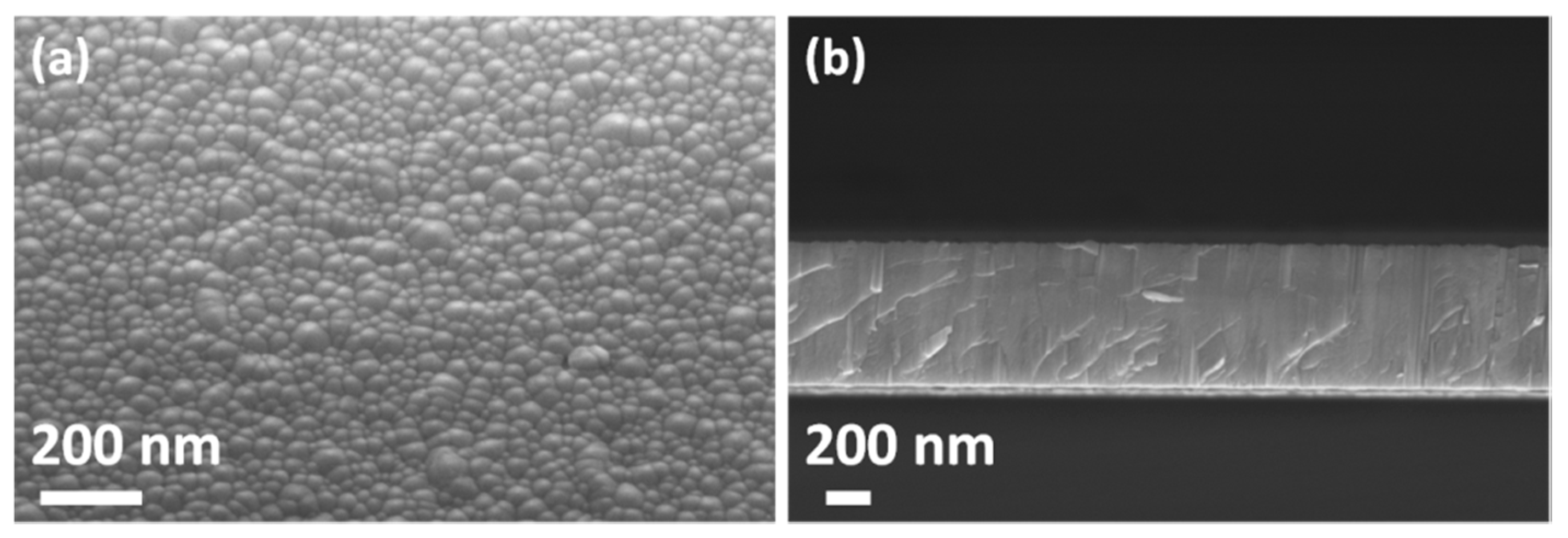
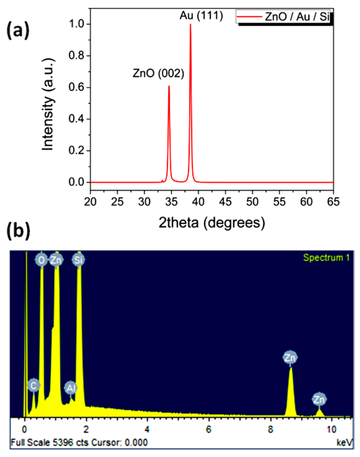
3.1. Gold Electrodes—Preparation and Characterization

The morphology and average thickness of Au metal layers were analyzed by means of FESEM analyses for the samples deposited on Polyimide foils and Si substrates, respectively. In the case of the polymeric substrate, particular attention was paid to the evaluation of the surface characteristics of the Au layer, investigating the eventual presence of cracks, voids or detachments as well. Figure 1 shows FESEM images of a 100 nm-thick Au layer deposited on Polyimide foil (Figure 1a) and Si substrate (Figure 1b). A smooth surface, characterized by nanometer-sized, closely-packed grains, was observed. Even if no adhesion promoter was used, the Au layer showed a continuous and uniform structure on the whole area without evidence of cracks. All of these factors witnessed the good mechanical adhesion of the Au film to the polymeric substrate. This is further visible in the inset of Figure 1a, which shows a picture representative of the flexible Au/Polyimide structure. The good mechanical quality of the metal layer directly deposited on the flexible Polyimide foil is further noticed after bending the flexible specimen, indeed no mechanical degradation affecting the metal was observed, confirming the good adhesion of the Au layer to the polymeric substrate, despite no adhesion layers being previously deposited on the uncoated polymer.
Figure 1. FESEM images of Au layers deposited on (a) Polyimide and (b) Si wafer. Inset of panel (a) shows a picture of the Au-coated Polyimide specimen.
Micromachines 06 01453 g001

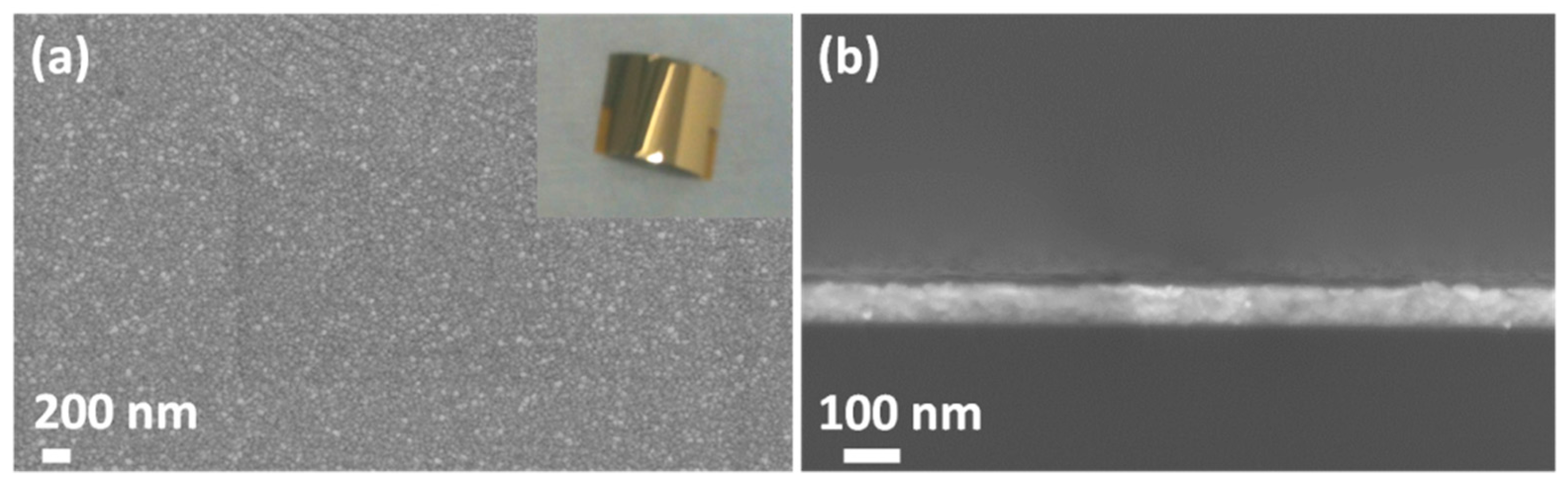
3.2. ZnO Thin Films—Preparation and Characterization

The set of deposition parameters used for growing ZnO thin films are summarized in Table 2. Figure 2 shows the surface morphology and cross-sectional nanostructure representative of a 700 nm-thick ZnO film deposited on Si/Au substrate. The surface morphology was first analyzed (Figure 2a), highlighting the presence of a fine-grained nanostructure, with an average grain size ranging between 20 and 100 nm. The cross-section of the ZnO film is shown in Figure 2b and reveals the presence of highly densely-packed, vertically-aligned nanocrystals. This aspect is representative of the columnar growth regime which took place during the thin film growth, and is typical of c-axis-(002)-oriented polycrystalline ZnO thin films [60].
Figure 2. FESEM images showing (a) the surface morphology and (b) the cross-section structure of ZnO thin films grown on Au-coated Si substrates.
Micromachines 06 01453 g002
X-Ray diffraction measurements were performed in order to analyze the crystal structure and orientation of the ZnO material. This aspect is really important. Indeed, the (002) crystallographic orientation is the one along with ZnO PE is maximized [61]. For this reason the deposition of highly c-axis-(002)-oriented films with a hexagonal wurtzite-like structure is essential for the PE response of ZnO to be promoted. The diffraction pattern collected from 700 nm-thick ZnO film grown on Si/Au substrate is shown in Figure 3a. A single diffraction peak positioned at 34.35° was detected. This can be ascribed to the family of (002)-oriented crystal planes (Joint Committee on Powder Diffraction Standards-International Centre for Diffraction Data, JCPDS-ICDD card no. 89–1397) and is representative of the presence of the hexagonal wurtzite-like crystal structure in the analyzed material. The presence of such preferential orientation also witnesses that approximately all of the crystal grains are already aligned along the desired PE (002) orientation. Therefore, no additional poling treatment is required for PE to occur.
The chemical composition of ZnO thin film was investigated by Energy-Dispersive X-ray (EDX) spectroscopy. From the EDX spectrum reported in Figure 3b it can be observed that zinc (21.93 at.%) and oxygen (41.06 at.%) are detected, as expected. However, carbon (12.15 at.%) and silicon (24.68 at.%) are visible as well, because of contaminants absorbed on the sample surface and of the Si substrate contribution, respectively. A small amount of Al (0.17 at.%) coming from the sample holder is also detected. Since, from the EDX measurement the contributions of silicon, carbon, and aluminum cannot be excluded, a precise estimation of the ZnO stoichiometry could not be carried out.
Hall effect measurements were carried out on the 700 nm-thick ZnO film in order to examine the nature of majority carriers, film resistivity, and carriers mobility and concentration as well. ZnO is a well-known n-type semiconductor. This aspect is further confirmed in the present work, since electrons were found as majority charge carriers. The measured ZnO resistivity was 4.41 · 10−3 Ω∙cm, while the carriers mobility and concentration values were 80 cm2·V−1·s−1 and 2.29 × 1017 cm−3, respectively. Generally oxygen vacancies, together with the presence of unintentional hydrogen impurities, are believed to be at the basis of the intrinsic n-type nature of ZnO-based materials [62].
The current-voltage (IV) characteristic describing the electrical behavior of 700 nm-thick ZnO thin film is shown in Figure 4. The IV response was representative of the semiconductor nature of ZnO, showing currents ranging in the order of tens of μA and a nonlinear Schottky behavior. When the applied voltage was ±40 V or more, short circuits started to be present, witnessing that breakdown phenomena occurred in the investigated ZnO sample.
Figure 3. (a) XRD pattern and (b) EDX spectrum of sputtered ZnO thin films.
Micromachines 06 01453 g003
Figure 4. IV curve measured on a 700 nm-thick ZnO thin film.
Micromachines 06 01453 g004

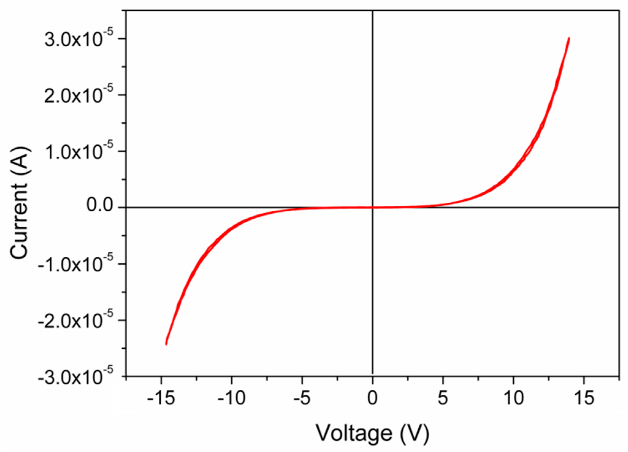
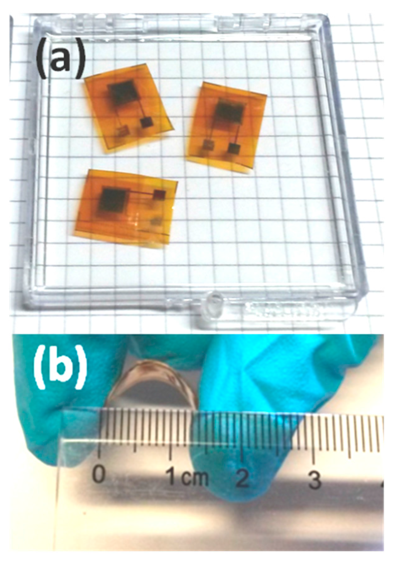
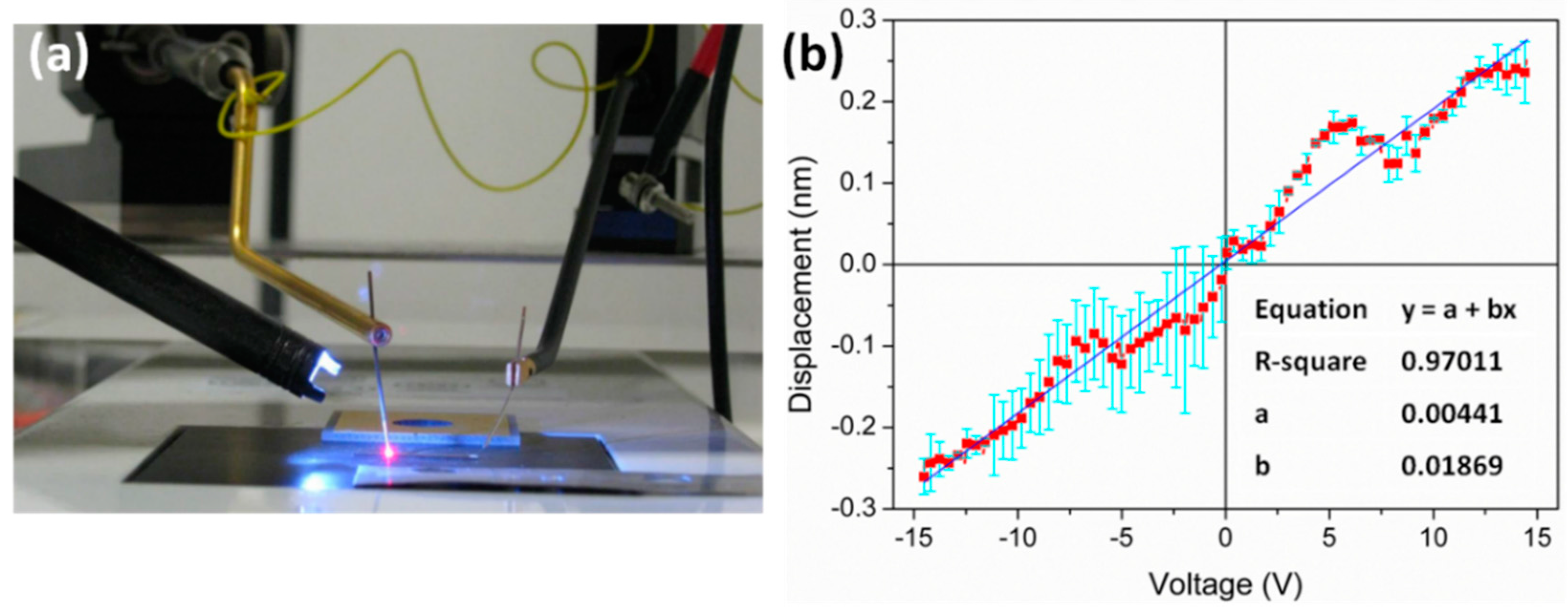
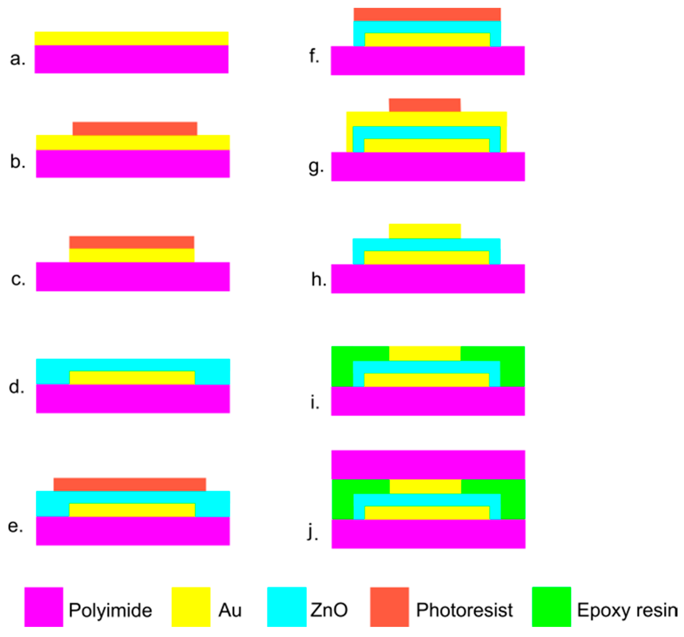
3.3. Device Fabrication and Characterization

The design of the final PPT structure in its CPE configuration is qualitatively presented in Figure 5.
Figure 5. Sketch of the main parts composing the PPT structure in the CPE configuration—Top view.
Micromachines 06 01453 g005
Each transducer was composed of:
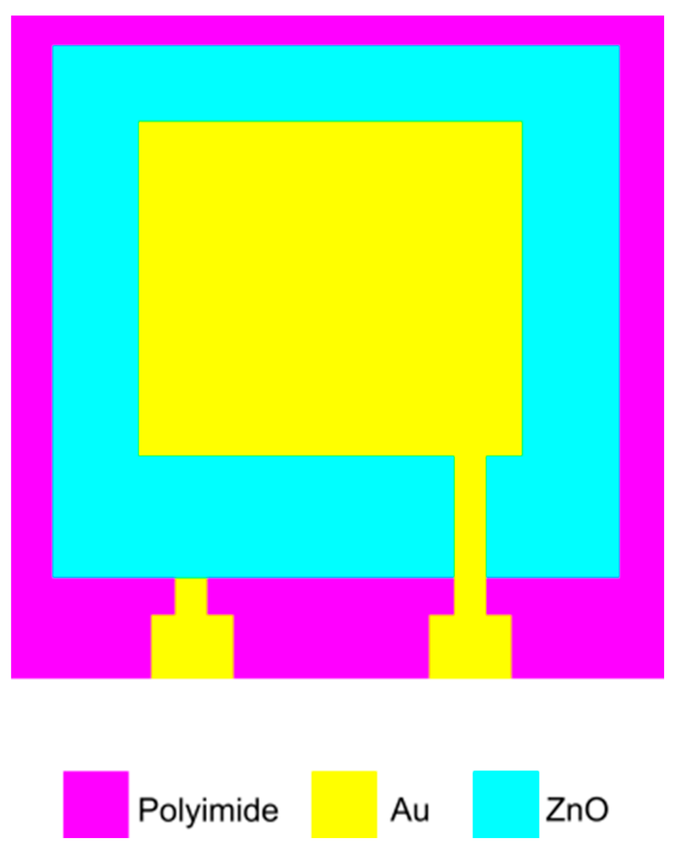
  • Lower and upper Polyimide supports (total patch dimensions: 10 mm × 10 mm);
  • 100 nm-thick Au bottom electrode (5 mm × 5 mm);
  • 700 nm-thick ZnO piezoceramic layer (8 mm × 8 mm);
  • 100 nm-thick Au top electrode (4 mm × 4 mm).
The process steps followed for the fabrication of the transducers are represented in Figure 6. The first steps (a–c) consisted in the preparation of the patterned Au bottom electrode deposited on Polyimide foils by optical lithography and wet etching processes. A 1 µm–thick positive photoresist (HPR504) was deposited onto the samples. The desired geometry was then obtained by aligning a Mylar® mask with the UV radiation, exposing to UV radiation, and developing the photoresist. The Au layer was then removed by wet etching with a solution of KI:I2:H2O (4 g:1 g:40 mL). Finally, the patterned samples were rinsed in deionized water and then with acetone and isopropanol to remove the unexposed photoresist. A 700 nm-thick ZnO film was then deposited onto the patterned Au-coated Polyimide substrates (d–f). The same patterning procedure described so far was performed to define the geometry of the ZnO layer and top electrode (g–h).
The last step of the fabrication process (Figure 6i,j) consisted in the assembly of the final structure. This was obtained by gluing the upper and lower Polyimide foils with an epoxy resin suitable for space applications. The assembly of the final transducer requires the use of adhesives in order to fix the different parts together, guaranteeing insulation between facing electrodes, electrical continuity between metallic electrodes, and the active layer and the sealing of the structure from the external environment, without worsening the flexibility of the device. The adhesive used for the assembly was, thus, selected among those commercially available, by considering thermal and electrical conductivity, mechanical, and out-gassing characteristics of the commercial products. On the basis of these considerations, an epoxy resin was purchased from ELANTAS (Epoxylite TSA 220, Wesel, Germany) and selected for being an electrically-insulating epoxide resistant to high strains, bondable to the required materials, curable from room to high temperature, stable during the service temperature range, and characterized by low outgassing values. The curing procedure consisted in a thermal treatment performed in air at 165 °C for 12 h.
Figure 6. Flow-chart describing the process steps of the PPT in CPE configuration fabrication process: (ah) deposition and patterning of the electrodes and ZnO thin film; (i,j) assembly of the final PPT structure.
Micromachines 06 01453 g006
Table 3 summarizes some technical characteristics of the prototypes prepared by following the fabrication process reported in Figure 6 and the curing process described above.
Table 3. Technical characteristics of the PPT prototypes.
ParameterValue
Active Area4 mm × 4 mm
Active layer thickness900 nm
Minimum curvature radius6 mm
Operating temperature−40 °C up to 80 °C
Breakdown voltage *±40 V
d3312.3 pm/V
Typical operating voltage±15 V
Typical operating frequency100 Hz
* Tested in the frequency range between 1 and 100 Hz.
In order to qualify the operation of the prepared prototypes as piezopolymeric transducers, the converse PE effect was evaluated on the samples, as shown in Figure 7. Measurements were performed by using the PES setup described in the Experimental Section. An electric voltage (±15 V) was applied on the PPT and the PE-induced mechanical displacement recorded by a single-point laser vibrometer (see Figure 8a). The displacement vs. voltage curve representative of the converse PE behavior of the investigated PPT structures is shown in Figure 8b together with the corresponding linear fit.
Figure 7. Image representative of the different PPT prototypes (a) as prepared and (b) under bending conditions.
Micromachines 06 01453 g007
Figure 8. (a) Picture of the PES setup used for piezoelectric characterization; (b) Mechanical displacement vs. applied voltage measured on the PPT prototypes.
Micromachines 06 01453 g008
An almost-linear behavior was obtained and no hysteresis phenomena were observed. This last aspect was expected, since ZnO does not show the presence of ferroelectric domains, being a non-perovskite PE material. Thus, the PE characteristic is expected to be quite linear, as for other non-centrosymmetric materials like AlN [63]. However, some deviations from a perfect linear behavior are visible (R-square ~0.97). These are mainly ascribed to additional contributions coming from the substrate bending, which cannot be excluded during the measurements, with our setup. The measured peak-to-peak mechanical displacement was around 530 nm. From the slope of the linear characteristic an estimation of the d33 PE coefficient was also possible, with an average value of 12.3 pm/V that well agrees with the 12.84 pm/V theoretically determined by direct first-principles density functional calculations [64]. The direct PE effect of flexible ZnO-based structures very similar to the ones reported in this work was already investigated and reported in a previously published paper [39]. In that case a PE output voltage generation of 0.361 V was obtained for a 700 nm-thick ZnO film under the application of a periodical mechanical stimulus of 30 N. The sensitiveness of our sputtered ZnO thin films towards input mechanical forces was thus already pointed out, and further supported the investigation of such materials as PE transducers for HMS.
The device described in this paper was conceived to be coupled to the cylindrical fuel tank of a system launcher. Normally those vessels are fabricated by means of filament winding using carbon fibers, an extremely tough material, in which the formation and propagation of a crack, due to accidental impacts or mechanical stresses could eventually result in mission failure and payload loss. The real-time monitoring of eventual crack formation/propagation is thought to be done by injecting a train of Lamb waves through our PPT and using the same device as a receiver to correlate eventual echoes to the cracks. The material choice and trade-off, the device design, and fabrication, were all conceived to provide an engineering solution to the onboard requirements. As an example, the breakdown voltage of 40 V well fits with the standard onboard power bus (28 V).
Both read-out and control circuitry fabrication and testing, as well as PPT operation in the relevant environment, are outside of the scope of the present paper.

4. Conclusions

This work reports about the fabrication of conformable, reusable, and reproducible piezopolymeric transducers (PPT) for health monitoring systems in space applications. Suitable materials and design for the fabrication of the PPT structures were defined, on the basis of fundamental requirements for HMS applications. The design of the PPT consisted of a piezoceramic layer coupled to a pair of flexible polymeric patches covered with metal layers acting as electrodes. Sputtering was selected as the synthesis technique for growing all the involved materials, while Au and ZnO were selected as the electrode material and the piezoceramic, respectively. In particular, ZnO was considered a promising candidate thanks to its biocompatibility and compatibility to the space environment, thus representing a valid alternative to the conventional lead-based, toxic PZT. Suitable deposition conditions were selected for the sputter deposition of high-quality Au electrodes and PE ZnO thin films on flexible Polyimide substrates. The fabrication process for the PPT structure consisted in the following steps. Au metal layers were deposited on Polyimide foils and patterned in order to get the desired bottom electrode geometry. After that, ZnO thin films were deposited onto the Au/Polyimide substrates and patterned. Finally, the Au top electrode was deposited on the ZnO/Au/Polyimide structure, and patterned again. Wet-chemical etching and optical lithography were performed for patterning the different parts of the transducer. An epoxy resin suitable for space applications was selected among those commercially available and used for the final assembly of the PPT structure, which consisted in a thermal bonding procedure needed to fix the upper Polyimide foil to the underlying Au/ZnO/Au/Polyimide structure. Following this fabrication process, different PPT prototypes were successfully prepared and their converse PE behavior evaluated by applying an electric voltage across the ZnO layer, and measuring the induced mechanical displacement. In this way an estimation of the d33 PE coefficient was also possible, with a measured value of 12.3 pm/V, in agreement with the one theoretically predicted for ZnO. Our results encourage the use of PE ZnO thin films for the fabrication of flexible and conformable PE transducers for HMS applications.

Acknowledgments

Research was funded by Regione Piemonte, Piattaforma Aerospazio, under the STEPS2 project (Sistemi e TEcnologie Per lo Spazio 2).

Author Contributions

This work was conceived and scientifically coordinated by Alessandro Chiolerio. Marco Laurenti performed ZnO depositions and their characterization. Denis Perrone and Alessio Verna designed and carried out all the technological processes for patterning the different parts composing the transducers. The final assembly of the transducers and their piezoelectric characterization was carried out by Marco Laurenti. This paper was written by Marco Laurenti with the contribution of Alessandro Chiolerio. This work was carried out under the further supervision of Candido F. Pirri.

Conflicts of Interest

The authors declare no conflict of interest.

References

  1. Dodds, J.S.; Meyers, F.N.; Loh, K.J. Piezoelectric nanocomposite sensors assembled using zinc oxide nanoparticles and poly(vinylidene fluoride). Smart Struct. Syst. 2013, 12, 055–071. [Google Scholar] [CrossRef]
  2. Yoon, H.S.; Jung, D.; Kim, J.H. Lamb wave generation and detection using piezoceramic stack transducers for structural health monitoring applications. Smart Mater. Struct. 2012, 21, 055019. [Google Scholar] [CrossRef]
  3. Joshi, S.; Hegde, G.M.; Nayak, M.M.; Rajanna, K. A novel piezoelectric thin film impact sensor: Application in non-destructive material discrimination. Sens. Actuators A 2013, 199, 272–282. [Google Scholar] [CrossRef]
  4. Yan, S.; Wu, J.; Sun, W.; Ma, H.; Yan, H. Development and application of structural health monitoring system based on piezoelectric sensors. Int. J. Distrib. Sens. Netw. 2013, 270927, 12. [Google Scholar] [CrossRef]
  5. Ko, J.M.; Ni, Y.Q. Technology developments in structural health monitoring of large-scale bridges. Eng. Struct. 2005, 27, 1715–1725. [Google Scholar] [CrossRef]
  6. Lu, Y.; Wang, X.; Tang, J.; Ding, Y. Damage detection using piezoelectric transducers and the Lamb wave approach: II. Robust and quantitative decision making. Smart Mater. Struct. 2008, 17, 025034. [Google Scholar] [CrossRef]
  7. Betz, D.C.; Thursby, G.; Culshaw, B.; Staszewski, W.J. Structural damage location with fiber bragg grating rosettes and lamb waves. Struct. Health Monit. 2007, 6, 299–308. [Google Scholar] [CrossRef]
  8. Barazanchy, D.; Martinez, M.; Rocha, B.; Yanishevsky, M. A hybrid structural health monitoring system for the detection and localization of damage in composite structures. J. Sens. 2014, 109403. [Google Scholar] [CrossRef]
  9. Chiolerio, A.; Roppolo, I.; Sangermano, M. Radical diffusion engineering: Tailored nanocomposite materials for piezoresistive inkjet printed strain measurement. RSC Adv. 2013, 3, 3446–3452. [Google Scholar] [CrossRef]
  10. Giorgio, I.; Galantucci, L.; Della Corte, A.; del Vescovo, D. Piezo-electromechanical smart materials with distributed arrays of piezoelectric transducers: Current and upcoming applications. Int. J. Appl. Electromagn. Mech. 2015, 47, 1051–1084. [Google Scholar] [CrossRef]
  11. Dell’Isola, F.; Vestroni, F.; Vidoli, S. Structural-damage detection by distributed piezoelectric transducers and tuned electric circuits. Res. Nondestruct. Eval. 2005, 16, 101–118. [Google Scholar] [CrossRef]
  12. Dell’Isola, F.; Vestroni, F.; Vidoli, S. A class of electro-mechanical systems: Linear and nonlinear dynamics. J. Theor. Appl. Mech. 2002, 40, 47–71. [Google Scholar]
  13. Su, Z.; Ye, L.; Ye, L. Guided lamb waves for identification of damage in composite structures: A review. J. Sound Vib. 2006, 295, 753–780. [Google Scholar] [CrossRef]
  14. Giurgiutiu, V.; Zagrai, A. Damage detection in thin plates and aerospace structures with the electro-mechanical impedance method. Struct. Health Monit. 2005, 4, 99–118. [Google Scholar] [CrossRef]
  15. Ciang, C.C.; Lee, J.R.; Bang, H.J. Structural health monitoring for a wind turbine system: A review of damage detection methods. Meas. Sci. Technol. 2008, 19, 122001. [Google Scholar] [CrossRef]
  16. Daré de Almeida, V.A.; Guimarães Baptista, F.; de Aguiar, P.R. Piezoelectric transducers assessed by the pencil lead break for impedance-based structural health monitoring. IEEE Sens. J. 2015, 15, 693–702. (In Portuguese) [Google Scholar] [CrossRef]
  17. Gary, J.; Hamstad, M.A. On the far-field structure of waves generated by a pencil lead break on a thin plate. J. Acoust. Emiss. 1994, 12, 157–170. [Google Scholar]
  18. Sohn, H.; Park, G.; Wait, J.R.; Limback, N.P.; Farrar, C.R. Wavelet-based active sensing for delamination detection in composite structure. Smart Mater. Struct. 2004, 13, 153–160. [Google Scholar] [CrossRef]
  19. Wang, C.S.; Wu, F.; Chang, F.K. Structural health monitoring from fiber-reinforced composites to steel-reinforced concrete. Smart Mater. Struct. 2001, 10, 548. [Google Scholar] [CrossRef]
  20. Park, S.; Yun, C.B.; Roh, Y.; Lee, J.J. PZT-based active damage detection techniques for steel bridge components. Smart Mater. Struct. 2006, 15, 957. [Google Scholar] [CrossRef]
  21. Law, C.W.; Tong, K.Y.; Li, J.H.; Li, K. Effect of pyrolysis temperature on the characteristics of PZT films deposited by the sol-gel method. Thin Solid Films 1998, 335, 220–224. [Google Scholar] [CrossRef]
  22. Chiolerio, A.; Quaglio, M.; Lamberti, A.; Celegato, F.; Balma, D.; Allia, P. Magnetoelastic coupling in multilayered ferroelectric/ferromagnetic thin films: A quantitative evaluation. Appl. Surface Sci. 2012, 258, 8072–8077. [Google Scholar] [CrossRef]
  23. Makino, H.; Kamiya, N. Effects of DC electric fields on mechanical properties of piezoelectric ceramics. Jpn. J. Appl. Phys. 1994, 33, 5323–5327. [Google Scholar] [CrossRef]
  24. Watanabe, S.; Fujiu, T.; Fujii, T. Effect of poling on piezoelectric properties of lead zirconate titanate thin films formed by sputtering. Appl. Phys. Lett. 1995, 66, 1481–1483. [Google Scholar] [CrossRef]
  25. Lin, B.; Giurgiutiu, V. Modeling and testing of PZT and PVDF piezoelectric wafer active sensors. Smart Mater. Struct. 2006, 15, 1085–1093. [Google Scholar] [CrossRef]
  26. Monkhouse, R.; Wilcox, P.; Cawley, P. Flexible interdigital PVDF transducers for the generation of Lamb waves in structures. Ultrasonics 1997, 35, 489–498. [Google Scholar] [CrossRef]
  27. Furukawa, T.; Ishida, K.; Fukada, E. Piezoelectric properties in the composite systems of polymers and PZT ceramics. J. Appl. Phys. 1979, 50, 4904–4912. [Google Scholar] [CrossRef]
  28. Venkatragavaraj, E.; Satish, B.; Vinod, P.R.; Vijaya, M.S. Piezoelectric properties of ferroelectric PZT-polymer composites. J. Phys. D: Applied Physics 2001, 34, 487. [Google Scholar] [CrossRef]
  29. Dietze, M.; Es-Souni, M. Structural and functional properties of screen-printed PZT–PVDF-TrFE composites. Sens. Actuators A Phys. 2008, 143, 329–334. [Google Scholar] [CrossRef]
  30. Panda, P.K. Review: Environmental friendly lead-free piezoelectric materials. J. Mater. Sci. 2009, 44, 5049–5062. [Google Scholar] [CrossRef]
  31. Park, K.I.; Xu, S.; Liu, Y.; Hwang, G.T.; Kang, S.J.L.; Wang, Z.L.; Lee, K.J. Piezoelectric BaTiO3 thin film nanogenerator on plastic substrates. Nano Lett. 2010, 10, 4939–4943. [Google Scholar] [CrossRef] [PubMed]
  32. Chiolerio, A.; Lombardi, M.; Guerriero, A.; Canavese, G.; Stassi, S.; Gazia, R.; Cauda, V.; Manfredi, D.; Chiodoni, A.; Verna, A.; et al. Effect of the fabrication method on the functional properties of BaTiO3: PVDF nanocomposites. J. Mater. Sci. 2013, 48, 6943–6951. [Google Scholar] [CrossRef]
  33. Iriarte, G.F.; Rodriguez, J.G.; Calle, F. Synthesis of c-axis oriented AlN thin films on different substrates: A review. Mater. Res. Bull. 2010, 45, 1039–1045. [Google Scholar] [CrossRef]
  34. Youssef, S.; Combette, P.; Podlecki, J.; Asmar, R.A.; Foucaran, A. Structural and optical characterization of ZnO thin films deposited by reactive RF magnetron sputtering. Cryst. Growth Des. 2009, 9, 1088–1094. [Google Scholar] [CrossRef]
  35. Gualtieri, J.G.; Kosinski, J.; Ballato, A. Piezoelectric materials for acoustic wave applications. IEEE Trans. Ultrason. Ferroelectr. Freq. Control 1994, 41, 53–59. [Google Scholar] [CrossRef]
  36. Jackson, N.; Keeney, L.; Mathewson, A. Flexible-CMOS and biocompatible piezoelectric AlN material for MEMS applications. Smart Mater. Struct. 2013, 22, 115033. [Google Scholar] [CrossRef]
  37. Ottone, C.; Laurenti, M.; Motto, P.; Stassi, S.; Demarchi, D.; Cauda, V.A. ZnO nanowires: Synthesis approaches and electrical properties. In Nanowires. Synthesis, Electrical Properties and Uses in Biological Systems; Nova Publisher: New York, NY, USA, 2014; pp. 1–57. [Google Scholar]
  38. Gazia, R.; Motto, P.; Stassi, S.; Sacco, A.; Virga, A.; Lamberti, A.; Canavese, G. Photodetection and piezoelectric response from hard and flexible sponge-like ZnO-based structures. Nano Energy 2013, 2, 1294–1302. [Google Scholar] [CrossRef]
  39. Laurenti, M.; Stassi, S.; Lorenzoni, M.; Fontana, M.; Canavese, G.; Cauda, V.; Pirri, C.F. Evaluation of the piezoelectric properties and voltage generation of flexible zinc oxide thin films. Nanotechnology 2015, 26, 215704. [Google Scholar] [CrossRef] [PubMed]
  40. Chiolerio, A.; Roppolo, I.; Cauda, V.; Crepaldi, M.; Bocchini, S.; Bejtka, K.; Verna, A.; Pirri, C.F. Ultraviolet mem-sensors: Flexible anisotropic composites featuring giant photocurrent enhancement. Nano Res. 2015, 8, 1956–1963. [Google Scholar] [CrossRef]
  41. Laurenti, M.; Verna, A.; Fontana, M.; Quaglio, M.; Porro, S. Selective growth of ZnO nanowires on substrates patterned by photolithography and inkjet printing. Appl. Phys. A Mater. Sci. Proces. 2014, 117, 901–907. [Google Scholar] [CrossRef]
  42. Yi, G.C.; Wang, C.; Park, W.I. ZnO nanorods: Synthesis, characterization and applications. Semicond. Sci. Technol. 2005, 20, S22–S34. [Google Scholar] [CrossRef]
  43. Xi, Y.; Hu, C.G.; Han, X.Y.; Xiong, Y.F.; Gao, P.X.; Liu, G.B. Hydrothermal synthesis of ZnO nanobelts and gas sensitivity property. Solid State Commun. 2007, 141, 506–509. [Google Scholar] [CrossRef]
  44. Gao, W.; Li, Z. ZnO thin films produced by magnetron sputtering. Ceram. Int. 2004, 30, 1155–1159. [Google Scholar] [CrossRef]
  45. Tsoutsouva, M.G.; Panagopoulos, C.N.; Papadimitriou, D.; Fasaki, I.; Kompitsas, M. ZnO thin films prepared by pulsed laser deposition. Mater. Sci. Eng. B 2011, 176, 480–483. [Google Scholar] [CrossRef]
  46. Znaidi, L. Sol–gel-deposited ZnO thin films: A review. Mater. Sci. Eng. B 2010, 174, 18–30. [Google Scholar] [CrossRef]
  47. Shishodia, P.K.; Kim, H.J.; Wakahara, A.; Yoshida, A.; Shishodia, G.; Mehra, R.M. Plasma enhanced chemical vapor deposition of ZnO thin films. J. Non-Cryst. Solids 2006, 352, 2343–2346. [Google Scholar] [CrossRef]
  48. Malm, J.; Sahramo, E.; Perälä, J.; Sajavaara, T.; Karppinen, M. Low-temperature atomic layer deposition of ZnO thin films: Control of crystallinity and orientation. Thin Solid Films 2011, 519, 5319–5322. [Google Scholar] [CrossRef]
  49. Laurenti, M.; Canavese, G.; Sacco, A.; Fontana, M.; Bejtka, K.; Castellino, M.; Pirri, C.F.; Cauda, V. Nanobranched ZnO structure: p-type doping induces piezoelectric voltage generation and ferroelectric-photovoltaic effect. Adv. Mater. 2015, 27, 4218–4223. [Google Scholar] [CrossRef] [PubMed]
  50. Laurenti, M.; Garino, N.; Porro, S.; Fontana, M.; Gerbaldi, C. Zinc oxide nanostructures by chemical vapour deposition as anodes for Li-ion batteries. J. Alloys Compd. 2015, 640, 321–326. [Google Scholar] [CrossRef]
  51. Lamberti, A.; Sacco, A.; Laurenti, M.; Fontana, M.; Pirri, C.F.; Bianco, S. Sponge-like ZnO nanostructures by low temperature water vapor-oxidation method as dye-sensitized solar cell photoanodes. J. Alloys Compd. 2014, 615, S487–S490. [Google Scholar] [CrossRef]
  52. Laurenti, M.; Cauda, V.; Gazia, R.; Fontana, M.; Rivera, V.F.; Bianco, S.; Canavese, G. Wettability control on ZnO nanowires driven by seed layer properties. Eur. J. Inorg. Chem. 2013, 2013, 2520–2527. [Google Scholar] [CrossRef]
  53. Dodds, J.S.; Meyers, F.N.; Loh, K.J. Piezoelectric characterization of PVDF-TrFE thin films enhanced with ZnO nanoparticles. IEEE Sens. J. 2012, 12, 1889–1890. [Google Scholar] [CrossRef]
  54. Dodds, J.S.; Meyers, F.N.; Loh, K.J. Enhancing the piezoelectric performance of PVDF-TrFE thin films using zinc oxide nanoparticles. In Proceedings of the Sensors and Smart Structures Technologies for Civil, Mechanical, and Aerospace Systems, San Diego, CA, USA, 11 March 2012.
  55. Gullapalli, H.; Vemuru, V.S.; Kumar, A.; Botello-Mendez, A.; Vajtai, R.; Nagarajaiah, S.; Terrones, M.; Ajayan, P.M. Flexible piezoelectric ZnO-paper nanocomposite strain sensor. Small 2010, 6, 1641–1646. [Google Scholar] [CrossRef] [PubMed]
  56. Loh, K.; Chang, D. Zinc oxide nanoparticle-polymeric thin films for dynamic strain sensing. J. Mater. Sci. 2010, 46, 228–237. [Google Scholar] [CrossRef]
  57. Laurenti, M.; Verna, A.; Chiolerio, A. Evidence of negative capacitance in piezoelectric ZnO thin films sputtered on interdigital electrodes. ACS Appl. Mater. Interfaces 2015, in press. [Google Scholar] [CrossRef] [PubMed]
  58. Prepelita, P.; Craciun, V.; Filipescu, M.; Garoi, F. Sputtered zinc oxide thin films deposited on polyimide substrate and annealing effect on the physical properties. Thin Solid Films 2013, 545, 564–570. [Google Scholar] [CrossRef]
  59. Changji, H.; Zhenhui, H.; Weichun, F.; Qi, Z. Influence of deposition pressure on the adhesion of ZnO thin films deposited by cathodic vacuum arc deposition on polyimide foil substrates. J. Phys. D Appl. Phys. 2009, 42, 185303. [Google Scholar] [CrossRef]
  60. Mirica, E.; Kowach, G.; Evans, P.; Du, H. Morphological evolution of ZnO thin films deposited by reactive sputtering. Cryst. Growth Des. 2004, 4, 147–156. [Google Scholar] [CrossRef]
  61. Gardeniers, J.G.E.; Rittersma, Z.M.; Burger, G.J. Preferred orientation and piezoelectricity in sputtered ZnO films. J. Appl. Phys. 1998, 83, 7844–7854. [Google Scholar] [CrossRef]
  62. Bang, S.; Lee, S.; Park, J.; Park, S.; Jeong, W.; Jeon, H. Investigation of the effects of interface carrier concentration on ZnO thin film transistors fabricated by atomic layer deposition. J. Phys. D Appl. Phys. 2009, 42, 235102. [Google Scholar] [CrossRef]
  63. Trolier-McKinstry, S.; Muralt, P. Thin film piezoelectrics for MEMS. J. Electroceramics 2004, 12, 7–17. [Google Scholar] [CrossRef]
  64. Karanth, D.; Fu, H. Large electromechanical response in ZnO and its microscopic origin. Phys. Rev. B 2005, 72, 064116. [Google Scholar] [CrossRef]

