
Effects of Laser Operating Parameters on Piezoelectric Substrates Micromachining with Picosecond Laser


Abstract
:1. Introduction
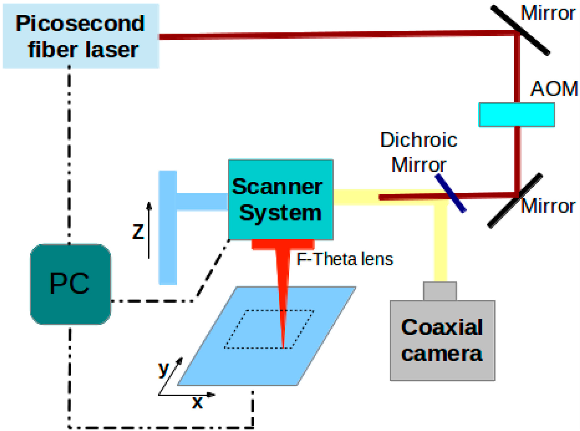
2. Experimental Section


| Parameter (units) | Values |
|---|---|
| Scan speed (mm·s−1) | 5, 10, 20, 30, 40, 50 |
| Scan number | 1, 2, 3, 4, 5, 6, 7, 8, 9, 10 |
| Fluence (J·cm−2) | 0.62, 0.93, 1.24, 1.55, 1.86, 2.17, 2.48, 2.79, 3.1 |
| Repetition rate (kHz) | 33 |

| Properties (units) | AT-cut quartz | LiNbO3 | LiTaO3 |
|---|---|---|---|
| Density (kg/m3) | 2684 | 4640 | 7450 |
| Heat Capacity (J/K/mol) | 741 | 89 | 100 |
| Thermal conductivity (W/m/K) | 3.2 | 5.6 | 4.6 |
| Melting point (°C) | 1740 | 1350 | 1605 |
| Transmittance Range (nm) | 400–3500 | 350–5000 | 400–5000 |
3. Results and Discussion
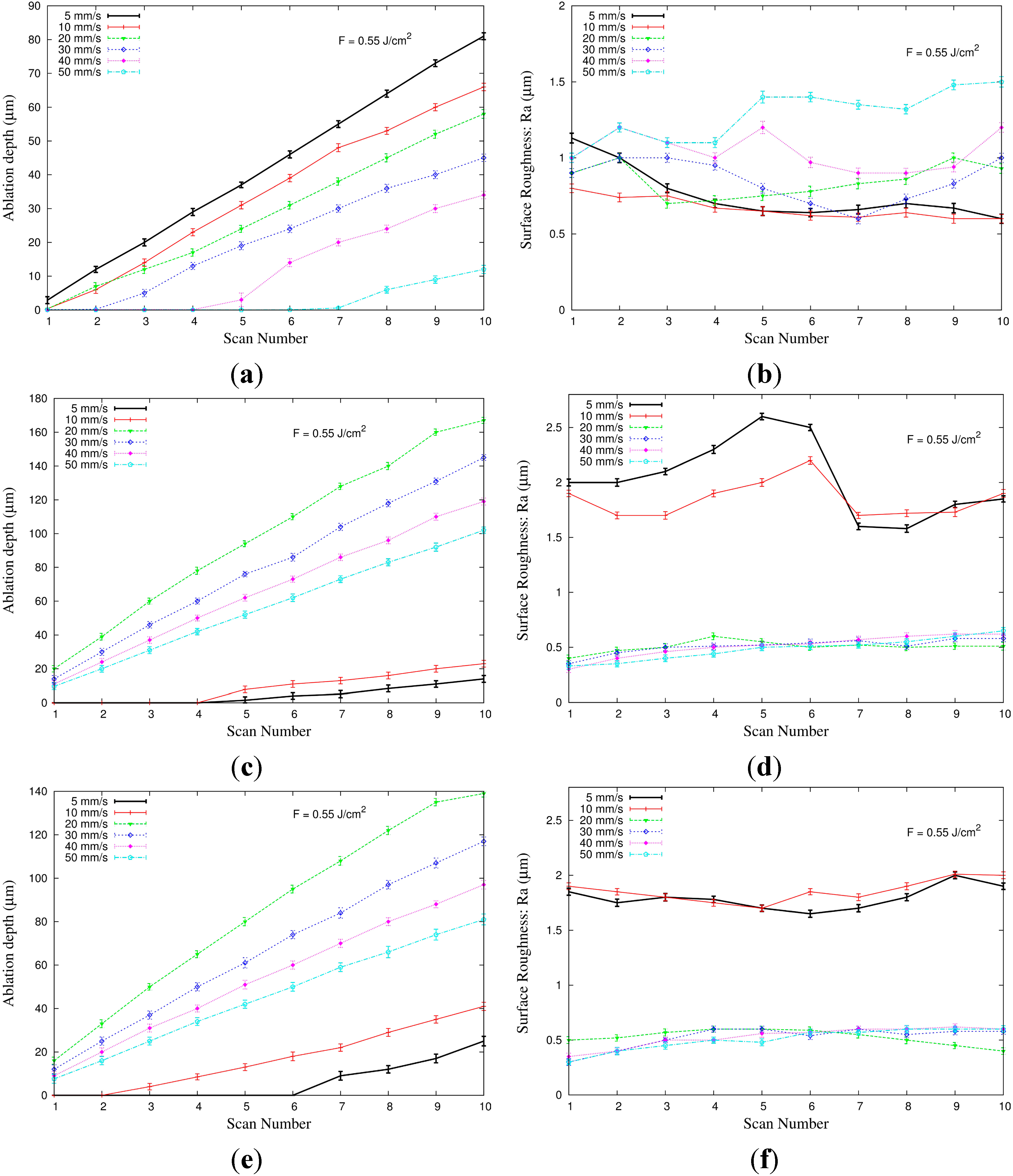
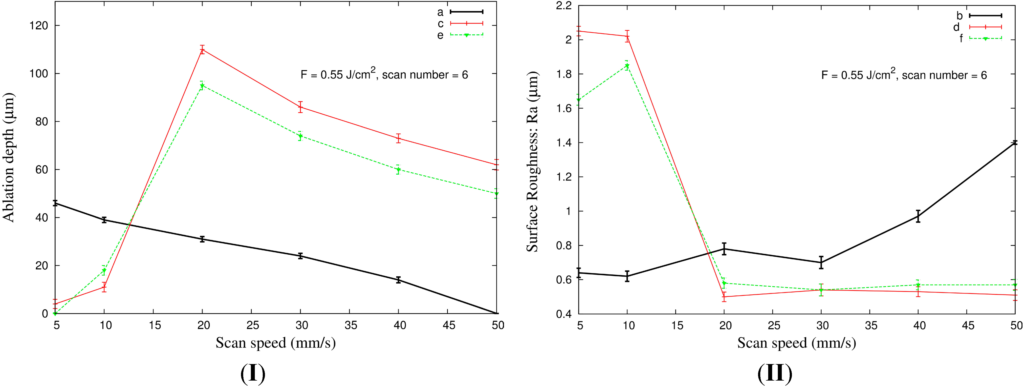
3.1. Effects of Scan Number and Scan Speed

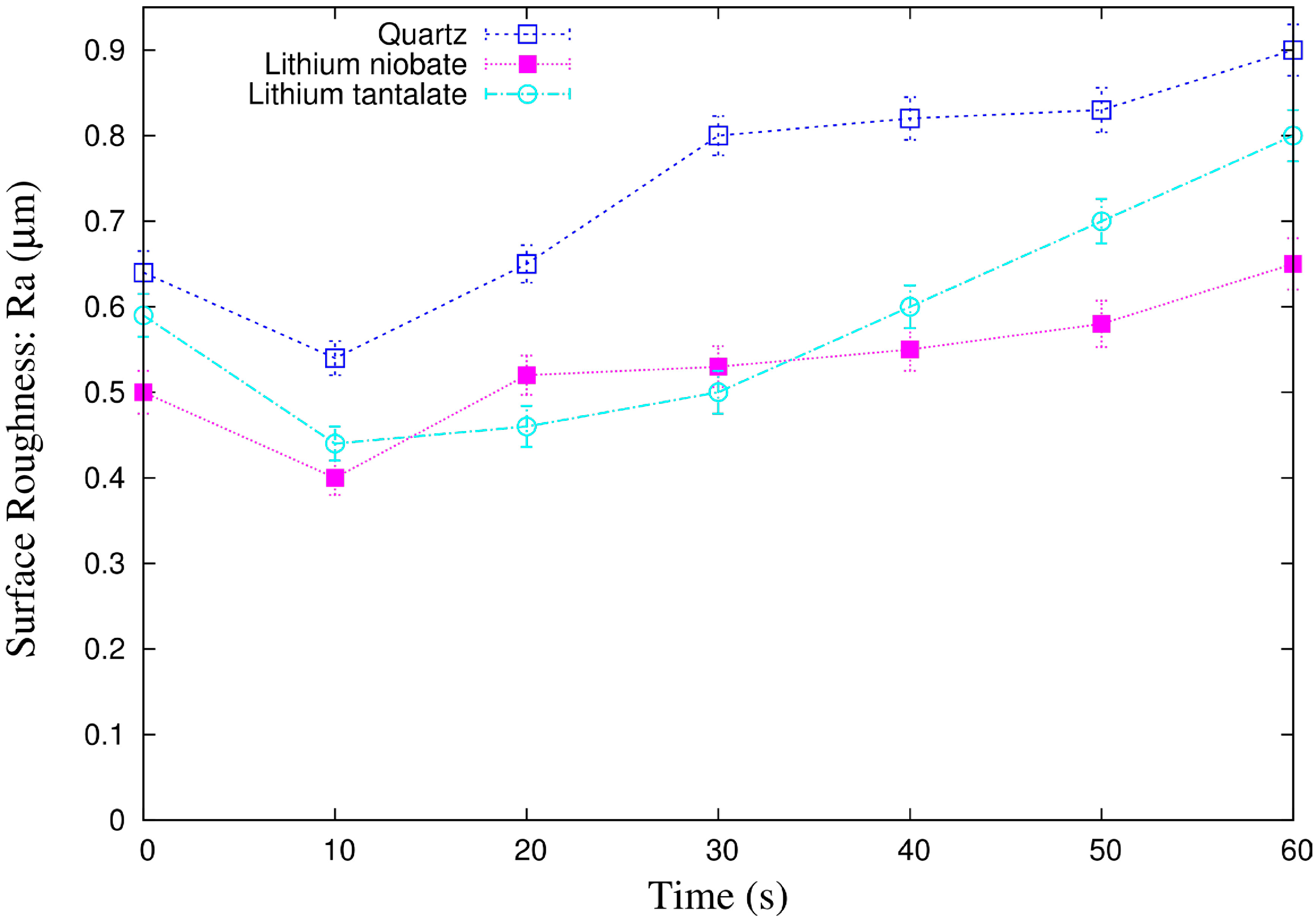
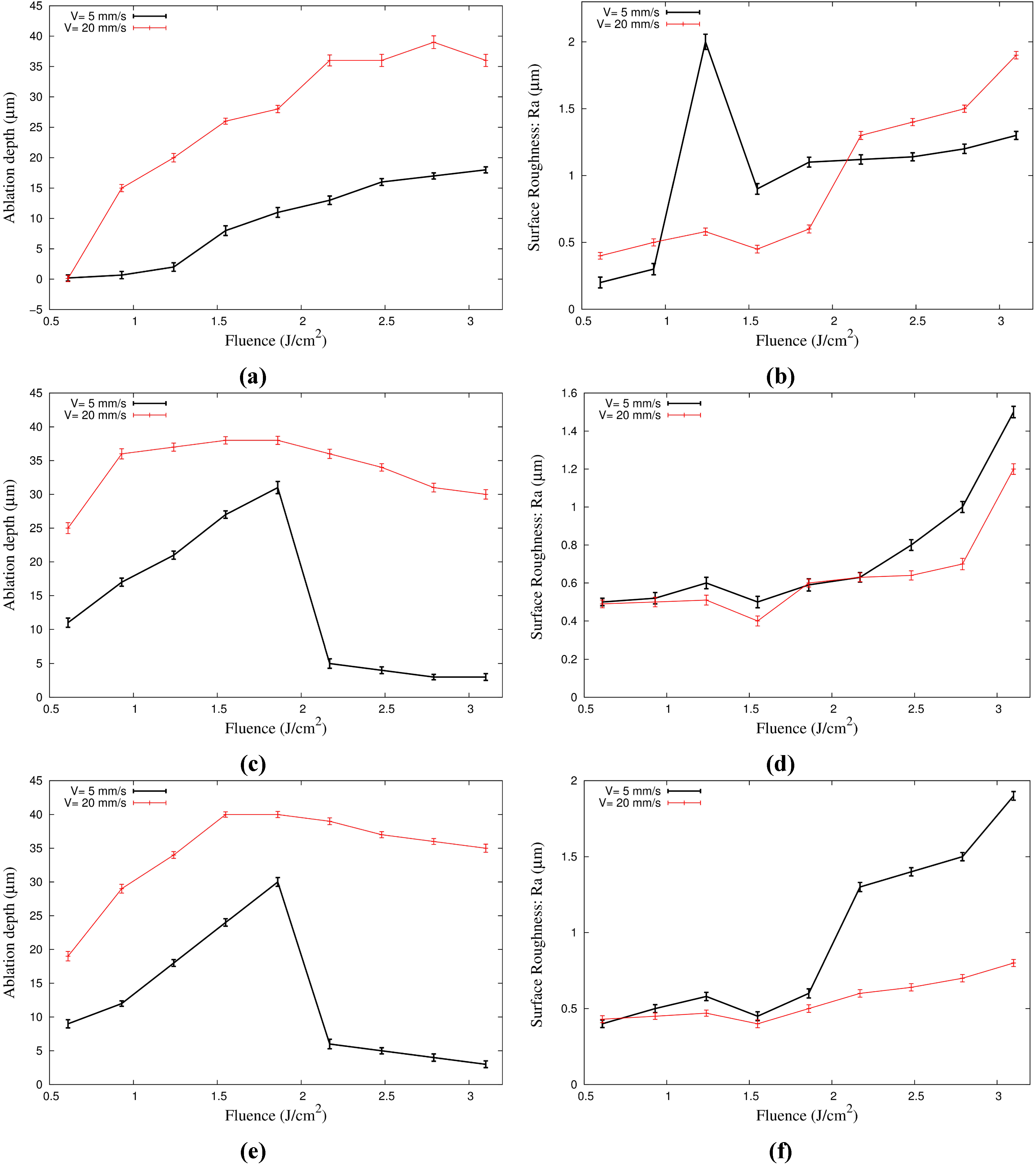
3.2. Effect of Fluence

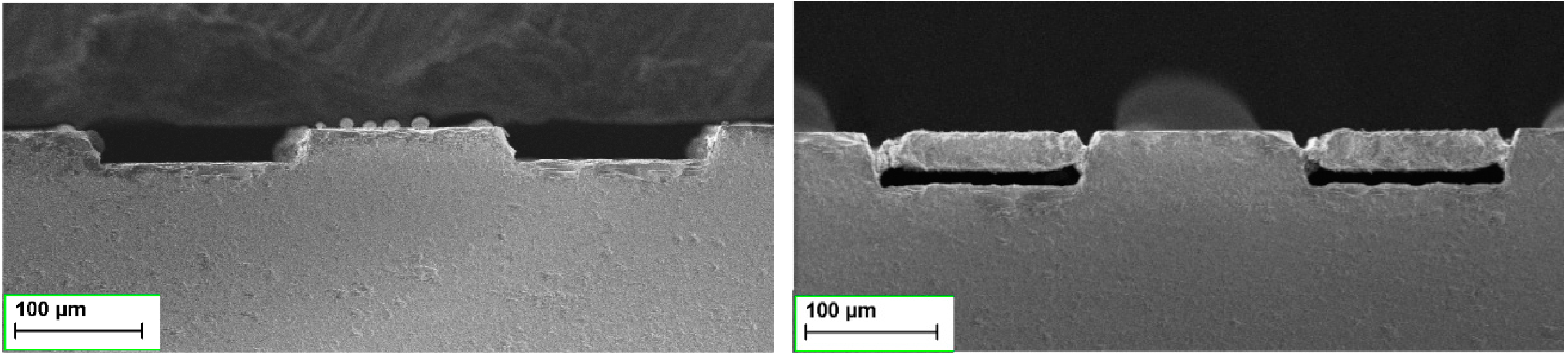
3.3. Ablation Trench Shapes
| Shape | Scan speeds | 0.61 J·cm−2 | 1.55 J·cm−2 | 3.1 J·cm−2 |
|---|---|---|---|---|
| AT-cut quartz | 5 mm·s−1 |  | 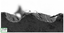 | 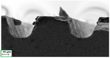 |
| 20 mm·s−1 | 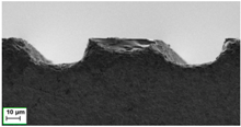 | 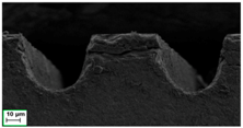 | 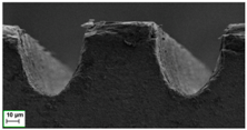 | |
| LiNbO3 | 5 mm·s−1 |  |  | 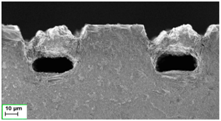 |
| 20 mm·s−1 | 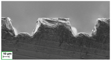 |  | 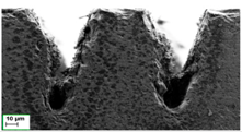 | |
| LiTaO3 | 5 mm·s−1 | 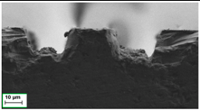 | 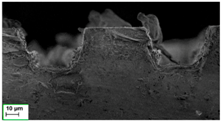 | 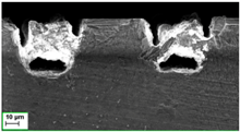 |
| 20 mm·s−1 | 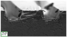 | 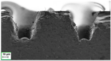 |  |
4. Conclusions
Acknowledgments
Author Contributions
Conflicts of Interest
References
- Christensena, F.K.; Mullenborn, M. Sub-band-gap laser micromachining of lithium niobate. Appl. Phys. Lett. 1995, 66, 2772–2773. [Google Scholar] [CrossRef]
- Ashby, C.I.H.; Brannon, P.J. Laser-driven chemical reaction for etching LiNbO3. Appl. Phys. Lett. 1986, 49, 475–477. [Google Scholar] [CrossRef]
- Eyett, M.; Bauerle, D. Influence of the beam spot size on ablation rates in pulsed-laser processing. Appl. Phys. Lett. 1987, 51, 2054–2055. [Google Scholar] [CrossRef]
- Ready, J.F.; Farson, D. LIA Handbook of Laser Material Processing; Laser Institute of America: Orlando, FL, USA, 2001. [Google Scholar]
- Gower, M.C.; Crafer, R.C.; Oakley, P.J. Laser Processing in Manufacturing; Chapman and Hall: London, UK, 1993. [Google Scholar]
- Gattass, R.; Mazur, E. Femtosecond laser micromachining in transparent materials. Nat. Photonics 2008, 2, 219–225. [Google Scholar] [CrossRef]
- Lim, D.; Kamotani, Y.; Cho, B.; Mazumder, J.; Takayama, S. Fabrication of microfluidic mixer and artificial vasculatures using a high-brightness diode-pumped Nd:YAG laser direct write method. Lab Chip 2003, 3, 318–323. [Google Scholar] [CrossRef] [PubMed]
- Dauer, S.; Ehlert, A.; Büttgenbach, S. Rapid prototyping of micromechanical devices using a Q-switched Nd:YAG laser with optional frequency doubling. Sens. Actuators A Phys. 1999, 76, 381–385. [Google Scholar] [CrossRef]
- Rizvi, N.H. Femtosecond laser micromachining: Current status and applications. RIKEN Rev. 2003, 50, 107–112. [Google Scholar]
- Hwang, D.J.; Choi, T.Y.; Grigoropoulos, C.P. Liquid-assisted femtosecond laser drilling of straight and three-dimentional microchannels in glass. Appl. Phys. A 2004, 79, 605–612. [Google Scholar] [CrossRef]
- Sugioka, K.; Masuda, M.; Hongo, T.; Cheng, Y.; Shihoyama, K.; Midorikawa, K. Three-dimensional microfluidic structure embedded in photostructurable glass by femtosecond laser for lab-on-chip applications. Appl. Phys. A 2004, 79, 815–817. [Google Scholar] [CrossRef]
- Giridhar, M.S.; Seong, K.; Schülzgen, A.; Khulbe, P.; Peyghambarian, N.; Mansuripur, M. Femtosecond pulsed laser micromachining of glass substrates with application to microfluidic devices. Appl. Opt. 2004, 43, 4584–4589. [Google Scholar] [CrossRef] [PubMed]
- Ho, H.; Aitchison, J.S.; Eaton, S.; Herman, P.R.; Li, J. F2-laser microfabrication forintegration optical circuits with microfluidic biochips. Proc. SPIE 2004, 5591, 96–103. [Google Scholar]
- Klank, H.; Kutter, J.P.; Geschke, O. CO2-laser micromachining and back-end processing for rapid production of PMMA-based microfluidic systems. Lab Chip 2002, 2, 242–246. [Google Scholar] [CrossRef] [PubMed]
- Ozkan, A.M.; Malshe, A.P.; Railkar, T.A.; Brown, W.D. Femtosecond laser induced periodic structure writing on diamond crystals and microclusters. Appl. Phys. Lett. 1999, 75, 3716–3718. [Google Scholar] [CrossRef]
- Will, M.; Nolte, S.; Tunnerman, A. Single and multimode waveguides in glasses manufactured with femtosecond laser pulses. Proc. SPIE 2002, 4633, 99–106. [Google Scholar]
- Zhang, Y.; Lowe, R.M.; Harvey, E.; Hannaford, P.; Endo, A. High aspect-ratio micromachining of polymers with an ultrafast laser. Appl. Surf. Sci. 2002, 186, 345–351. [Google Scholar] [CrossRef]
- Pronko, P.P.; Dutta, S.K.; Squier, J.; Rudd, J.V.; Du, D.; Mourou, G. Machining of sub-micron holes using a femtosecond laser at 800 nm. Opt. Commun. 1995, 114, 106–110. [Google Scholar] [CrossRef]
- Kim, T.; Kim, H.S.; Hetterich, M.; Jones, D.; Girkin, J.M.; Bente, E.; Dawson, M.D. Femtosecond laser machining of gallium nitride. Mater. Sci. Eng. B 2001, 82, 262–264. [Google Scholar] [CrossRef]
- Zheng, H.Y.; Zareena, A.R.; Huang, H.; Lim, G.C. Studies of femtosecond laser-processed nitinol. Mater. Sci. Forum 2003, 437, 227–280. [Google Scholar]
- Wellershoff, S.S.; Hohlfeld, J.; Gudde, J.; Matthias, E. The role of electron-phononc coupling in femtosecond laser damage of metals. Appl. Phys. A 1999, 69, S99–S107. [Google Scholar]
- Groeneveld, R.H.M.; Sprik, R.; Lagendijk, A. Femtosecond spectroscopy of electron-electron and electron-phonon energy relaxation in Ag an Au. Phys. Rev. B. 1995, 17, 11433–11445. [Google Scholar] [CrossRef]
- Chichkov, B.N.; Momma, C.; Nolte, S.; von Alvensleben, F.; Tünnermann, A. Femtosecond, picosecond and nanosecond laser ablation of solids. Appl. Phys. A 1996, 63, 109–115. [Google Scholar] [CrossRef]
- Nolte, S.; Momma, C.; Jacobs, H.; Tünnermann, A.; Chichkov, B.N.; Wellegehausen, B.; Welling, H. Ablation of metals by ultra-short laser pulses. J. Opt. Soc. Am. B 1997, 14, 2716–2722. [Google Scholar] [CrossRef]
- Breitling, D.; Ruf, A.; Dausinger, F. Fundamental aspects in machining of metals with short and ultrashort laser pulses. Proc. SPIE 2004, 5339, 49–63. [Google Scholar]
- Drogoff, L.; Vidal, F.; Laville, S.; Chaker, M.; Johnston, T.; Barthelemy, O.; Margot, J.; Sabasi, M. Laser ablated volume and depth as a function of pulse duration in aluminum targets. Appl. Opt. 2005, 44, 278–281. [Google Scholar] [CrossRef] [PubMed]
- Quartz General Material Specification. Available online: http://www.roditi.com/SingleCrystal/Quartz/QuartzHead.htm (accessed on 13 March 2014).
- MTI Webpage. SAW Grade LiNbO3 Wafers. Available online: http://www.mtixtl.com/sawgradelinbo3wafers.aspx (accessed on 13 April 2014).
- Samad, R.; Courrol, L.; Baldochi, S.; Vieira, N. Ultrashort Laser Pulses Applications. In Coherence and Ultrashort Pulse Laser Emissio; InTech: New York, NY, USA, 2012. [Google Scholar]
- Rosenfeld, A.; Lorenz, M.; Ashkenasi, D.; Stoian, R. Ultrashort-laser pulse damage threshold of transparent materials and the role of incubation. Appl. Phys. A 1999, 69, S373–S376. [Google Scholar] [CrossRef]
- Duley, W.W. UV Lasers: Effects and Applications in Materials Science; Cambridge University Press: New York, NY, USA, 1996. [Google Scholar]
- Patzel, R. An introduction to excimer lasers. In Photonics Handbook, 44th ed.; Laurin Publishing: New York, NY, USA, 2002. [Google Scholar]
- Micromachining of Glass Using a Fiber-Based, High Average Power Picosecond Laser. Available online: http://www.coherent.com/download/6664&cmpid=EMC450 (accessed on 13 February 2014).
- Zheng, B.; Jiang, G.; Wang, W.; Wang, K.; Mei, X. Ablation experiment and threshold calculation of titanium alloy irradiated by ultra-fast pulse laser. AIP Adv. 2014, 4, 031310. [Google Scholar] [CrossRef]
- Gamaly, E.G.; Rodea, A.V.; Uteza, O.; Samoc, M.; Luther-Davies, B. Transient refectivity of gallium flms induced by femtosecond laser. Appl. Surf. Sci. 2002, 197, 730–736. [Google Scholar] [CrossRef]
- Rubahn, H.G. Laser Applications in Surface Science and Technology; Wiley: New York, NY, USA, 1999. [Google Scholar]
© 2014 by the authors; licensee MDPI, Basel, Switzerland. This article is an open access article distributed under the terms and conditions of the Creative Commons Attribution license (http://creativecommons.org/licenses/by/4.0/).
Share and Cite
EL Fissi, L.; Xhurdebise, V.; Francis, L.A. Effects of Laser Operating Parameters on Piezoelectric Substrates Micromachining with Picosecond Laser. Micromachines 2015, 6, 19-31. https://doi.org/10.3390/mi6010019
EL Fissi L, Xhurdebise V, Francis LA. Effects of Laser Operating Parameters on Piezoelectric Substrates Micromachining with Picosecond Laser. Micromachines. 2015; 6(1):19-31. https://doi.org/10.3390/mi6010019
Chicago/Turabian StyleEL Fissi, Lamia, Victor Xhurdebise, and Laurent A. Francis. 2015. "Effects of Laser Operating Parameters on Piezoelectric Substrates Micromachining with Picosecond Laser" Micromachines 6, no. 1: 19-31. https://doi.org/10.3390/mi6010019
APA StyleEL Fissi, L., Xhurdebise, V., & Francis, L. A. (2015). Effects of Laser Operating Parameters on Piezoelectric Substrates Micromachining with Picosecond Laser. Micromachines, 6(1), 19-31. https://doi.org/10.3390/mi6010019