Abstract
Nanostructured gold and silver thin films were grown by pulsed laser deposition. Performing the process in an ambient gas (Ar) leads to the nucleation and growth of nanoparticles in the ablation plasma and their self-organization on the substrate. The dependence of surface nanostructuring of the films on the deposition parameters is discussed considering in particular the number of laser pulses and the ambient gas nature and pressure. The performance of the deposited thin films as substrates for surface-enhanced Raman spectroscopy (SERS) was tested against the detection of molecules at a low concentration. Taking Raman maps on micrometer-sized areas, the spatial homogeneity of the substrates with respect to the SERS signal was tested.
1. Introduction
Lasers are widely used for macro- and micro-machining in industrial applications, ranging from electronics to automotive, astronautical and biomedical. The extension to laser nanomachining is a fascinating and relatively new field, where basic research and advanced applications have moved at the same pace since the first report in 1987 that ultrafast lasers are feasible for materials processing. The sharp ablation of polymethyl methacrylate was demonstrated, using a 160-femtosecond UV excimer laser [1]. Two impressive results were reported that, namely, a heat affected zone (HAZ) almost does not form in the irradiated target and that the ablation threshold is significantly lower than using a nanosecond excimer laser. A considerable expansion of the field resulted in the 1990s from the introduction of the chirped-pulse amplification technique in Ti: sapphire regenerative amplifiers that allow producing high energy fs pulses avoiding damage or nonlinear effects in the amplification medium. The absence of HAZ makes it possible to extend nanomachining to materials that are challenging due to their brittleness and hardness, such as insulators and semiconductors [2]. A relevant feature of ultrafast laser absorption is its nonlinearity; thereby, multiphoton absorption (MA) results in important absorption in transparent materials [3]. This opened the way to three-dimensional internal nanomachining of glass and polymers that found application in optical waveguide writing in glass [4] with an immediate rise of industrial interest. A prominent characteristic of MA is the combination of non-linearity with the strong lowering of the fluctuation associated with the optical breakdown threshold when an ultrafast laser is used. This allows overcoming the diffraction limit of the laser light, which is the crucial bottleneck to laser nanomachining [5]. The introduction, around the year 2000, of a stable and robust chirped pulse amplifier, as well as of a high-power laser pumped by a solid state diode, starting from the 2010s, made the use of (few) picosecond lasers in industry for nanomachining realistic. Among the most impressive achievements of ultrafast laser irradiation were surface nanoripple structures with periodicity consistently lower than the laser wavelength produced on several materials at intensities around the ablation threshold [6]. Furthermore, irradiating with fs pulses of a Si laser in an oxidizing atmosphere (e.g., Cl2), spectacular arrays of self-aligned nanocones with unique anti-reflecting and infrared (IR) absorbing properties were obtained [7]. All of the above examples demonstrate the potentialities of pico- and femto-second lasers, where an ultra-short pulse width and very high peak intensity are available for nanomachining, where surface and volume material modification can be performed in a top-down approach; for a recent review on the topic, the reader may refer to Sugioka [8].
Noble metal nanoparticles exhibit a wide variety of spectroscopic, electronic and chemical properties that largely depend on their size, shape and spatial arrangement. By fs pulsed laser irradiation, highly randomly stacked arrangements of irregularly-shaped nanoparticles (NPs) with a narrow size distribution are obtained [9]. However, although presenting different advantages, this technique is very expensive and requires a high degree of precision in the choice of the process parameters. From an alternative viewpoint, an easy, but simple, bottom-up approach using nanosecond pulsed laser ablation can be adopted to prepare the surface-enhanced Raman spectroscopy (SERS) substrate of metal nanoparticles, as described in this contribution. Hence, controlled NP synthesis is problematic, besides being expensive. From an alternative viewpoint, we have developed an easier to control bottom-up approach to laser nanoprocessing, using ns pulsed laser ablation to prepare quasi-two-dimensional noble metal NP arrays with morphology tailored ad hoc, deposited on suitable substrates. This is the subject of the present contribution.
The deposition is performed using a nanosecond excimer UV laser, ablating a target in an inert gas atmosphere through which the ablation plume propagates. Depending on the subtle interplay among the ablated mass per laser pulse, the gas mass and the gas pressure, NPs of different size are synthesized. The fine control of the NP morphology results in the controlled tailoring of their optical properties. As is well known, silver and gold NPs show optical properties that are different from the corresponding bulk materials. In the presence of an external electromagnetic (EM) field, the conduction electrons give rise to collective oscillations on the surface of the NPs. When the wavelength of the incident light is larger than the NP typical size, surface electrons oscillate in phase with the EM field. Such collective oscillations are know as localized surface plasmons (LSP). When LSP and the external field are in resonance (LSPR), the induced electric field about the NP can be much more intense than the field associated with the incident radiation. One of the most striking consequences of such an EM enhancement is the so-called surface-enhanced Raman scattering effect. If a Raman active molecule comes into contact with a point on the NP surface where the EM field is amplified, the intensity of its Raman features will be enhanced, as well. As a first approximation, when the incident radiation is in resonance with the LSP, the Raman intensity is:
where E(r, ω0) and E0(ω0) are the field at the molecule position and the incident radiation, respectively [10]. A parameter that accounts for the enhancement relative to a particular system is the enhancement factor (EF) defined as the ratio between the observed intensities of the SERS signal and the normal Raman one:
NSERS and NRaman being the number of molecules that contribute to the SERS and to the normal Raman intensities, respectively. In specific cases, EF values beyond a factor of 1010 were observed, allowing the detection of Raman features from a single molecule [11].
Yet, the magnitude of the SERS EF was, for a long time, part of the self-perpetuating controversies in the field, with quoted values that could differ by several orders of magnitude for similar experimental conditions. The myth of SERS EFs as large as 1014, which originates in the pioneering single molecules-SERS studies from an incorrect normalization of the SERS intensity with respect to a non-resonant Raman signal, has long been (and to some extent still is) a hindrance to progress in the field. In fact, the EF of SERS active substrates critically depend on their morphology, i.e., on the size and shape of the NPs, besides their spatial disposition. A careful control of such properties is thus of paramount importance to optimize SERS substrates for their application in biosensing, catalysis, cultural heritage and materials science [12].
2. Experimental Section
As mentioned above, pulsed laser deposition (PLD) of thin films is based on the vaporization of a small quantity of a target material by a high energy pulsed laser beam. The vaporized material gives rise to the formation of a plasma plume that expands in the direction normal to the surface of the target material. Material growth occurs on the surface of substrates placed in front of the target. Although conceptually simple, the process is controlled by several experimental parameters: laser fluence (F), i.e., the energy density deposited at the target surface J·cm−2, the target to substrate distance (dT−S ), ambient gas nature and pressure (Pg) and ablated mass per pulse (mp), the latter quantity depending on the choice of fluence and laser spot area. All of these parameters play a crucial role in the resulting optical, morphological and structural properties of the growing film. In most of the experiments discussed below, we kept fixed some of the above parameters, namely fluence F = 2.0 J·cm−2, target to substrate distance dT−S = 35 mm and nature of ambient gas, Ar. Ambient gas pressure and the number of laser pulses were changed to investigate their role on the properties of noble metal (silver and gold) films. Target ablation was performed using a KrF excimer laser (Compex 205, Lambda Physik, Coherent Inc., Santa Clara, CA, USA) that provides light pulses at a wavelength of 248 nm with a pulse time width of 25 ns. The energy of the laser pulses can be tuned from 500 mJ down to a few mJ using both the laser high voltage value and an external optical attenuator. The laser beam was focused with a quartz lens (focal length f = 35 cm) at the target surface, the latter being high purity Au or Ag plates (K.J. Lesker, Goodfellow). Targets were positioned on a rotating holder inside a vacuum chamber (base pressure lower than 10−4 Pa) to minimize surface damage in case of long lasting depositions. Experiments were performed using different deposition conditions. The laser fluence (J·cm−2) was deduced from the energy of the laser pulse and the measured irradiated spot area, by suitably changing the lens to target distance, with an optical microscope equipped with a motorized table. The pulse energy was measured with an energy monitor placed inside the deposition chamber. This procedure guarantees properly taking into account all causes of energy loss (i.e., energy attenuator, 45° mirror, circular mask, focusing lens, entrance window of the deposition chamber). Different substrates were used depending on the experimental analysis to perform on the sample. Crystalline silicon and amorphous-carbon covered Cu grids were used for scanning and transmission electron microscopy, respectively (SEM Supra 40 Field Ion Emission, TEM Leo 91, Zeiss, Jena, Germany). Corning 7059 glass was used for SERS and UV-Vis absorption spectroscopy. Raman spectra were acquired using an HR800 micro-Raman spectrometer (Horiba Jobin-Yvon, Grenoble, France), at an excitation wavelength of 632.8 nm from a He-Ne laser line. To test the SERS activity, rhodamine 6G and organic pigments were dispersed in aqueous solutions at concentration levels between 10−10 and 10−3 M. The substrates were soaked in the solutions for 1 h and left to dry in air. Raman spectra were acquired choosing power density and integration times, such that the signal-to-noise ratio was maximized and sample degradation was avoided. UV-Vis absorption spectra were collected using a UV/VIS/NIR Lambda 750 spectrometer (Perkin Elmer) in the 190–1100 nm range. Measurements of the ablated mass per pulse were performed using an Alpha Step 500 profilometer following the procedure detailed in the next section.
3. Results and Discussion
In this section, we discuss the role of different process parameters to the morphology of thin films made of noble metal NP arrays, thus to their optical properties and, in turn, to their performance when used as SERS substrates. We initially focus on the determination of the amount of target material ablated by a single pulse mp, since this quantity critically affects both the expansion dynamics of the ablation plume and the development of the film nanostructure.
3.1. Determination of Ablated Mass per Pulse
Measurements of mp were performed by producing on the surface of a freshly polished target a number of craters using a different number of laser shots. In a typical experiment, four or more craters are produced on the target surface. Several craters of increasing depth result upon increasing the laser shot number, at fixed laser fluence. We report here as an example the ablation of a silver target at the fixed fluence of 2.0 J·cm−2. Four craters were produced using 10, 50, 100 and 200 laser shots. The corresponding crater volumes were measured by scanning the crater area with a stylus profilometer. Two representative crater depth profiles are shown in Figure 1. At low laser pulse number N, craters are practically free of rims and well defined, while, at higher N values, craters are surrounded by much redeposited material. In all cases, the aspect ratio of the crater (i.e., the depth-to-diameter ratio) is below unity, thus minimizing any effect of the deep-hole confinement on the estimate of the ablation rate per pulse.
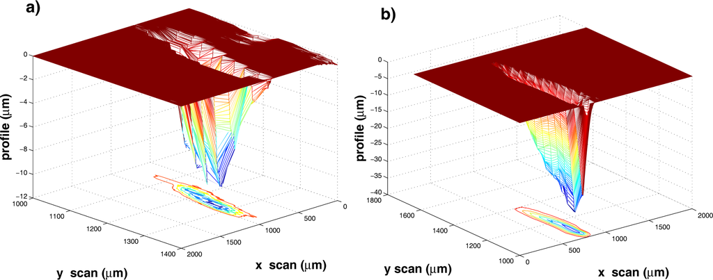
Figure 1.
3D representation of the craters produced on the surface of a silver target at 2.0 J·cm−2 by (a) 50 and (b) 200 laser pulses. At the bottom are the corresponding contour plots.
Considering the photo-thermal activation of the material removal in open air, the excitation energy from the laser propagates mainly within the target material due to the poor thermal contact between the target surface and the surrounding air: this results in the considerable depth of the craters as compared to their width. At higher N, the strong heating of the target surface combined with the instabilities arising within the melted layer at the target surface heated up to the critical temperature may produce a roughening of the crater surface that we observe experimentally. The presence of rims around the craters can be also explained by the strong temperature rise of the target surface that, in turn, leads to hot and dense ablation plasmas. The latter decouple from the liquefied target surface with a large acceleration oriented normal to it, thus exerting a strong recoil pressure onto the melted layer. Some data treatment was performed leading to the crater pictures in Figure 1: target surface leveling along the XY plane (see the flat area in Figure 1) and removal of any protruding features for which Z > 0. The volume of such redeposited and then melted material removed from the crater is subtracted from the total volume of the crater. The estimated crater volumes are reported in Table 1. We notice from Figure 2 that the number of laser shots and the ablated mass are linearly correlated with each other. The data were fitted to the linear relation M = mpN, M being the mass removed by N laser pulses. The results of the fit are reported in Table 1. In the considered case, about 60.0 ng, corresponding to about 3.35 × 10¹⁴ silver atoms, are removed from the target by a single laser pulse. With an estimated error for each volume value (taking into account the proper error on x, y and z measurements), less than 3%, the ultimate error on mp is about 5%, as evaluated from the fitting procedure. Determining mp is of critical relevance when the morphologies of samples deposited by PLD in the presence of an ambient gas are investigated. Film properties, as will be discussed in the next sections, sensitively depend on the interaction between the ablation plasma and ambient gas via the interplay of plasma mass m and gas density ρ.

Table 1.
Measurement of crater volume on an irradiated silver target. Data were fitted to the linear relation: M = mpN, M is the total mass removed; the mass and number of silver atoms ablated per single pulse are: mp = 60.0 ng and Nat = 3.35 × 10¹⁴ atoms, respectively.
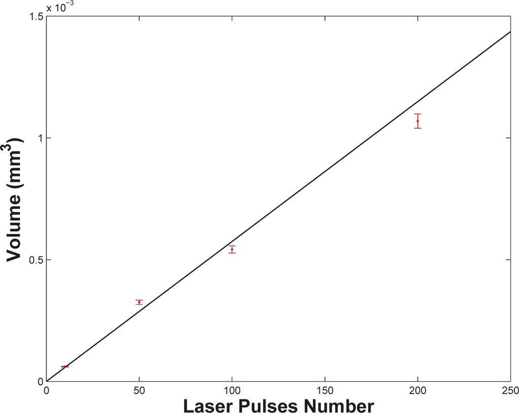
Figure 2.
Crater volumes on the surface of a silver target as a function of the laser shot number. The line is a linear fit to the data.
3.2. Surface Morphology
The optical properties of gold and silver nanostructured thin films are sensitively affected by their surface morphology. For isolated silver and gold NPs with a typical size ranging from a few nm up to 30 nm, the LSPR lies at about 400 and 520 nm, respectively. Moving to NP arrangements, self-organized or engineered at the nanoscale, both the position and the width of the LSPR peak depend on the size, shape, number density, mutual distance and aggregation features of the NPs [13]. The control of these properties then results in the control of the optical properties and, ultimately, of the SERS activity of the assembly. Among the several process parameters that affect the morphology of PLD synthesized films, two appear to play a major role: laser pulse number and gas pressure. While the first controls the degree of the NP number density and aggregation on the substrate, the latter mostly influences the interaction between plasma and ambient gas. In Figure 3, we show the surface of silver samples grown under identical conditions (F = 2.0 J·cm−2, Pg = 70 Pa of Ar, dT−S = 35 mm), but changing the laser pulse number between 1000 and 3 × 10⁴.
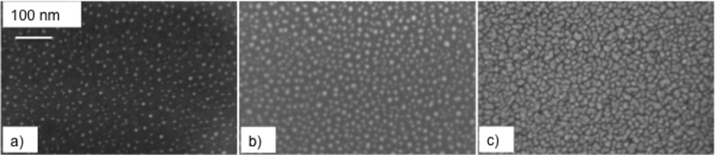
Figure 3.
SEM images of the surface morphology of silver samples deposited at 70 Pa of Ar with: (a) 1000, (b) 10,000, and (c) 3 × 10⁴ laser pulse.
We see that, at a low pulse number (see Figure 3a), the surface is covered by isolated, nearly spherical NPs. As N increases, the NP number density also increases, and deviations towards non-spherical geometry, with increasing NP size, are evident at some locations, together with incipient particle coalescence. Finally, at the highest N value (3 × 10⁴; see Figure 3c), the extensive coalescence among adjacent NPs occurs, thereby islands with an irregular shape and smooth edges form. Notably, such a surface morphology is characterized by the presence of inter-island channels with a defined average length and width. Couples or triplets of such channels meet together at junction points.
To the different morphologies correspond different optical properties of the films. The trend of the UV-Vis absorption spectra as a function of the different morphologies is shown in Figure 4. Increasing N, keeping fixed all other deposition parameters, a red-shift and a broadening of the FWHM of the LSPR peak is observed. A similar trend of change of the film surface morphology and, hence, of the optical properties of the film is observed if N is kept fixed, while the Ar pressure is changed. The effect of Ar pressure on film properties can be understood if the role of the gas on the expanding plasma is considered. Just after the end of the laser pulse, the ablated material starts to expand through the ambient gas, the expansion dynamics being driven by collisions: in the initial expansion stage, intra-plume collisions are dominant, but soon, collisions between plasma species and gas atoms become more and more effective. The collision rate depends on the gas density ρ and increases with ρ. The higher the collisional rate, the less the amount of material that reaches the substrate. At the same time, a higher collision rate promotes the formation and growth of NPs in the plasma. Such a complex process leads to the observed morphology dependence on N and on ambient gas density [14]. Thus, it is possible to tailor the optical properties of deposited films through the control of two easily adjustable deposition parameters (laser pulse number and Ar pressure), provided the relevant process parameters, in particular the laser fluence F, are kept fixed. The latter, given by the ratio of the laser pulse energy EL to the irradiated spot area A, can be kept fixed by changing appropriately both EL and A. Fixing F does not ensure that the ablated mass remains fixed as well. If we irradiate a larger area with a higher energy pulse, we can keep constant the fluence value, but a different mp value results. Referring to the above discussion, for expansions through an ambient gas, the interaction with gas atoms depends on the plasma mass. We have investigated this point growing a set of samples by changing mp, still keeping fixed F [15]. Two Ag samples were grown at 70 Pa of Ar, at dT−S = 35 mm, with 104 laser shots, F = 2.8 J·cm−2. To explore the role of mp, two focusing conditions were chosen, both corresponding to the same F value: E1 =10 mJ, A = 0.011 cm2 and E2 =30 mJ, A = 0.037 cm2. For the two conditions, different mp values result, namely mp1 = 7.0 ng and mp2 = 16.4 ng, as measured according to the procedure outlined in Section 3.1.
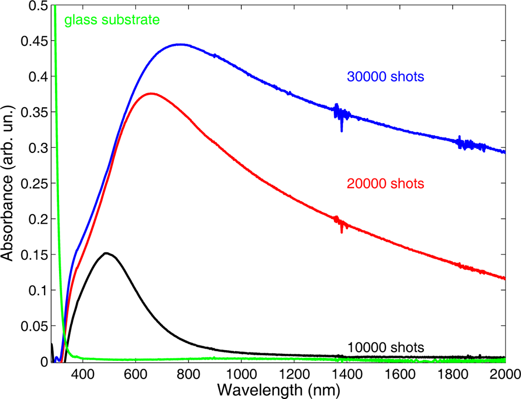
Figure 4.
UV-Vis absorption spectra of Ag samples deposited at 70 Pa of Ar with different numbers of laser shots.
In Figure 5 are shown the TEM pictures of the surface morphology of the two Ag films. The difference between the two morphologies is impressive. The surface of the sample deposited at lower mp1 (7.0 ng) is characterized by the presence both of small, nearly spherical NPs and of larger ones with the shape progressively more and more irregular, up to islands that result from the coalescence of several NPs. Looking at the surface of the sample deposited at higher mp2 (16.4 ng), we see a nearly percolated structure made of larger islands interconnected by a network of channels. In this sense, mp has the same effect on the evolution of sample surface morphology as lowering Ar pressure or increasing the laser pulse number. It is worth outlining that two well-differentiated surface morphologies were obtained adopting the same fluence. Thus, in a report on a PLD experiment, the fluence value is not enough to make it reproducible, if laser pulse energy EL and irradiated area A are not reported, as well, because these two parameters determine mp.
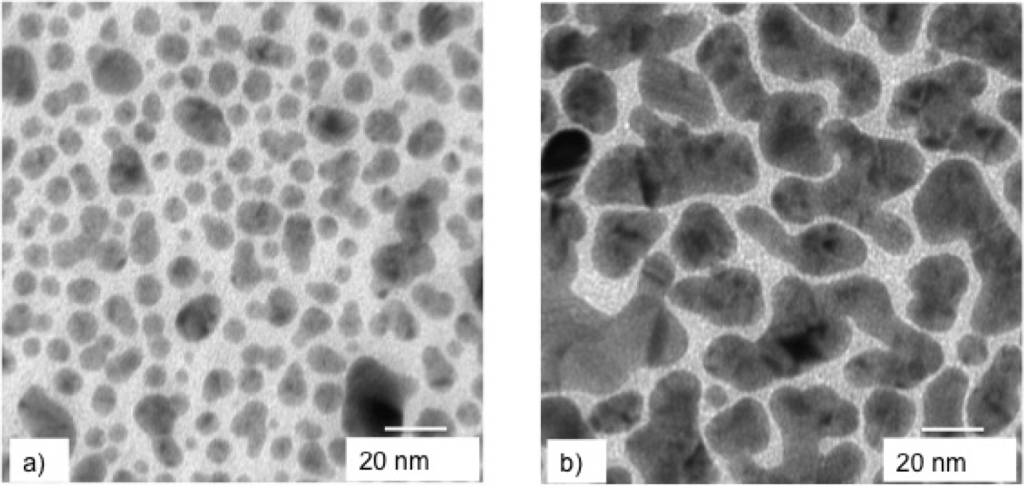
Figure 5.
TEM images of the surface morphologies of two Ag samples deposited at a laser fluence of 2.8 J·cm−2 with ablated mass per pulse of (a) 7.0 ng and (b) 16.4 ng.
In Figure 6a are displayed the UV-Vis absorption spectra of the above discussed samples. The different mp values lead to key differences in their optical properties.
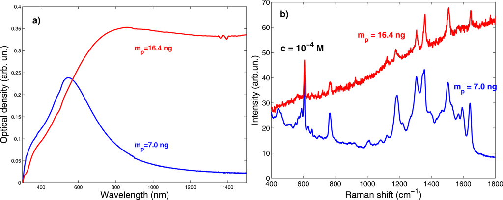
Figure 6.
(a) UV-Vis absorption spectra of Ag samples deposited at 70 Pa of Ar, 2.8 J cm−2, 104·laser shots and mp = 7.0 ng or mp = 16.4 ng. (b) Raman spectra acquired on the surface of the two samples soaked in an aqueous solution of rhodamine 6G (R6G) at a concentration c = 10−4 M.
We see that the LSPR considerably red-shifts and its FWHM increases, as expected once the morphology of the two samples is taken into account. Moreover, the large FWHM increase observed in the film deposited with the higher mp value (compare the film morphologies in Figure 5) points out the setting up of a composite system made of the metallic film and the supporting dielectric substrate (glass). In this system, the optical transitions are detuned via dipole-dipole interactions that broaden the LSPR peak [16,17].
The Raman spectra acquired on the surface of the two samples after being soaked for 1 h in an aqueous solution of rhodamine 6G (R6G) at a concentration of 10−4 M (Figure 6b) show a dramatic difference between the SERS response of the two films. The sample deposited at the lower mp1 shows a notably higher SERS efficiency. Thus, tuning the morphology and optical properties of nanostructured noble metal thin films is imperative to obtain highly SERS active substrates. Such a tuning cannot disregard detailed knowledge of the influence of all parameters on the deposition process, as exemplified by the study of the ablated mass per pulse.
3.3. SERS Activity of Pulsed Laser Ablated Silver and Gold Substrates
In this section, we report on some applications of Ag and Au SERS active substrates grown by PLD, whose properties were properly optimized from a parametric analysis [18,19]. We observed that Ag films deposited at 70 Pa of Ar, at F ≈ 2.0 J· cm−2 (A = 2 ÷ 3 × 10⁻³ cm2), dT−S = 35 mm, with 3 × 10⁴ laser shots show the best SERS activity, so far. Highly SERS active Au substrates were grown under identical conditions, but the Ar pressure was 100 Pa.
In Figure 7, we report the SERS spectra acquired on Ag and Au samples soaked in aqueous solutions of R6G, at the lowest concentrations we tested. The corresponding laser excitations were 632.8 nm for Ag and 785 nm for Au to achieve the maximum EF by matching the corresponding SPR absorption peak positions, observed near 550 and 800 nm, respectively [20,21].
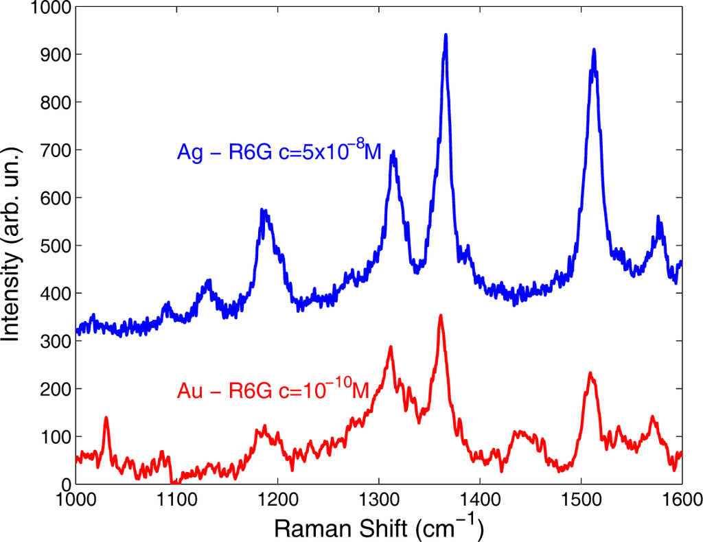
Figure 7.
Raman spectra acquired on silver and gold nanostructured substrates soaked in aqueous solutions of R6G at concentrations c = 5 × 10⁻⁸ and c = 10−10 M respectively.
The R6G peaks lying at 1189, 1314, 1366 and 1513 cm−1 assigned to the stretching modes of aromatic C bonds are clearly visible. Typical integration times varied between a few seconds and 240 s, pointing out that detection might be possible for this reference analyte at even lower concentration levels.
We believe that the detection at such a low concentration level is due to the formation of hot spots, whose number density strictly depends on film surface morphology, in turn controlled by an easily accessible deposition parameter, i.e., the laser pulse number (see Figure 2.). It is noteworthy that compared to other deposition methods, like thermal evaporation and sputtering, PLD allows synthesizing films without any post-deposition thermal treatment. Moreover, the process is performed at room temperature, thus making it possible to use every kind of substrate material. Finally, PLD is a physical deposition technique that does not require any chemical precursor, different from routes based on the chemical reduction of silver and gold salts to obtain NPs: these have undesired chemical residuals, often introducing disturbing features in SERS spectra.
The observed SERS enhancement was so high, since we choose the excitation wavelength (632.8 nm), such that the surface plasmon absorption band (see Figure 4) lies between the wavelengths of the exciting and the Raman scattered light; indeed, according to the electromagnetic theory, the optical properties of the metallic NPs set the choice of the excitation wavelength in SERS.
Raman spectroscopy is one of the most employed techniques in the cultural heritage field. Identification of dyes is a relevant issue in the field from the historical, conservation and restoration view points. Raman scattering presents some advantages with respect to other techniques, like X-ray fluorescence, UV-Vis absorption and Fourier transform infrared spectroscopy. The most relevant are its non-destructive character and its selectivity. With the advent of portable Raman microscopy apparatuses, measurements can be performed in situ on micrometer-sized areas of the artwork. SERS applied to this kind of investigation opens the way to the detection of exiguous amounts of substances employed in the realization of the work of art [22]. In Figure 8, we report as an example SERS measurements performed on a silver substrate soaked in a 10−4 M concentrated aqueous solution of alizarine. Alizarine, with its hydrolyzed counterpart, purpurine, are the two chromophores that characterize the organic garanza lake dye extracted from the root of the Rubia tinctorium plant. Red lake has been used since ancient Egyptian times until today. Its detection and the relative concentration of the two chromophores can allow identifying the origin and authenticity of the work of art or the presence of restoration works.
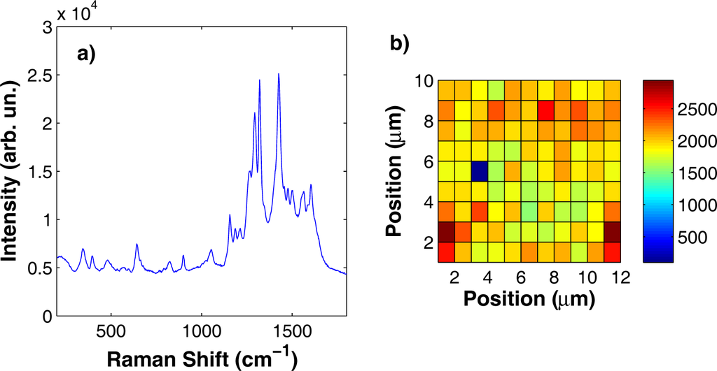
Figure 8.
(a) SERS spectrum acquired on a silver substrate soaked in an aqueous solution of alizarine at a concentration c = 10−4 M. (b) Intensity of the Raman peak at 900 cm−1 as a function of the position on the substrate surface over an area of 10 × 12 μm2. Detection point spacing, 1 μm.
All the alizarine Raman features were detected at 658, 823, 900, 1065, 1156, 1186, 1211, 1269, 1293, 1320, and 1425 cm−1. One of the most important requirements for a SERS substrate is the spatial homogeneity; indeed, Raman spectra should be reproducible over micron-sized areas with intensity variations within 20%. In Figure 8b, we report the results of a Raman mapping experiment performed over an area of 10 × 12 μm2 on an Ag substrate soaked in an aqueous solution of alizarine at a 10−4 M concentration. Raman spectra were acquired with a spatial resolution of about 1 μm, both along x and along y. In the Raman map (see Figure 8b), we report the intensity of the Raman peak at 900 cm−1 as a function of the position. We chose this peak because it is well separated from other alizarine features, thus making it easier to evaluate its intensity over the background. The mean intensity of the peak was of 2003 counts with a standard deviation of 318 counts, corresponding to a variation of about 15%. A companion experiment was performed on a gold substrate soaked in a purpurine aqueous solution at the same 10−4 M concentration. The results are reported in Figure 9. Purpurine Raman features are located at 620, 650, 820, 904, 970, 1065, 1313, 1440 and 1470 cm−1. The investigated area to test the substrate spatial homogeneity was 10 × 8 μm2 and the intensity fluctuations of the peak at 1065 cm−1 as a function of the position on the considered surface was about 11% of the average peak value.
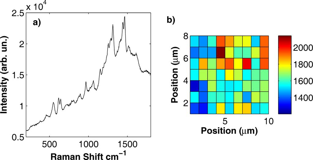
Figure 9.
(a) SERS spectrum acquired on a silver substrate soaked in an aqueous solution of purpurine at a concentration c = 10−4 M; (b) intensity of the Raman peak at 1065 cm−1 as a function of the position on the substrate surface over an area of 10 × 8 μm2. Detection point spacing, 1 μm.
4. Conclusions
In conclusion, nanosecond laser ablation in an inert gas atmosphere at high pressure allows depositing NP arrays of noble metals with a finely controlled nanostructure. By such a kind of bottom-up laser nano-machining, metallic substrates with optical properties tailored ad hoc were prepared and utilized for the selective recognition of analytes in a small concentration via surface-enhanced Raman spectroscopy.
Acknowledgments
Matteo Tommasini and Paolo Maria Ossi acknowledge support from Polisocial Award 2014, Project “Controllare l’epilessia nei Paesi in via di sviluppo” (Controlling epilepsy in Developing Countries).
Author Contributions
Fortunato Neri, Sebastiano Trusso and Paolo Maria Ossi conceived and designed the experiments; Enza Fazio, Rosina C. Ponterio and Sebastiano Trusso performed the experiments; Enza Fazio and Rosina C. Ponterio analyzed the data; Fortunato Neri and Matteo Tommasini contributed reagents/materials/analysis tools; Sebastiano Trusso and Paolo Maria Ossi wrote the paper.
Conflicts of Interest
The authors declare no conflict of interest.
References
- Srinivasan, R.; Sutcliffe, E.; Braren, B. Ablation and etching of polymethylmethacrylate by very short laser pulses. Appl. Phys. Lett 1987, 51, 1285–1287. [Google Scholar]
- Bärsch, N.; Körber, K.; Ostendorf, A.; Tönshoff, K.H. Ablation and cutting of planar silicon devices using femtosecond laser pulses. Appl. Phys. A 2003, 7, 237–242. [Google Scholar]
- Küper, S.; Stuke, M. Ablation of polytetrafluoroethylene (Teflon) with femtosecond UV excimer laser pulses. Appl. Phys. Lett 1989, 54, 4–6. [Google Scholar]
- Davis, K.M.; Miura, K.; Sugimoto, N.; Hirao, K. Writing waveguides in glass with a femtosecond laser. Opt. Lett 1996, 21, 1729–1731. [Google Scholar]
- Kawata, S.; Sun, H.B.; Tanaka, T.; Takada, K. Finer features for functional microdevices. Nature 2001, 412, 697–698. [Google Scholar]
- Reif, J.; Varlamova, O.; Uhlig, S.; Varlamov, S.; Bestehorn, M. On the physics of self-organized nanostructure formation upon femtosecond laser ablation. Appl. Phys. A 2014, 117, 179–184. [Google Scholar]
- Carey, J.E.; Crouch, C.H.; Shen, M.; Mazur, E. Visible and near-infrared responsivity of femtosecond-laser microstructured silicon photodiodes. Opt. Lett 2005, 30, 1773–1775. [Google Scholar]
- Sugioka, K. Ultrafast Laser Micro- and Nano-processing of Glasses. In Lasers in Materials Science; Castillejo, M., Ossi, P.M., Zhigilei, L.V., Eds.; Springer: Berlin, Germany, 2014; pp. 359–380. [Google Scholar]
- Nöel, S.; Hermann, J.; Itina, T. Investigation of nanoparticle generation during femtosecond laser ablation of metals. Appl. Surf. Sci 2007, 253, 6310–6315. [Google Scholar]
- García-Vidal, F.J.; Pendry, J.B. Collective Theory for Surface Enhanced Raman Scattering. Phys. Rev. Lett 1996, 77, 1163–1166. [Google Scholar]
- Nie, S.; Emory, S.R. Probing Single Molecules and Single Nanoparticles by Surface-Enhanced Raman Scattering. Science 1997, 275, 1102. [Google Scholar]
- Halas, N.J.; Moskovits, M. Surface-enhanced Raman spectroscopy: Substrates and materials for research and applications. MRS Bull 2013, 38, 607–611. [Google Scholar]
- Mulvaney, P. Surface plasmon spectroscopy of nanosized metal particles. Langmuir 1996, 12, 788–800. [Google Scholar]
- Bailini, A.; Ossi, P.M.; Rivolta, A. Plume propagation through a buffer gas and cluster prediction. Appl. Surf. Sci 2007, 253, 7682–7685. [Google Scholar]
- Spadaro, M.C.; Fazio, E.; Neri, F.; Ossi, P.M.; Trusso, S. On the influence of the mass ablated by a laser pulse on thin film morphology and optical properties. Appl. Phys. A 2014, 117, 137–142. [Google Scholar]
- Shalaev, V. Electromagnetic properties of small particle composites. Phys. Rep 1996, 272, 61–137. [Google Scholar]
- Micali, N.; Neri, F.; Ossi, P.M.; Trusso, S. Light scattering enhancement in nanostructured silver thin film composites. J. Phys. Chem. C 2013, 117, 3497–3502. [Google Scholar]
- D’Andrea, C.; Neri, F.; Ossi, P.M.; Santo, N.; Trusso, S. The controlled pulsed laser deposition of Ag nanoparticle arrays for surface enhanced Raman scattering. Nanotechnology 2009, 20, 245606. [Google Scholar]
- Fazio, E.; Neri, F.; D’Andrea, C.; Ossi, P.M.; Santo, N.; Trusso, S. SERS activity of pulsed laser ablated silver thin films with controlled nanostructure. J. Raman Spectrosc 2011, 42, 1298–1304. [Google Scholar]
- Agarwal, N.R.; Fazio, E.; Neri, F.; Trusso, S.; Castiglioni, C.; Lucotti, A.; Santo, N.; Ossi, P.M. Ag and Au nanoparticles for SERS substrates produced by pulsed laser ablation. Cryst. Res. Technol 2011, 46, 836–840. [Google Scholar]
- Merlen, A.; Gadenne, V.; Romann, J.; Chevallier, V.; Patrone, L.; Valmalette, J.C. Surface enhanced Raman spectroscopy of organic molecules deposited on gold sputtered substrates. Nanotechnology 2009, 20, 215705. [Google Scholar]
- Leona, M. Microanalysis of organic pigments and glazes in polychrome works of art by surface-enhanced resonance Raman scattering. Proc. Natl. Acad. Sci. USA 2009, 106, 14757–14762. [Google Scholar]
© 2014 by the authors; licensee MDPI, Basel, Switzerland This article is an open access article distributed under the terms and conditions of the Creative Commons Attribution license (http://creativecommons.org/licenses/by/4.0/).