Abstract
We report in this paper a novel, inexpensive and flexible method for fabricating micrometer- and nanometer-scale three-dimensional (3D) polymer structures using visible light sources instead of ultra-violet (UV) light sources or lasers. This method also does not require the conventional micro-photolithographic technique (i.e., photolithographic masks) for patterning and fabricating polymer structures such as hydrogels. The major materials and methods required for this novel fabrication technology are: (1) any cross-linked network of photoactive polymers (examples of fabricated poly(ethylene glycol) (PEG)-diacrylate hydrogel structures are shown in this paper); (2) an Optically-induced Dielectrophoresis (ODEP) System which includes an “ODEP chip” (i.e., any chip that changes its surface conductivity when exposed to visible light), an optical microscope, a projector, and a computer; and (3) an animator software hosted on a computer that can generate virtual or dynamic patterns which can be projected onto the “ODEP chip” through the use of a projector and a condenser lens. Essentially, by placing a photosensitive polymer solution inside the microfluidic platform formed by the “ODEP chip” bonded to another substrate, and applying an alternating current (a.c.) electrical potential across the polymer solution (typically ∼20 Vp-p at 10 kHz), solid polymer micro/nano structures can then be formed on the “ODEP chip” surface when visible-light is projected onto the chip. The 2D lateral geometry (x and y dimensions) and the thickness (height) of the micro/nano structures are dictated by the image geometry of the visible light projected onto the “ODEP chip” and also the time duration of projection. Typically, after an image projection with intensity ranging from ∼0.2 to 0.4 mW/cm2 for 10 s, ∼200 nm high structures can be formed. In our current system, the thickness of these polymer structures can be controlled to form from ∼200 nanometers to ∼3 micrometers structures. However, in the in-plane dimensions, only ∼7 μm resolution can be achieved now, due to the optical diffraction limit and the physical dimensions of DMD mirrors in the projector. Nevertheless, with higher quality optical components, the in-plane resolution is expected to be sub-micron.1. Introduction
Three-dimensional cross-linked hydrogel structures with controlled shapes and sizes at the microscale have significant potential to generate tissue engineering constructs that mimic native tissue architecture and for guiding cellular differentiation and organization [1]. In recent years, surface micropatterning technologies including photopatterning, soft lithographic techniques, scanning electrochemical microscope and scanning-probe-lithography have significantly enhanced the ability to tailor cell microenvironment and control the surface chemistry and topography at the micrometer level [2-8]. More recently, multiphoton lithography (MPL) has been reported for rapidly printing three-dimensional microscopic replicas and biological architectures [9,10]. Besides using photopolymerization processes to form hydrogel patterns as mentioned above, electrochemically triggered polymerization has also been reported to “write” hydrogel patterns by using a small oxygen bubble as the pen nib [11-13]. However, this method limits the ability to pattern structures at the microscale level due to the large size of generated bubbles (∼20 μm).
Here, we describe our recent invention of using Optically-induced Dielectrophoresis (ODEP) as a simple, versatile, and inexpensive technique to directly assemble polymers (e.g., (poly(ethylene glycol) (PEG)-diacrylate) hydrogels (PEDGA)) to form 3D structures with controlled shapes and sizes down to nanometer-scale. Since dielectrophoretic nanoscale manipulation are known to also contain other phenomena, such as electro-osmosis and interfacial double-layers, etc., we use the term “electrokinetic forces” to describe all the possible forces at play during the optically-induced dielectrophoresis process. Although the approach presented here can be generalized to other polymer systems (e.g., photopolymerizaed acrylates) using appropriate sensitizers, in this paper we present only the results for PEGDA hydrogels. Essentially, by applying ODEP force (and possibly other eletrokinetic forces) on polymer solutions in a microfluidic system, three-dimensional polymer structures with controlled shapes and sizes can be generated. The sizes and shapes of the polymer structures are dictated by the optical images projected onto the “ODEP chip”, i.e., typical projectors can be used to project computer-generated images onto an “ODEP chip” through a custom-built microscope system. The relationship between the thicknesses of hydrogel structures and visible-light exposure duration time is also characterized.
2. Theoretical Background of ODEP
2.1. Optically Induced Dielectrophoresis
Dielectrophoresis is a phenomenon in which a force is exerted on a dielectric particle when it is subjected to a non-uniform electric field. The time-average DEP force exerted on particles can be described as [14]:
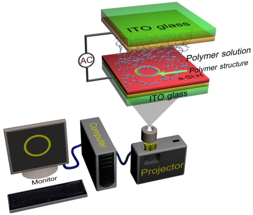
On the other hand, for an “ODEP chip” (as shown in Figure 1), when an a.c. bias voltage is applied across the top and the bottom ITO electrodes, a small electric potential drops across the liquid layer, and an uniform electric field is produced in the liquid layer. (In this paper, an “ODEP chip” is defined as a microfluidic chip with the bottom substrate made from an ITO glass coated with an a-Si:H layer; the top substrate is an ITO glass. The top and bottom substrates are separated by a PDMS spacer or a double-sided tape to create a microfluidic channel into which the polymer solutions are injected). That is, with no incident light illuminating the a-Si:H thin film layer of the ODEP chip, the thin film layer has a high electrical impedance and behaves as an insulator. When an incident light beam illuminates the a-Si:H layer, the conductivity of the illuminated region of this layer is sharply increased by several magnitudes due to the photogenerated electron-holes. Thus, most of the applied voltage between the top and bottom ITO electrodes is shifted to the liquid layer, and the illuminated light pattern on the a-Si:H becomes effectively a localized virtual electrode and generates a non-uniform electric field. This optically induced non-uniform electric field generates a DEP force around objects in the field, which is termed as ODEP force. The ODEP force is either positive (objects are attracted to the maximum of electric field gradient) or negative (objects are repelled from the maximum of the electric field gradient), depending on the dielectric properties of the objects, the liquid media, and frequency of applied a.c. voltage.
2.2. Optoelectrically Induced Polymerization
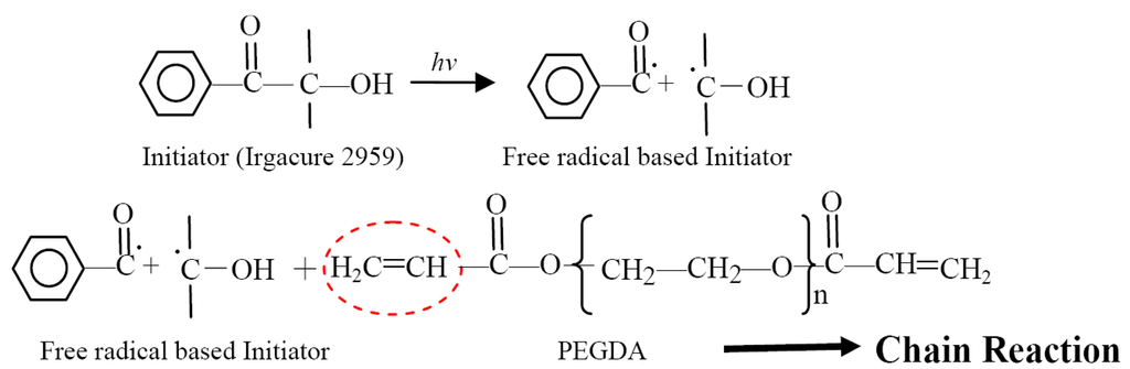
Poly (ethylene glycol) diacrylate (PEGDA), a biocompatible and water-soluble polymer, can be cross-linked with an initiator (such as Irgacure 2959, (1-[4-(2-Hydroxyethoxy)-phenyl]-2-hydroxy-2-methyl-1-propane-1-one)) to form a three-dimensional polymer network. The process of PEGDA chain reaction with a photoinitiator is shown in Figure 2 below. Two typical free-radical chain polymerization methods are UV light-induced photopolymerization and electrochemical-induced polymerization. In this paper, we present an optoelectrically induced polymerization technique for patterning PEGDA hydrogels. The entire polymerization process can be explained by two steps: cross-linking process and patterning process. Initially, the initiator molecules and stable precursor molecules in solution will not react with each another. When visible light with wavelengths between 390 nm and 770 nm generated by a commercial projector is illuminated onto the prepared solution, the generated photon energy can be approximately calculated from the classical physical formula: E = h·c/λ, where E is the generated energy and has a range of 1.61 to 3.17 eV, respectively for 390 nm and 770 nm light source; h is the Planck s constant (4.13 × 10⁻¹⁵ eV·s), c is the speed of light (3 × 10⁻⁸ m/s) and λ is the wavelength of light. Although the bond energy of C-C bonds in an organic molecule is typically assumed to be 3–5 eV, the bombardment energy for C-C bond cleavage is raised to 15–50 eV [15], thus the photon energy generated by visible light is not sufficient for C-C bond cleavage. This indicates that the precursor molecules are not cross-linked with the initiator molecules at this step. However, when an a.c. bias with a magnitude of 20 Vp-p and frequency of 10 kHz is applied across the ODEP chip, a non-uniform electric field is generated and the transient energy that can be consumed is estimated to be ∼20 eV, which is sufficient for the C-C bond cleavage.(The estimated value of 20 eV is based on the definition of “elctronvolt”, i.e., it is defined as the amount of kinetic energy gained by a single unbound electron when it accelerates through an electric potential difference of one volt. Hence, the kinetic energy generated by an electron when it accelerates through an electric potential of 20 Volt is 20 eV). Hence, the initiator molecule is cleaved to produce free-radical molecules and these reactive molecules can then be attracted with a monomer molecule by opening its double-bond, which produce a new radical center on the monomer molecule. After cross-linking with the photoinitiator, the hydrogels are formed at specific locations on the ODEP chip due to the induced positive ODEP forces generated by projected light patterns. In the whole process, the optical image with different shapes and sizes serve as “virtual electrodes” to induce non-uniform electric field and “virtual masks” to generate hydrogel structures. Hence, the a.c. electrical potential input combined with the optical light can be utilized to induce polymerization for cross-linking hydrogels and then subsequently pattern the PEGDA hydrogels, respectively.
3. Experimental Methods
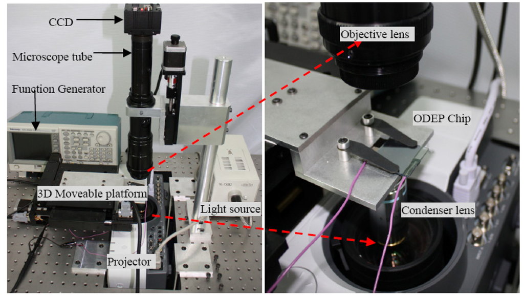
A photograph of the actual experimental “ODEP System” is shown in Figure 3 below. As explained earlier, the “ODEP chip” consists of a layer of photoconductive material on an indium tin oxide (ITO)-coated glass substrate. Liquid containing the particles of interest is sandwiched between this lower device and a top piece of ITO-coated glass. An a.c. bias is applied across the two ITO layers. Initially, the majority of the a.c. bias drops across amorphous silicon layer due to its high electrical impedance in the absence of light. However, upon an optical image illumination, the amorphous silicon layer's conductivity is increased by several orders of magnitude due to the generated electron-holes pairs. As a result, a localized non-uniform electric field is generated above the illuminated region in the liquid layer. The polymers in the medium thus experience an attractive or repulsive DEP force due to the induced electric dipoles. Here, the projected optical patterns designed by an animator software function as microelectrodes to induce non-uniform electric field, thus they are referred to “virtual” or “dynamic” electrodes in the “ODEP chip”. These “virtual electrodes” in the “ODEP System” can be generated by Digital Mirror Device (DMD) or LCD panels which are illuminated by visible-light sources such as a halogen lamp or a LED lamp.
3.1. ODEP Chip Fabrication
We have shown the following process for fabricating an “ODEP chip” which provides consistent results for fabricating the micro/nano polymer structures described in this paper. However, any other methods or materials could also be used to produce an “ODEP chip”, i.e., provided that a chip could generate a non-uniform electrical field when visible-light is projected on to it, then the chip can be used in the “ODEP System” as described in this application.
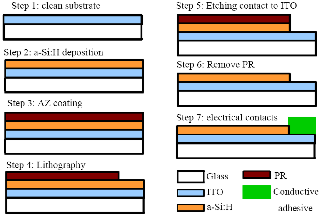
The “ODEP chip” can be fabricated using traditional MEMS fabricating processes as shown in Figure 4 below. The process starts with a 1.1-mm thick glass coated with 120 nm layer of sputtered indium tin oxide (ITO), with 15 Ω/□ sheet resistances. The ITO glass should first be cleaned by alcohol, ultrapure water and then N2 dried. Then, a 1 μm hydrogenated amorphous silicon layer (a-Si:H) is deposited onto the ITO layer using plasma-enhanced chemical vapor deposition (PECVD) process. After the a-Si:H deposition is completed, the glass are diced to make ODEP chips with typical size of 3 cm × 3 cm. Then, a lithographic plus etching process should be used to remove part of the a-Si:H so that part of the ITO film is exposed and be used as a conductive electrode (Steps 3 to 6 in Figure 4). In addition, the top side of the “ODEP chip” should consist of another ITO-coated glass slide with the same size of 3 cm × 3 cm. (The top side ITO layer should eventually be connected to the bottom side ITO layer through the application of an a.c. voltage potential as illustrated in Figure 2).
4. Examples of Micro/Nano Structures Fabricated by ODEP System
This section shows several examples of fabricated hydrogel structures. Hydrogel is only one of many possible materials that can be used to fabricate micro/nano structures using the “ODEP System” described here. Below is a suggested preparatory process for the polymer solution used for the “ODEP System”.
Hydrogel preparation: Poly (ethylene) glycol (PEGDA) (Sigma Aldrich) is dissolved in DI water to form PEGDA concentration of 20% v/v. The photoinitiator solution is prepared by completely dissolving 2-dimethoxy-2-phenyl-acetophenone (Irgacure 2959) (Sigma Aldrich) in DI water to form the photoinitiator concentration of 0.2% w/v. Then, the photoinitiator solution is mixed with PEGDA solution with the ratio of 1:1. Then, the mixed solution is sonicated for 15 min.
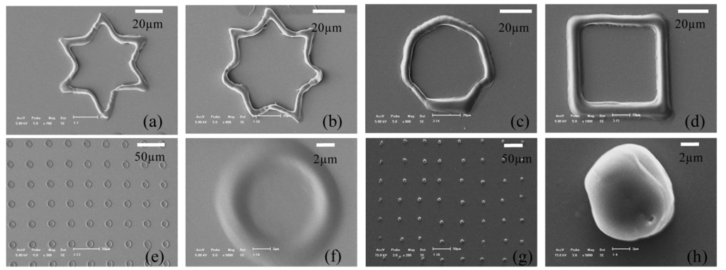
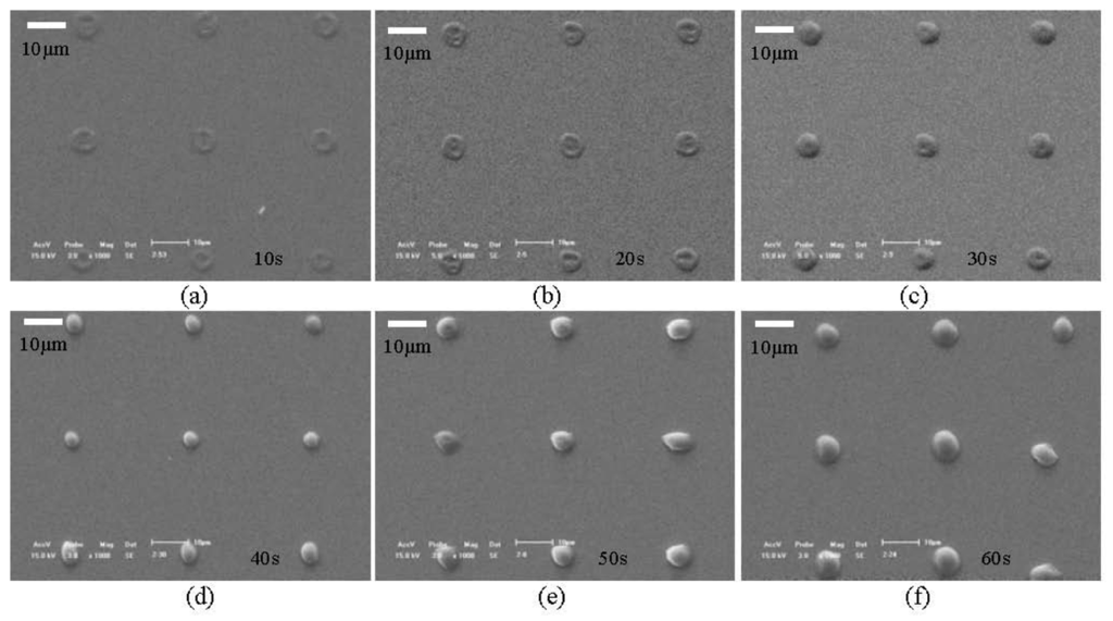
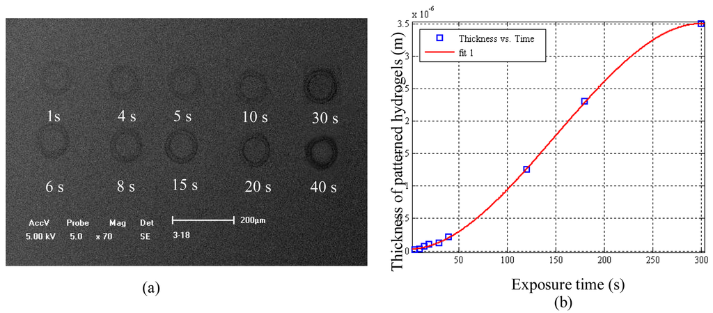
Figure 5(a-d) shows SEM (scanning electron microscope) images of geometric structures formed by the hydrogel solution described above using the “ODEP System” described in this paper. Figure 6(a-f) shows the SEM images of patterned structures (all with a “spot” as the projected image) with different depositing time, from 10 to 60 s, with an interval of 10 s. Figure 7 shows a plot of the relationship between thickness of hydrogel structure and exposure time with the exposure intensity of 1.1 mW/cm2.
5. Discussion
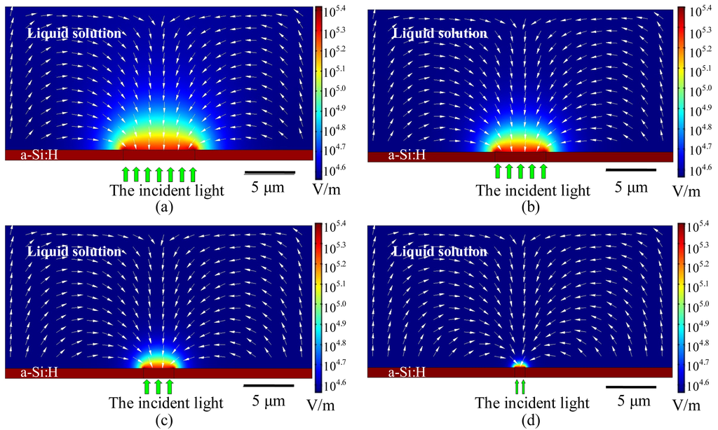
In order to explain the principle of formation of PEGDA structures, numerical simulations were performed to analyze the optically-induced DEP force close to the surface of the bottom substrate of the “ODEP chip”. Using an axi-symmetic 2D model, and assuming a light spot with a diameter of 7 μm (which was the geometry of the light pattern used to generate the structures shown in Figure 6), the distribution of the electric field in the proximity of the illuminated optical pattern on the bottom substrate can be calculated. In the numerical analysis, the following parameters were used: conductivity of the PEGDA solution is 1 × 10⁻³ S/m; conductivity of the amorphous silicon with incident light is 1 × 10⁻⁵ S/m; and the dark conductivity of the amorphous silicon is 1 × 10⁻¹¹ S/m (these data were measured using the Keithley 2,410 Source Meter). The numerical results of the ODEP force can be obtained by finite element method utilizing Comsol Multiphysics 3.5a (a commercial finite element simulation tool), which provides a time-harmonic analysis module with quasi-static currents field (with 2D axial symmetry) that can be used to solve the Maxwell's equations in the subdomain of the fluidic medium in the “ODEP chip”. The simulation module and its corresponding boundary settings are the same as the ones used in our prior work as described in [17]. The result of the electric field strength is shown in Figure 8(a) for an optical spot size of 7 μm. As shown, the field strength is the highest near the edge of the “spot” pattern, and hence hydrogel molecules accumulate near the edge of the spot and formed ring-like structures as shown in Figure 6(a-c). However, as soon as the ring-like structures are formed on the a-Si:H surface, the polymer structure block off part of the projected optical pattern, so the spot size is effectively decreased, and the virtual electrode on the a-Si:H layer is consequently reduced in size. Hence, as time progresses, the effective size of the virtual electrode shrinks as polymers are attracted by optically-induced DEP force into the center of illuminated optical spot. Figure 8(a-d) shows simulation results of the effectively decreased spot size, indicating that the electric field strength and DEP force vectors will evolve as a function of the optical spot size and thus result in polymer structures as shown in Figure 6(d-f).
6. Conclusion
We have invented a new, simple, inexpensive, and flexible technique to fabricate polymer structures by using an optoelectronically-induced dielectrophoretic platform. As an example, three-dimensional cross-linked PEDGA hydrogel structures with controllable shapes and sizes at the microscale (∼7 μm in-plane resolution) with controllable nanoscale thickness (∼200 nm height) have been successfully fabricated on chips using optical image patterns, which are projected from a commercial projector and a condenser lens directly onto the chip. Experimental results also demonstrate that parallel patterning of hydrogel structures can be achieved by using this new fabrication technique, and the thickness of hydrogel structures fabricated is proportional to the image-exposure time duration.
Acknowledgments
The present work is supported by a self-sponsored project of the State Key Laboratory of Robotics (No. 2009Z02). This project is also partially supported by the CAS/SAFEA International Partnership Program for Creative Research Teams. Wen J. Li would like to thank the City University of Hong Kong's start-up fund for supporting this project, and also thank The Chinese University of Hong Kong for its continual support of his graduate students there. All authors thank all members in the Micro/Nano Automation Group of the State Key Laboratory of Robotics, SIA, CAS, for their valuable discussions and support.
References
- Polizzotti, B.D.; Fairbanks, B.D.; Anseth, K.S. Three-dimensional biochemical patterning of click-based composite hydrogels via thiolene photopolymerization. Biomacromolecules 2008, 9, 1084–1087. [Google Scholar]
- Koh, W.G.; Itle, L.J.; Pishko, M.V. Molding of hydrogel multipheno type cell microstructures to create microarrays. Anal. Chem. 2003, 75, 5783–5792. [Google Scholar]
- Liu, V.A.; Bhatia, S.N. Three-dimensional photopatterning of hydrogels containing living cells. Biomed. Microdev. 2002, 4, 257–266. [Google Scholar]
- Koh, W.G.; Revzin, A.; Pishko, M.V. Poly(ethylene glycol) hydrogel microstructures encapsulating living cells. Langmuir 2002, 18, 2459–2462. [Google Scholar]
- Tang, M.D.; Golden, A.P.; Tien, J. Molding of three-dimensional microstructures of gels. J. Am. Chem. Soc. 2003, 125, 12988–12989. [Google Scholar]
- Franzesi, G.T.; Ni, B.; Ling, Y.; Khademhosseini, A. A controlled-release strategy for the generation of cross-linked hydrogel microstructures. J. Am. Chem. Soc. 2006, 128, 15064–15065. [Google Scholar]
- Nie, Z.; Kumacheva, E. Patterning surfaces with functional polymers. Nature Mater. 2008, 7, 277–290. [Google Scholar]
- Beebe, D.J.; Moore, J.S.; Bauer, J.M.; Yu, Q.; Liu, R.H.; Devadoss, C.; Jo, B.H. Functional hydrogel structures for autonomous flow control inside microfluidic channels. Nature 2000, 404, 588–590. [Google Scholar]
- Nielson, R.; Kaehr, B.; Shear, J.B. Microreplication and design of biological architectures using dynamic‐mask multiphoton lithography. Small 2009, 5, 120–125. [Google Scholar]
- Khripin, Y.; Pristinski, D.; Dunphy, D.R.; Brinker, C.J.; Kaehr, B. Protein-directed assembly of arbitrary three-dimensional nanoporous silica architectures. ACS Nano 2011, 5, 1401–1409. [Google Scholar]
- Reuber, J.; Reinhardt, H.; Johannsmann, D. Formation of surface-attached responsive gel layers via electrochemically induced free-radical polymerization. Langmuir 2006, 22, 3362–3367. [Google Scholar]
- Bünsow, J.; Johannsmann, D. Patterned hydrogel layers produced by electrochemically triggered polymerization. Macromol. Rapid Commun. 2009, 30, 858–863. [Google Scholar]
- Bünsow, J.; Manz, M.; Vana, P.; Johannsmann, D. Electrochemically induced RAFT polymerization of thermoresponsive hydrogel films: Impact on film thickness and surface morphology. Macromol. Chem. Phys. 2010, 211, 761–767. [Google Scholar]
- Jone, T.B. Electromechanics of Particles; Cambridge University Press: New York, NY, USA, 1995; pp. 17–20. [Google Scholar]
- Lau, W.M.; Zheng, Z.; Wang, Y.H.; Luo, Y.; Xi, L.; Wong, K.W.; Wong, K.Y. Cross-linking organic semiconducting molecules by preferential CH cleavage via chemistry with a tiny hammer. Can. J. Chem. 2007, 85, 859–865. [Google Scholar]
- Wang, S.E.; Li, M.L.; Qu, Y.L.; Dong, Z.L.; Li, W.J. Comparing ODEP and DEP Forces for Micro/Nano Scale Manipulation: A Theoretical Analysis. Proceedings of the 5th IEEE International Conference on Nano/Micro Engineered and Molecular Systems (IEEE-NEMS 2010), Xiamen, China, 20–23 January 2010; pp. 1174–1179.
- Liang, W.F.; Wang, S.E.; Qu, Y.L.; Dong, Z.L.; Lee, G.B.; Li, W.J. An Equivalent Electrical Model for Numerical Analyses of ODEP Manipulation. Proceedings of the 6th IEEE International Conference on Nano/Micro Engineered and Molecular Systems (IEEE-NEMS 2011), Kaohsiung, Taiwan, 20–23 February 2011; pp. 860–865.
© 2011 by the authors; licensee MDPI, Basel, Switzerland. This article is an open access article distributed under the terms and conditions of the Creative Commons Attribution license (http://creativecommons.org/licenses/by/3.0/).