Self-Assembly of Microscale Parts through Magnetic and Capillary Interactions
Abstract
: Self-assembly is a promising technique to overcome fundamental limitations with integrating, packaging, and general handling of individual electronic-related components with characteristic lengths significantly smaller than 1 mm. Here we describe the use of magnetic and capillary forces to self-assemble 280 μm sized silicon building blocks into interconnected structures which approach a three-dimensional crystalline configuration. Integrated permanent magnet microstructures provided magnetic forces, while a low-melting-point solder alloy provided capillary forces. A finite element model of forces between the magnetic features demonstrated the utility of magnetic forces at this size scale. Despite a slight departure from designed dimensions in the actual fabricated parts, the combination of magnetic and capillary forces improved the assembly yield to 8%, over approximately 0.1% achieved previously with capillary forces alone.1. Introduction
The manufacture of microsystems by assembling pre-microfabricated parts in different ways may enable many new applications in sensing, microrobotics, and even high performance computing. By working with pre-microfabricated parts, the investment required for the customization of wafer-scale manufacturing processes may be minimized. Self-assembly has been studied as a way to enable these advantages through the handling, packaging, and integration of parts to create two or three dimensional structures in a highly parallel and scalable manner [1]. Self-assembly is particularly applicable for parts or components having length scales below 0.5 mm [2], because the number of parts needed to create useful structures or systems may be very large, and conventional pick and place or other serial assembly methods become infeasible. In addition, manual or robotic pick and place methods become increasingly difficult as surface forces become dominant at shorter length scales. Self-assembly aims to take advantage of these dominant forces by directing a collection of parts toward desired binding sites and in desired orientations.
Capillary forces resulting from one or more immiscible fluids represent one useful set of phenomenon to exploit for directing fluidic self-assembly. These forces may arise from insoluble polymers [3-5], non-polar liquids [6], liquid solders [7-12], gas-liquid interfaces [13], or a hierarchical combination of these techniques [14]. These methods are competitive with and produce similarly high yields as other approaches to parallel heterogeneous integration, such as parallel pick and place techniques based on elastomeric stamps [15-18]. In addition to these examples of assembly on templates which essentially approach a two-dimensional plane at the point of each binding site, binding sites may also be on the microscale components themselves to create three dimensional material or device structures [19-23]. One problem with capillary forces is that they only act over very short distances—a part must generally be in contact with its intended binding site in order for capillary forces to align and complete the assembly.
Magnetic forces are also useful to assemble parts at magnetized template sites [24-27], to manipulate ferromagnetic parts by external fields [28-30], and to assemble magnetized parts with one another [27,31]. One aspect that makes magnetic forces attractive for self-assembly is the expected 1/r4 force law, where r represents the distance between two identical magnetic dipoles. Thus, at large separation distances, magnetic forces are negligible, but as the distance decreases, these forces may compete with other dominant forces at the working length scale such as surface tension. Many researchers have demonstrated the assembly of magnetic parts with one another at nanometer length scales [32-34], despite the characteristic scaling of magnetic forces with volume rather than surface area. However, this relationship between force and distance may also complicate self-assembly, because when parts attach in a wrong orientation, magnetic forces can hold incorrectly-oriented parts so strongly that any agitation forces will fail to dislodge these parts.
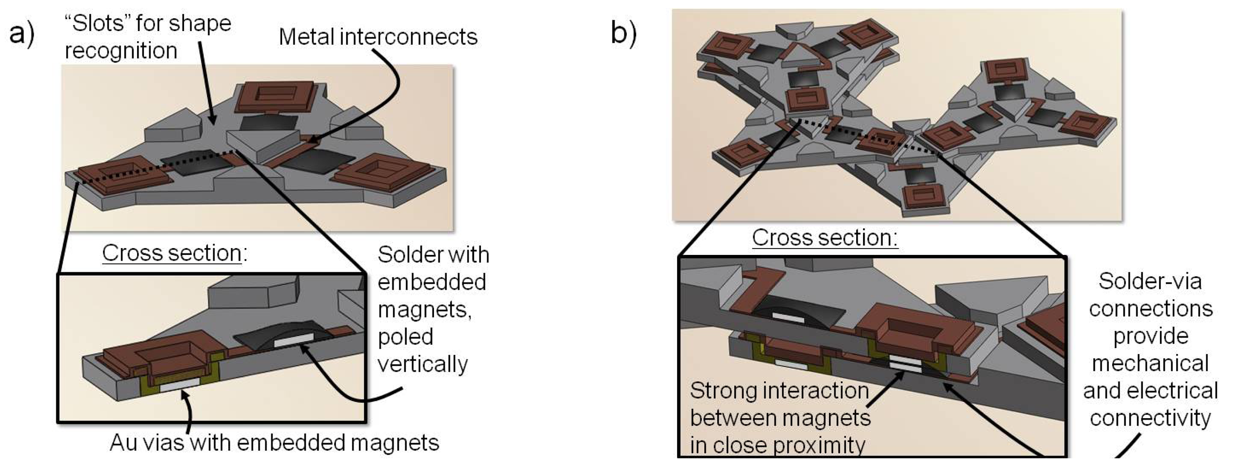
In this paper, we present methods to employ both short-range capillary forces, and the longer range attraction of magnetic forces, to realize a three-dimensional fabrication method which may be used for assembly of future micromachines, electronic circuits, or even three-dimensional meta materials. Our approach is depicted in Figure 1. Figure 1(a) shows a triangular part containing several features designed to insure assembly with other parts to form a three dimensional, electrically-connected network. A slotted geometry and solder alloy deposited on the interior region of the slot allow complimentary shapes to insure correct orientation upon assembly. The geometry of the slot and location of the solder alloy ideally prevent any overlap of the alloy on one part with the alloy on another part encountered in an “upside down” orientation. Electrical vias near the exterior of the slot provide alloy-wetable binding sites on the underside, so that upon assembly in the correct orientation, the alloy and binding site overlap and a capillary bond forms. The interconnect metal, which connects vias, alloy bumps and any embedded circuitry is not wetable by the alloy, to prevent incorrect alloy binding. Furthermore, embedded permanent magnets at the underside of the via surface and at the top of the solder-covered surface help direct proper assembly. Figure 1(b) shows 3-D self-assembled structures, and a cross sectional detail of the 3-D electrical interconnects.
The components depicted in Figure 1 represent a model system to investigate self-assembly as a way to form many layers of circuitry in a parallel fashion, following earlier studies employing molten-alloy based self-assembly with larger, millimeter scale polyurethane parts [35], or hand-fabricated PDMS parts with glued-on electronic components [36]. The following sections describe methods and results for model predictions of magnetic interactions between the structures depicted in Figure 1. We also describe experimental methods to fabricate the parts in Figure 1, using a single crystal silicon substrate and steps, which are entirely compatible as a post process to any CMOS or wafer-scale packaged microelectromechanical device. Finally, we present self-assembly results which build on those presented in a recent conference paper [37].
2. Magnetic Field Calculations
2.1. Methods
Invoking electrostatic analogies, the force on a magnetic dipole characterized by a strength m is determined by the gradient of the magnetic flux density vector field B,
It is advantageous to non-dimensionalize a finite element problem in order to avoid numerical errors associated with extremely large or small numbers, as well as to generalize results to a variety of dimensional cases. Recognizing that the constant of proportionality in Equation (3) must be dimensionless, we defined a non-dimensional force F̄, such that
Here, w is a characteristic length used to non-dimensionalize all length scales, and Br is a material magnetic remanence, used to non-dimensionalize all magnetic flux density values. By selecting μ0 as a characteristic permeability, the permeability of any other material is simply its relative permeability, which is also dimensionless.
We modeled the problem as two rectangular, permanently magnetic blocks using ANSYS (v 12.1, Ansys, Inc., Canonsburg, PA, USA). Each block was characterized by a unit square in the x-y plane and a thickness in the z-direction of 0.16. These dimensionless values corresponded to a 4 μm thick, 25 μm square structure, with the longer dimension defining the characteristic length w for the problem. The blocks were poled along the z-axis. Magnetic properties came from a recently developed CoNiMnP electroplating process resulting in a magnetic remanence Br of 0.22 T, a coercivity Hc of 93 kA/m, and an approximately linear B-H curve between the two values corresponding to a relative permeability of 1.88 [38]. The two blocks contained 11,782 nodes, and an additional 44,513 nodes represented the surrounding air or fluid with a relative permeability of 1. A reduced scalar magnetic potential solver was used to calculate the magnetic flux density vector field, and the force on one block by the other was calculated using the principle of virtual work.
2.2. Results
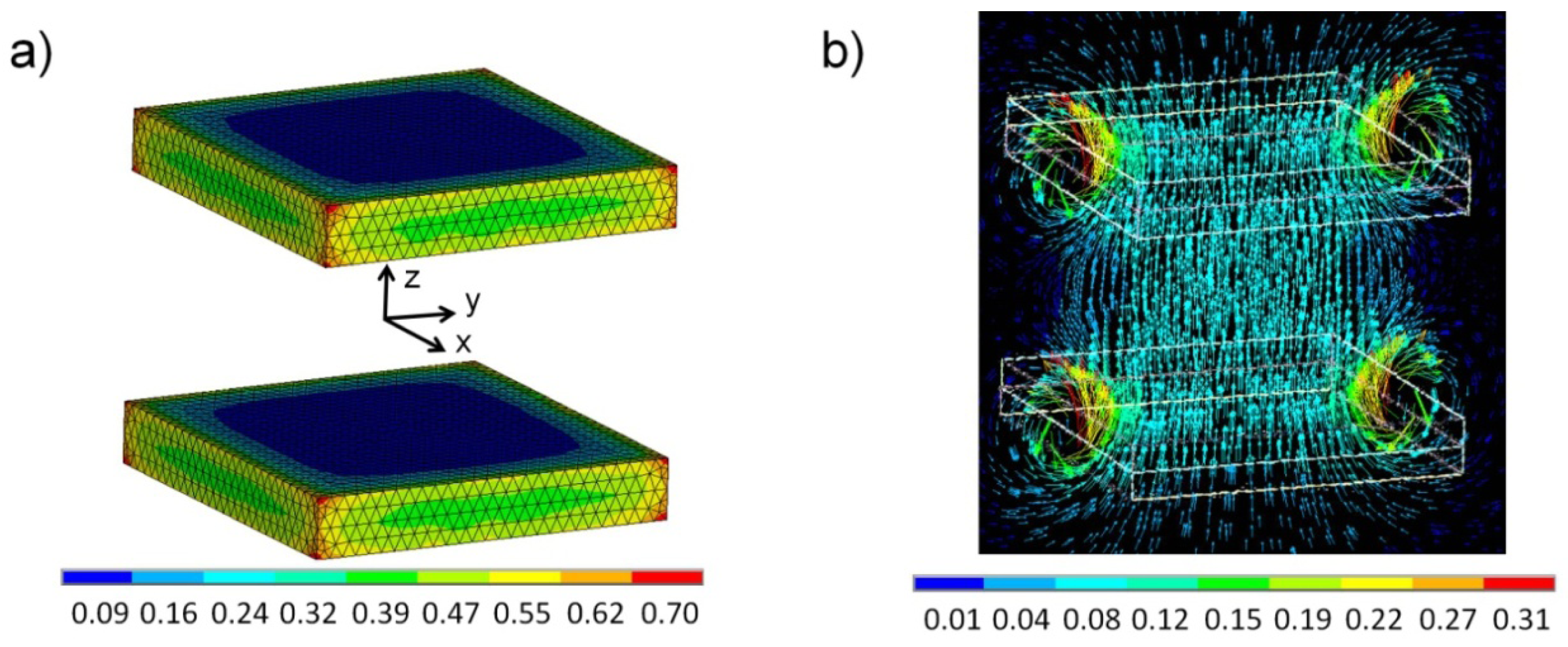
Figure 2 shows representative finite element results for a specific spacing between the blocks of 0.6, corresponding to 15 μm for 25 μm square blocks. Figure 2(a) is a plot of magnetic flux density magnitude contours on the surface of each block, showing that despite the non-dimensional remanence value of unity, the B-field magnitude near the center of each block was only about 0.09. These results illustrate the self-demagnetization effect of low aspect ratio, planar magnetic structures, when those structures are poled in a direction perpendicular to their plane. Figure 2(b) shows the flux density vector plot on the y-z plane at x = 0.
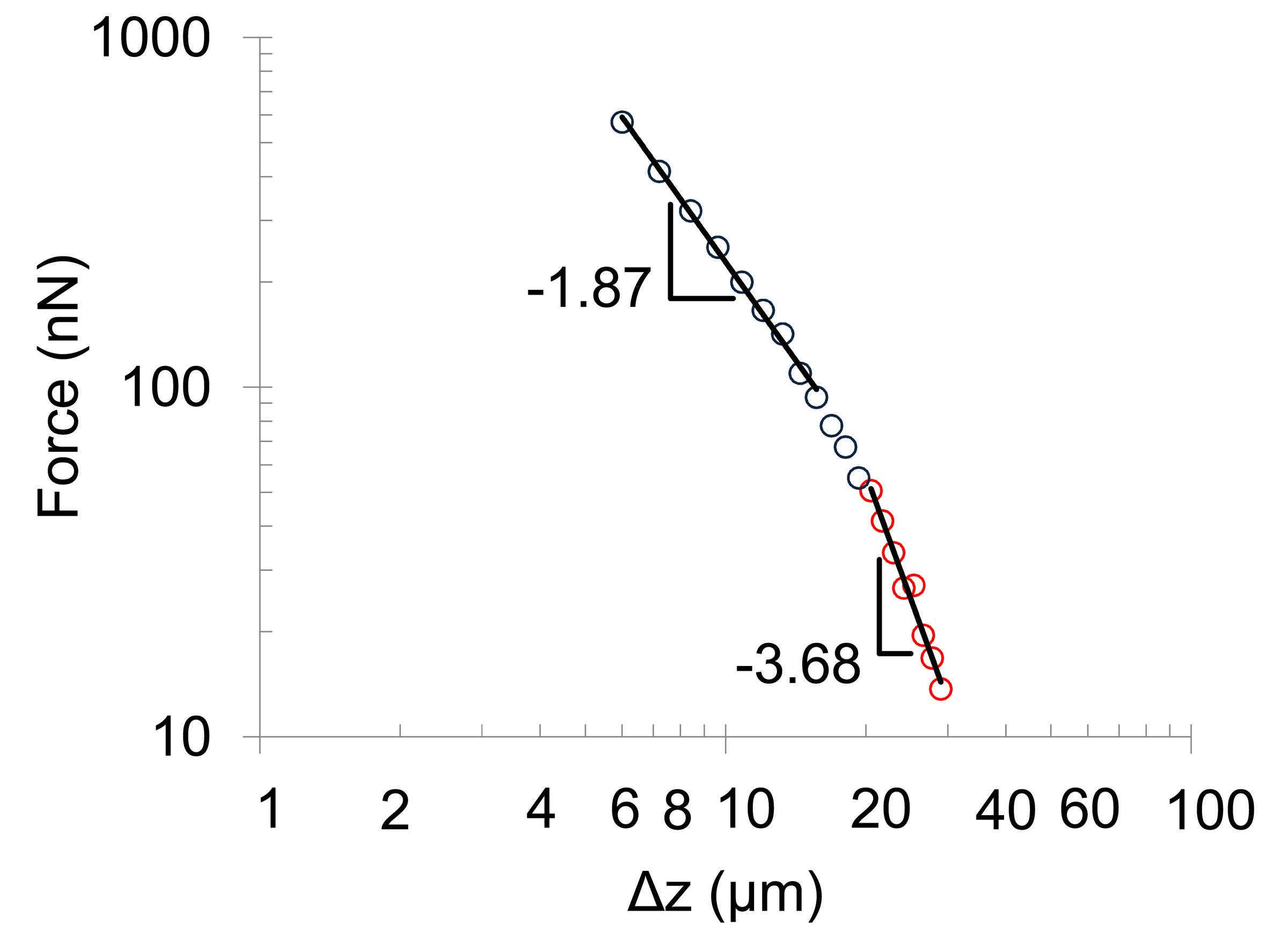
Figure 3 plots the force as a function of distance between the centers of 25 μm square, 4 μm thick magnets, with material properties from [38]. At a distance of 6 μm, a force of over 0.5 μN was present. As indicated by the logarithmic slope values shown in the figure, this force decreased initially according to a 1/r1.87 power law, which approached the expected 1/r2 force law for two magnetic poles. At larger separation distances, the force followed a 1/r3.68 power law, which approached the 1/r4 force law expected for larger separation distances.
Although non-dimensional forces were in the 10−2 to 10−5 range, the actual values were consistent with other microscale forces expected to be present in the experiment described in the following sections. For example, at a distance of 8.3 μm, the magnetic force was equivalent to capillary forces arising from liquid solder, assuming a surface tension of 200 μN/mm acting around the perimeter of a 40 μm square. The magnetic force at this separation distance was also equivalent to low Reynolds number fluidic drag on a 250 μm diameter, 20 μm thick disk by water moving at 135 mm/s [39]. Assuming a density equivalent to that of silicon, this force was also 100 times greater than the gravitational force on the same disk. Therefore, we expected forces from the magnetic blocks to play a significant role in the self-assembly experiment described in the following section.
3. Experimental Methods
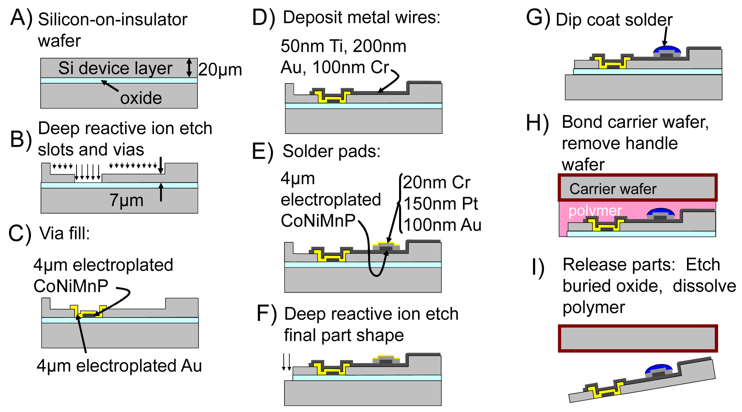
Figure 4 depicts the fabrication process to realize the fully-released, silicon parts containing permanent magnets and the liquid solder regions depicted in Figure 1. First, we started with a silicon-on-insulator (SOI) wafer having a 20 μm device layer as shown in Figure 4(A). We defined slotted features with an intended 13 μm deep reactive ion etch (DRIE), and 40 μm wide vias with another 7 μm DRIE step down to the buried oxide as shown in Figure 4(B). Figure 4(C) shows the partial filling of the vias, first with a 4 μm thick electroplated CoNiMnP alloy, and then with a 4 μm layer of electroplated Au. The magnetic material was electroplated at 10 mA/cm2 from a bath based on findings in [38], with 0.50 mol/L CoSO4·5H2O, 0.5 mol/L NiSO4·6H2O, 0.15 mol/L MnSO4·H2O, 0.65 mol/L H3BO3, 0.40 mol/L NaCl, and 0.05 mol/L of NaH2PO2·H2O. The Au was electroplated in a commercially-available bath (Technigold 25, Technic, Inc., Pawtucket, RI, USA) at 49°C, 3 mA/cm2, and a 1:10 duty cycle (1 ms on, 10 ms off). After photoresist removal, a Au etch solution (GE-8110, Transene, Danvers, MA, USA) removed the seed layer. Next, the metal layers shown in Figure 4(D) included a sputtered interconnect multilayer of 50 nm Ti, 200 nm Au, and 100 nm Cr, patterned by lift-off in acetone. This step was followed by the patterning and electroplating of another set of CoNiMnP magnetic features in Figure 4(E). An evaporated multilayer consisting of 20 nm Cr, 150 nm Pt, and 100 nm Au covered these magnets, and was also patterned by lift-off in acetone. The final part outline was defined by a silicon DRIE step and an oxide RIE etch step depicted in Figure 4(F), resulting in the triangular shapes measuring approximately 280 μm on a side.
We deposited a eutectic Bi-Sn-Pb-In-Cd solder alloy (Indalloy 117, Indium Corporation, Utica, NY, USA) as shown in Figure 4(G). First, a sputtered 50 nm of Au followed by 50 nm of Cu insured that the alloy would wet the entire substrate. We then dipped the wafer through a 160 °C ethylene glycol/solder interface, and the Au and Cu quickly dissolved allowing the alloy to react with the remaining patterned Pt layer. Upon removal of the substrate through this same interface, the alloy dewetted from other areas leaving the alloy only at the prescribed locations. The thickness of the alloy bumps averaged 11.2 μm at their centers, each of which included the 4 μm thick electroplated magnet embedded in the alloy.
The final steps are shown in Figure 4(H), where a carrier wafer was bonded to the device layer using a spin-on polymer (ProTEK A2, Brewer Sciences, Inc., Rolla, MO, USA) and a wafer bonding tool at 1 Torr, 150 °C, and at 1 atm applied pressure. We then removed all but approximately 30 μm of the handle layer by lapping, while a XeF2 etch removed the remaining silicon. Before releasing the parts, the wafer was placed in an 800 kA/m magnetic field to pole the magnets perpendicularly to the wafer plane. Finally, we etched the exposed buried oxide in 49% hydrofluoric acid, and dissolved the ProTEK polymer layer in a dodecene-based solvent (ProTEK Remover 200, Brewer Sciences). The parts quickly sank to the bottom of the solvent container, allowing us to dilute the solvent with IPA by a factor of 103, and follow it by a dilution with DI water by another factor of 103.
For self-assembly, we suspended approximately 103 parts in 3 ml ethylene glycol. The ethylene glycol was previously heated to 85 °C, and contained 10 mM HCl to insure that the solder remained free of surface oxides and able to properly wet intended binding sites. We placed the vial in a heated bath at 85 °C, and began applying fluidic flow pulses of approximately 1 ml discharged through a Pasteur pipette every 1 s to stir the parts. We continued this agitation for 2 min. Whenever a part contacted a liquefied solder binding site, guided by the local magnetic force field immediately beneath that solder site, capillary forces from the solder held the part in place. We then allowed the vial to cool to room temperature which solidified any solder bonds, and diluted the ethylene glycol with ethanol. Finally, we deposited a portion of the solution on a glass slide, and allowed the ethanol to evaporate.
4. Self-Assembly Results and Discussion
Figure 5 shows parts following most fabrication steps but prior to the final solder deposition and final release steps, highlighting both the microscale CoNiMnP magnetic structures, and the successful coating of these structures with solder.
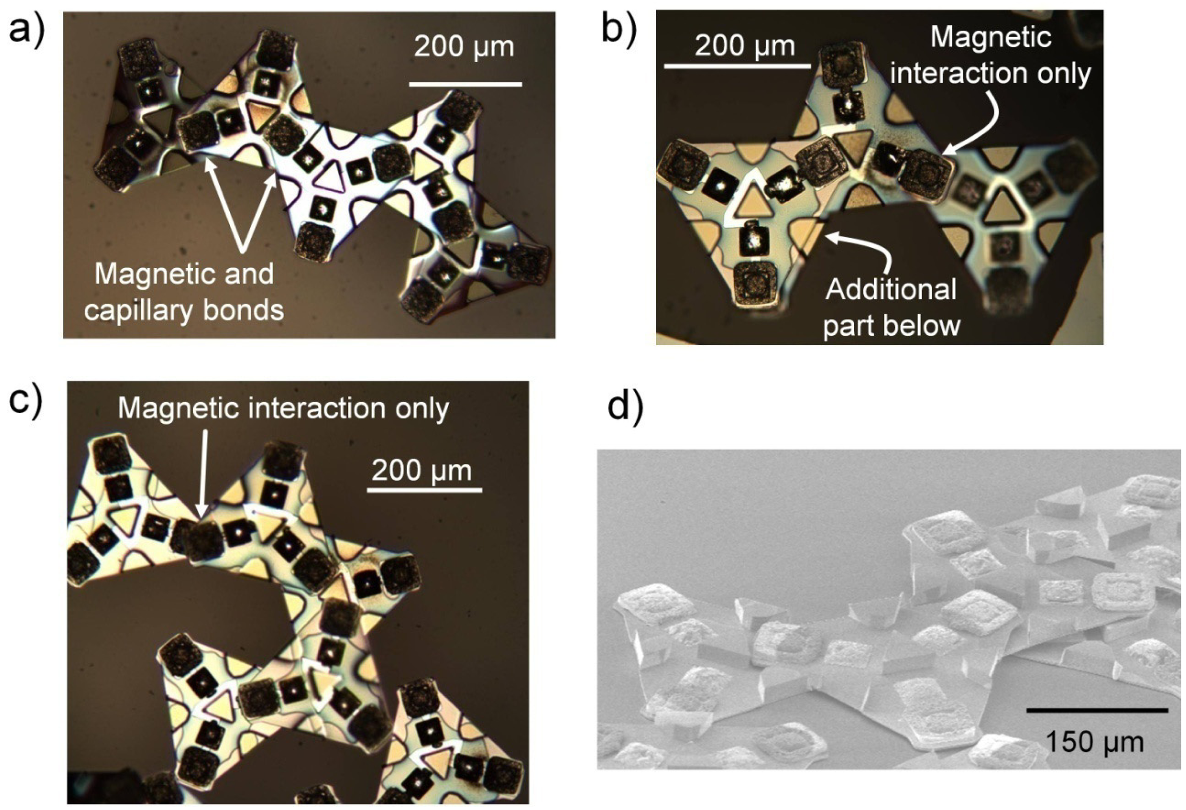
Following the release of these parts, Figure 6 shows several examples of successful self-assembly, in addition to many smaller groups of parts which also assembled correctly but which are not shown. In order to quantify the success of self-assembly, we defined self-assembly yield as the ratio of correct binding events to the total number of possible binding sites with each part. Each part had three binding sites on the front side, and three on the back, for a total of six. Therefore two parts attached correctly with one bond between them counted as two correct binding events—one for each part—out of 12 available binding sites for the two parts. Using this methodology on 362 analyzed parts, we computed an overall yield of 174/2172 = 8.01%.
Although a yield of 8% seems low in comparison to other microscale fluidic self-assembly studies, many of these studies are for less complex structures. For example, Jacobs et al. [7-11,14] all report yields greater than 95% for microscale parts self-assembling on binding sites composed of the same solder alloy used in this study. Similarly high yields are reported for self-assembly on binding sites composed of hydrophobic liquids [5,6]. In each of these cases, parts are pre-concentrated at locally planar binding site surfaces through the use of global forces from gravity, centrifugal rotation, the interfacial energy of immiscible liquids, or some combination of the three. This pre-concentration presents a large number of parts to a smaller number of available binding sites, significantly increasing the rate of correct assembly events in the stochastic self-assembly process. The use of global forces directed toward a binding site plane also helps to insure that liquids wet their intended binding sites and form capillary bonds. That is, with each intended binding site, the forces help to momentarily break the continuous interface of a surface tension bound liquid and form a new interface with the binding site. However, if parts are to self-assemble with one another in more complex 3D structures, as in the present study, localized rather than global force interactions are needed to drive this assembly.
A collection of demonstrations which is particularly relevant to this type of more complex assembly is that of Jacobs et al. [22,23,40,41]. In these studies, approximately 350 μm square, 80 μm thick light emitting diodes (LEDs) self-assemble with larger 800 μm square, 500 μm thick Pyrex carriers, driven by fluidic shear forces to squeeze parts and carriers together in a parallel manner. Yields approach 100% when the ratio of carriers to parts is on the order of 20. However, the assembly of one carrier with one part out of 20 is also equivalent to a binding event yield of 9.5%, using the definition outlined here. When the number of parts equals the number of carriers, [40] shows the overall yield and the binding event yield to be approximately 10%.
Although these studies show that equivalent or even slightly higher yields are possible through the use of capillary forces alone, a source of local energy minimization is still needed prior to the formation of each capillary bond. In the LED/carrier studies, a likely key feature helping the assembly process is the use of tapered sidewalls on each carrier. When a part and a carrier are forced toward one another by fluidic action, physical contact with the tapered sidewalls results in lateral forces which guide the part to its final binding site. In the present experiment, magnetic forces serve the same purpose. Without these localized forces, ultimate yields depend entirely on the low stochastic probability that parts will come into contact with each other in exactly the right orientation. Considering our previous work with similar parts intended to self-assemble into the same complex 3D structures, the binding event yield drops to about 0.1% when no localized forces are used [42]. But with localized forces, our study together with former studies show that yields increase to 8–10%.
Magnetic forces should ultimately achieve much higher yields with careful control over design tolerances. In the present study, unintended magnetic interactions led to unintended binding orientations. The parts were actually etched to a much greater depth than expected during the first etch step (17.4 μm instead of 13 μm), resulting in a very thin base layer evident in the images of Figure 5 and in Figure 6(d). This thin layer caused magnets located at the back side of each outer via to lie at nearly the same plane as the magnets embedded in each inner, front side solder bump. This proximity caused magnetic interactions between outer vias of two parts to be of the same magnitude as those intended between inner solder bumps and outer vias. Therefore, the back side outer via on one part could magnetically bind with the front side outer via of another part, preventing the stronger capillary and solder bonds from ever forming. In Figure 6(b,c), a total of four otherwise correct binding events seem to have been prevented by this type of unintended magnetic interaction. Although only observed 0.6% of the time upon inspection following assembly, cooling, and drying, this type of unintended binding probably occurred much more often during the actual assembly process, because weak magnetic bonds could be easily broken by subsequent handling processes. According to calculations in Section 2, we expect that even a few micrometers of additional separation between the planes of inner and outer magnets, achieved through better control over fabrication tolerances, will greatly reduce the incidence of this assembly defect and increase overall yield.
Another incorrect orientation observed less frequently was the stacking of one part on top of another. The stacking of two parts on the left side of Figure 6(b) was actually correct, but in some cases parts stacked without the intended intermediate part. This stacking was also caused by magnetic interaction between pairs of inner and outer magnets, and again we postulate it likely occurred much more frequently during actual assembly. An alternative fabrication process utilizing thicker photoresist and non-contact lithography would enable the patterning of recessed features and vias at depths of 30–50 μm. This process would allow greater separation between unintended magnetic interactions, significantly reducing their strength, and lead to much higher yields.
At some point, even perfectly designed and fabricated parts would be difficult to self-assemble with 100% yield, because as the rate of correct assembly events increases, so will the likelihood of voids appearing in the growing crystalline structure. It is conceivable to alternatively create the same structure using a patterned template to order the first layer of parts, then to expose a new set of binding sites on these assembled parts, and to continue the layer-by-layer process until the desired structure thickness is achieved. This method would require the development of selective binding techniques to limit each step to the assembly of a single layer of parts, which other than initial demonstrations of electrochemically controlled hydrophobicity [5] or solders with different melting points [8], remains an area for future research. Regardless of the self-assembly methods pursued, as the complexity and three dimensionality of desired structures increase, we expect localized forces from magnetic fields to help achieve far greater yields than without the use of these forces.
4. Conclusions
In summary, we have demonstrated magnetic forces combined with capillary forces to provide a route towards three dimensional, interconnected self-assembly. A finite element model of magnetic forces between permanent magnet blocks demonstrated the utility of magnetic forces at micrometer scales. We have detailed the fabrication of fully-released microfabricated parts designed to assemble in a particular fashion, including the incorporation of both permanent magnet structures and a low melting point solder alloy. A yield of 8% resulted, which was a significant improvement over past yields of less than 0.1% when capillary forces were used alone. We expect additional improvements with further refinements to the fabrication process, enabling the self-assembly of future micromachines, three-dimensional electronic circuit architectures, or meta-material crystal structures.

References
- Mastrangeli, M.; Abbasi, S.; Varel, C.; Hoof, C.V.; Celis, J.P.; Böhringer, K.F. Self-assembly from milli- to nanoscales: methods and applications. J. Micromech. Microeng. 2009, 19, 083001. [Google Scholar]
- Morris, C.J.; Stauth, S.A.; Parviz, B.A. Self-assembly for micro and nano scale packaging: Steps toward self-packaging. IEEE Trans. Adv. Packag. 2005, 28, 600–611. [Google Scholar]
- Srinivasan, U.; Helmbrecht, M.; Rembe, C.; Muller, R.; Howe, R. Fluidic self-assembly of micromirrors onto microactuators using capillary forces. IEEE J. Sel. Topics Quantum Electr. 2002, 8, 4–11. [Google Scholar]
- Srinivasan, U.; Liepmann, D.; Howe, R.T. Microstructure to substrate self-assembly using capillary forces. J. Microelectromechan. Syst. 2001, 10, 17–24. [Google Scholar]
- Xiong, X.; Hanein, Y.; Fang, J.; Wang, Y.; Wang, W.; Schwartz, D.T.; Böhringer, K.F. Controlled multibatch self-assembly of microdevices. J. Microelectromechanical Syst. 2003, 12, 117–127. [Google Scholar]
- Scott, K.L.; Hirano, T.; Yang, H.; Singh, H.; Howe, R.T.; Niknejad, A.M. High-performance inductors using capillary based fluidic self-assembly. J. Microelectromechanical Syst. 2004, 13, 300–309. [Google Scholar]
- Jacobs, H.O.; Tao, A.R.; Schwartz, A.; Gracias, D.H.; Whitesides, G.M. Fabrication of a cylindrical display by patterned assembly. Science 2002, 296, 323–325. [Google Scholar]
- Liu, M.; Lau, W.M.; Yang, J. On-demand multi-batch self-assembly of hybrid mems by patterning solders of different melting points. J. Micromech. Microeng. 2007, 17, 2163–2168. [Google Scholar]
- Stauth, S.A.; Parviz, B.A. Self-assembled single-crystal silicon circuits on plastic. Proc. Natl. Acad. Sci. U.S.A. 2006, 103, 13922–13927. [Google Scholar]
- Chung, J.; Zheng, W.; Hatch, T.J.; Jacobs, H.O. Programmable reconfigurable self-assembly: Parallel heterogeneous integration of chip-scale components on planar and nonplanar surfaces. J. Microelectromechanical Syst. 2006, 15, 457–464. [Google Scholar]
- Morris, C.J.; Parviz, B.A. Micro-scale metal contacts for capillary force-driven self-assembly. J. Micromech. Microeng. 2008, 18, 015022. [Google Scholar]
- Morris, C.J.; Dubey, M. Micro-scale self-assembly using molten alloys with different melting points. J. Vac. Sci. Technol. B 2008, 26, 2534–2538. [Google Scholar]
- Arscott, S.; Peytavit, E.; Vu, D.; Rowe, A.C.H.; Paget, D. Fluidic assembly of hybrid MEMS: a GaAs-based microcantilever spin injector. J. Micromech. Microeng. 2010, 20, 025023. [Google Scholar]
- Knuesel, R.J.; Jacobs, H.O. Self-assembly of microscopic chiplets at a liquid-liquid-solid interface forming a flexible segmented monocrystalline solar cell. Proc. Natl. Acad. Sci. USA 2010, 107, 993–998. [Google Scholar]
- Chen, C.H.; Yu, T.H.; Lee, Y.C. Direct patterning of metallic micro/nano-structures on flexible polymer substrates by roller-based contact printing and infrared heating. J. Micromech. Microeng. 2010, 20, 025034. [Google Scholar]
- Kim, D.; Ahn, J.; Choi, W.M.; Kim, H.; Kim, T.; Song, J.; Huang, Y.Y.; Liu, Z.; Lu, C.; Rogers, J.A. Stretchable and foldable silicon integrated circuits. Science 2008, 320, 507–511. [Google Scholar]
- Onoe, H.; Iwase, E.; Matsumoto, K.; Shimoyama, I. Three-dimensional integration of heterogeneous silicon micro-structures by liftoff and stamping transfer. J. Micromech. Microeng. 2007, 17, 1818–1827. [Google Scholar]
- Park, S.; Xiong, Y.; Kim, R.; Elvikis, P.; Meitl, M.; Kim, D.; Wu, J.; Yoon, J.; Yu, C.; Liu, Z.; Huang, Y.; chih Hwang, K.; Ferreira, P.; Li, X.; Choquette, K.; Rogers, J.A. Printed assemblies of inorganic Light-Emitting diodes for deformable and semitransparent displays. Science 2009, 325, 977–981. [Google Scholar]
- Clark, T.D.; Ferrigno, R.; Tien, J.; Paul, K.E.; Whitesides, G.M. Template-directed self-assembly of 10-μm-sized hexagonal plates. J. Am. Chem. Soc. 2002, 124, 5419–5426. [Google Scholar]
- Clark, T.D.; Tien, J.; Duffy, D.C.; Paul, K.E.; Whitesides, G.M. Self-assembly of 10-μm-sized objects into ordered three-dimensional arrays. J. Am. Chem. Soc. 2001, 123, 7677–7682. [Google Scholar]
- Morris, C.J.; Ho, H.; Parviz, B.A. Liquid polymer deposition on free-standing microfabricated parts for self-assembly. J. Microelectromechanical Syst. 2006, 15, 1795. [Google Scholar]
- Zheng, W.; Buhlmann, P.; Jacobs, H.O. Sequential shape-and-solder-directed self-assembly of functional microsystems. Proc. Natl. Acad. Sci. USA 2004, 101, 12814–12817. [Google Scholar]
- Zheng, W.; Jacobs, H.O. Shape-and-solder-directed self-assembly to package semiconductor device segments. Appl. Phys. Lett. 2004, 85, 3635–3637. [Google Scholar]
- Fonstad, C.G., Jr.; Zahn, M. Method and system for magnetically assisted statistical assembly of wafers 2005. United States Patent 6,888,178, 3 May 2005. [Google Scholar]
- Ramadan, Q.; Uk, Y.S.; Vaidyanathan, K. Large scale microcomponents assembly using an external magnetic array. Appl. Phys. Lett. 2007, 90, 172502–3. [Google Scholar]
- Rivero, R.; Shet, S.; Booty, M.; Fiory, A.; Ravindra, N. Modeling of magnetic-field-assisted assembly of semiconductor devices. J. Electr. Mater. 2008, 37, 374–378. [Google Scholar]
- Shetye, S.; Eskinazi, I.; Arnold, D. Magnetic self-assembly of millimeter-scale components with angular orientation. J. Microelectromechanical Syst. 2010, 19, 599–609. [Google Scholar]
- Grzybowski, B.A.; Stone, H.A.; Whitesides, G.M. Dynamics of self assembly of magnetized disks rotating at the liquid-air interface. Proc. Natl. Acad. Sci. USA 2002, 99, 4147–51. [Google Scholar]
- Iwase, E.; Shimoyama, I. Multi-step sequential batch self-assembly of three-dimensional micro-structures using magnetic field. Proceedings of 18th IEEE International Conference on MEMS 2005, Miami, FL, USA, January 30–February 3, 2005; pp. 588–591.
- Wang, D.A.; Ko, H.H. Magnetic-assisted self-assembly of rectangular-shaped parts. Sens. Actuat. A: Phys. 2009, 151, 195–202. [Google Scholar]
- Shetye, S.B.; Eskinazi, I.; Arnold, D.P. Self-assembly of millimeter-scale components using integrated micromagnets. IEEE Trans. Magn. 2008, 44, 4293–4296. [Google Scholar]
- Love, J.C.; Urbach, A.R.; Prentiss, M.G.; Whitesides, G.M. Three-dimensional self-assembly of metallic rods with submicron diameters using magnetic interactions. J. Am. Chem. Soc. 2003, 125, 12696–12697. [Google Scholar]
- Tanase, M.; Silevitch, D.M.; Hultgren, A.; Bauer, L.A.; Searson, P.C.; Meyer, G.J.; Reich, D.H. Magnetic trapping and self-assembly of multicomponent nanowires. J. Appl. Phys. 2002, 91, 8549–8551. [Google Scholar]
- Ye, H.; Gu, Z.; Yu, T.; Gracias, D.H. Integrating nanowires with substrates using directed assembly and nanoscale soldering. IEEE Trans. Nanotechnol. 2006, 5, 62–66. [Google Scholar]
- Terfort, A.; Whitesides, G.M. Self-assembly of an operating electrical circuit based on shape complementarity and the hydrophobic effect. Adv. Mater. 1998, 10, 470–473. [Google Scholar]
- Gracias, D.H.; Tien, J.; Breen, T.L.; Hsu, C.; Whitesides, G.M. Forming electrical networks in three dimensions by Self-Assembly. Science 2000, 289, 1170–1172. [Google Scholar]
- Morris, C.J.; Laflin, K.E.; Isaacson, B.; Grapes, M.; Gracias, D.H. Capillary and magnetic forces for microscale self-assembled systems. Proceeding of Integrated Miniaturized Materials-From Self-Assembly to Device Integration, of Materials Research Symposium, San Francisco, CA, USA, April 5ȓ9, 2010; 1272.
- Grapes, M.D.; Morris, C.J. Optimizing the CoNiMnP electrodeposition process using Taguchi design of experiments. J. Electrochem. Soc. 2010, 157, D642–D647. [Google Scholar]
- White, F.M. Viscous Fluid Flow, 2nd ed.; McGraw Hill: Columbus, OH, USA, 1991. [Google Scholar]
- Zheng, W.; Jacobs, H. Fabrication of multicomponent microsystems by directed three-dimensional self-assembly. Adv. Funct. Mater. 2005, 15, 732–738. [Google Scholar]
- Zheng, W.; Jaehoon, C.; Jacobs, H.O. Fluidic heterogeneous microsystems assembly and packaging. J. Microelectromechanical Syst. 2006, 15, 864–870. [Google Scholar]
- Morris, C.J.; Dubey, M. Toward three dimensional circuits formed by molten-alloy driven self-assembly. Proceedings of 26th Annual Army Science Conference, Orlando, FL, USA, December 1–4, 2008.
© 2011 by the authors; licensee MDPI, Basel, Switzerland. This article is an open access article distributed under the terms and conditions of the Creative Commons Attribution license (http://creativecommons.org/licenses/by/3.0/).
Share and Cite
Morris, C.J.; Isaacson, B.; Grapes, M.D.; Dubey, M. Self-Assembly of Microscale Parts through Magnetic and Capillary Interactions. Micromachines 2011, 2, 69-81. https://doi.org/10.3390/mi2010069
Morris CJ, Isaacson B, Grapes MD, Dubey M. Self-Assembly of Microscale Parts through Magnetic and Capillary Interactions. Micromachines. 2011; 2(1):69-81. https://doi.org/10.3390/mi2010069
Chicago/Turabian StyleMorris, Christopher J., Brian Isaacson, Michael D. Grapes, and Madan Dubey. 2011. "Self-Assembly of Microscale Parts through Magnetic and Capillary Interactions" Micromachines 2, no. 1: 69-81. https://doi.org/10.3390/mi2010069
APA StyleMorris, C. J., Isaacson, B., Grapes, M. D., & Dubey, M. (2011). Self-Assembly of Microscale Parts through Magnetic and Capillary Interactions. Micromachines, 2(1), 69-81. https://doi.org/10.3390/mi2010069


