1. Introduction
Tandem solar cells represent an important route toward surpassing the efficiency limit of single-junction photovoltaics through integrating wide-bandgap and narrow-bandgap subcells with a complementary absorption range [
1,
2,
3]. Among the various tandem configurations, perovskite/silicon tandem solar cells are developing particularly rapidly because they combine the tunable bandgap and strong optical absorption of perovskites with the technological maturity of crystalline silicon [
4,
5]. Considering spectral utilization and current matching in series-connected devices, the optimal bandgap of the perovskite top-cell absorber is generally considered to be approximately 1.68–1.72 eV [
6,
7,
8]. At present, high-performance wide-bandgap top cells are mainly based on organic–inorganic hybrid I/Br mixed-halide perovskites with high Br contents [
9,
10]. In recent years, the power conversion efficiency of 1.68 eV wide-bandgap single-junction perovskite solar cells has reached values beyond 24%, contributing to certified efficiencies above 34% for perovskite/silicon tandem devices [
11]. However, increasing the Br content tends to aggravate the initial inhomogeneous distribution of halides and light-induced halide migration in I/Br mixed-halide perovskites, leading to the formation of I-rich and Br-rich phases, local bandgap narrowing, enhanced nonradiative recombination, and open-circuit voltage losses [
12,
13,
14]. In addition, the organic A-site cations in hybrid perovskites are susceptible to volatilization or decomposition under prolonged heating and illumination, which further limits the long-term operational stability of wide-bandgap top cells [
15,
16,
17].
All-inorganic CsPbI
3 has an optical bandgap of approximately 1.70–1.73 eV, which closely matches the bandgap required for the top cell in perovskite/silicon tandem solar cells [
18,
19,
20]. Unlike high-Br I/Br mixed-halide perovskites, CsPbI
3 contains only iodide as the halide component and therefore intrinsically avoids light-induced Br/I phase segregation. Meanwhile, replacing volatile organic A-site cations with inorganic Cs
+ is beneficial for improving the intrinsic photothermal stability of the material [
21,
22,
23]. CsPbI
3 is therefore regarded as a highly promising wide-bandgap absorber for tandem solar cells [
24]. Nevertheless, owing to its relatively small Goldschmidt tolerance factor, photoactive black-phase CsPbI
3 remains thermodynamically prone to transforming into the non-photoactive yellow δ phase at room temperature [
25,
26]. Although compositional regulation, additive engineering, energy-level optimization, and interfacial passivation have increased the power conversion efficiency of CsPbI
3 solar cells to above 22% in recent years [
27], their overall performance still lags behind that of advanced hybrid wide-bandgap perovskite devices, indicating that crystallization defects and carrier recombination losses in CsPbI
3 films have not yet been fully resolved.
The formation of CsPbI
3 films generally involves precursor coordination, intermediate-phase formation, and thermally induced transformation into the black phase [
28,
29]. During solvent evaporation and thermal annealing, rapid and spatially nonuniform nucleation and crystal growth can readily produce small grains, dense grain boundaries, local pinholes, and disordered crystal orientations [
30,
31]. Meanwhile, incomplete lattice formation and local nonstoichiometry can generate iodine vacancies, Pb-related defects, and undercoordinated ions, which introduce carrier trap states within the bandgap [
32]. These defects not only aggravate nonradiative recombination in the bulk and at grain boundaries, resulting in losses in open-circuit voltage and fill factor, but may also provide pathways for moisture penetration and ion migration, thereby accelerating black-phase degradation and device performance decay [
33,
34]. Therefore, the formation of compact and uniform CsPbI
3 films with large grains and low trap-state densities is essential for further improving device efficiency and operational stability.
Introducing dimethylammonium iodide (DMAI) into CsPbI
3 precursor solutions is one of the most widely used approaches for regulating crystallization [
35,
36]. It is reported that DMAI can participate in the formation of DMA
+-containing intermediate phases and alter the nucleation, crystal growth, and phase-transition pathways of CsPbI
3, thereby lowering the formation temperature of black-phase CsPbI
3 and improving film coverage. Early studies generally regarded DMAI as a volatile additive that could be removed during high-temperature annealing. However, subsequently it was revealed that DMAI-derived films may initially form mixed compositions such as Cs
1−xDMA
xPbI
3, and that their final compositions are highly dependent on the annealing temperature, annealing duration, film thickness, and ambient conditions. Residual DMA
+ and related intermediate phases that are not fully removed can alter the local lattice structure, chemical composition, and bandgap of CsPbI
3 and may compromise device thermal stability. On the other hand, the controlled retention of DMA-containing species has also been used to construct CsPbI
3/Cs
1−xDMA
xPbI
3 bulk heterojunctions, yielding a device efficiency of 20.32%. These findings indicate that DMA-containing species cannot simply be regarded as completely volatile additives because their crystallization-regulating effects are closely coupled with their final residual states. Therefore, controlling the amount and chemical form of residual DMA
+ while retaining its beneficial role in intermediate-phase regulation remains an important issue in DMAI-assisted CsPbI
3 fabrication.
To further improve the crystallization quality of CsPbI
3 films, various additive strategies have been developed to regulate precursor coordination, intermediate-phase formation, and phase-transition kinetics. Yu et al. developed a urea–ammonium thiocyanate molten salt, in which the coordination interaction between SCN
− and Pb
2+ regulated the precursor chemical environment and promoted the formation of high-quality CsPbI
3 films, resulting in a device efficiency above 20% and a stabilized output efficiency of 19.2% [
37]. Duan et al. introduced formamidine acetate into the precursor and altered the phase-transition pathway of CsPbI
3 by inducing an additional intermediate phase, thereby obtaining phase-pure γ-CsPbI
3 films with high crystallinity and device efficiencies above 18% [
38]. Cui et al. further employed the room-temperature molten salt dimethylamine acetate (DMAAc) as both a precursor solvent and a phase-transition regulator, enabling effective control over CsPbI
3 crystallization and yielding an open-circuit voltage of 1.25 V and power conversion efficiencies above 21% [
39]. Wang et al. introduced the acyloin ligand 1,2-di(thiophen-2-yl)ethane-1,2-dione, whose interaction with undercoordinated Pb
2+ stabilized the γ phase and passivated defects, resulting in a device efficiency of 21.15% [
22]. More recently, Li et al. used sulfonic zwitterions to regulate the nucleation and crystal growth of inverted CsPbI
3 films, suppressing defect-mediated recombination and further increasing the device efficiency to above 22% [
40].
These studies demonstrate that salts or organic molecules with specific coordination capabilities can effectively improve CsPbI3 film quality and device performance by regulating intermediate-phase evolution. However, existing additives often contain bulky organic components, which may passivate defects and stabilize the lattice when remaining at grain boundaries or grain surfaces, whereas excessive residues may alter the local chemical composition, dielectric environment, and grain-boundary barriers, or even form low-dimensional phases or carrier-transport-blocking layers. Therefore, it is more important to develop additive systems with simple compositions, well-defined crystallization-regulation mechanisms, and controllable residual behavior. Dimethylammonium (DMA) salts represent such a class of additives. Their simple ionic structures allow the roles of the DMA+ cation and the counteranion in precursor coordination, intermediate-phase formation, and crystal growth to be systematically investigated. The previously reported DMA-salt-assisted strategies have mainly focused on DMAI and DMAAc. DMAI provides both DMA+ and I− and primarily regulates black-phase formation through the formation of DMA-containing iodoplumbate intermediate phases. In contrast, DMAAc relies on the coordination between acetate and Pb2+ and can also act as a room-temperature molten-salt solvent to modify the precursor chemical environment. Therefore, the coordination between anion and Pb2+ also plays an important role during crystallization process. Compared with these additives, DMACl retains the intermediate-phase-regulating capability of DMA+ while introducing Cl− with distinctly different chemical properties, which may further alter the Pb-halide coordination environment, intermediate-phase conversion, and crystal-growth kinetics. Therefore, investigating the effects of DMACl on the nucleation, crystal growth, defect formation, and energy-level structure of CsPbI3 can not only clarify the roles of different anions in DMA-salt-assisted crystallization but may also provide a simpler strategy for preparing high-quality CsPbI3 films.
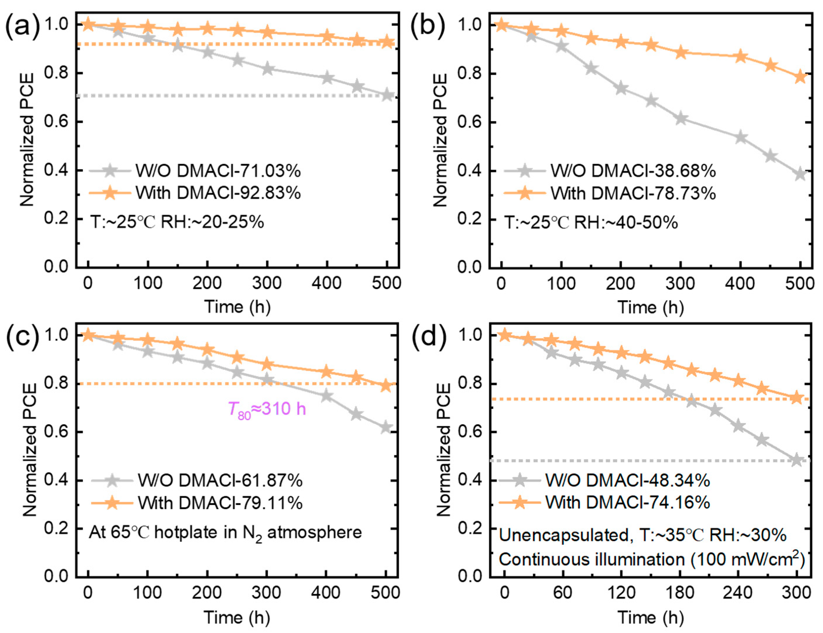
In this work, dimethylammonium chloride (DMACl) was employed to regulate the crystallization of CsPbI3 films. The introduction of DMACl altered the nucleation and crystal-growth behavior of CsPbI3. Concretely, it promoted grain growth and improved film compactness and crystallinity. Meanwhile, DMACl treatment significantly reduced the trap-state density, prolonged the carrier lifetime, and suppressed nonradiative recombination in both the bulk film and at the interfaces. DMACl shifted the conduction-band minimum (CBM) and valence-band maximum (VBM) of CsPbI3 upward, reduced the energy-level offset between the CBM of CsPbI3 and the lowest unoccupied molecular orbital (LUMO) of PC61BM, and thereby facilitated electron extraction. Benefiting from the synergistic improvements in film crystallinity, defect passivation, and interfacial carrier transport, the reverse-scan power conversion efficiency (PCE) increased from 18.99% to 20.97%, while the stabilized output efficiency at the maximum power point reached 20.5%. DMACl treatment also significantly enhanced device stability under humid, thermal-aging, and continuous-illumination conditions. In particular, under thermal aging at 65 °C, the T80 lifetime was extended from approximately 310 h to approximately 485 h. These results demonstrate that changing the anionic component of DMA salts can simultaneously regulate the crystallization kinetics, defect formation, and energy-level alignment of CsPbI3, providing an effective strategy for constructing efficient and stable all-inorganic wide-bandgap perovskite solar cells.
3. Results and Discussion
We first investigated the effects of DMACl on the crystallization and surface properties of CsPbI
3 films. As shown in
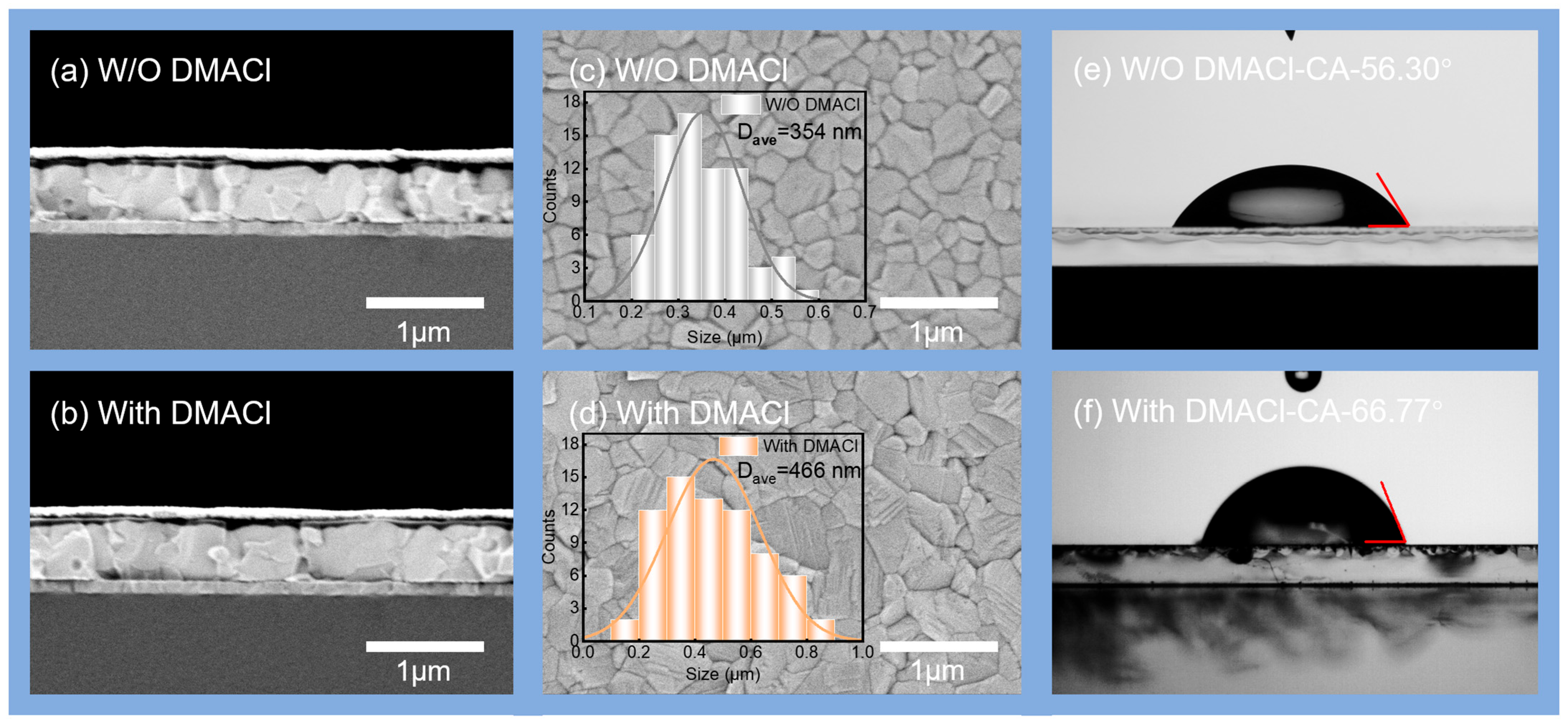
Figure 1a,b, the relatively thick layer in the middle of the device cross-section corresponds to the CsPbI
3 perovskite absorber layer. Continuous perovskite layers were formed in both devices; however, compared with the control device without DMACl, the DMACl-treated perovskite layer exhibited a denser morphology and markedly larger grains in the cross-section. Such large grains along the vertical direction can reduce the number of grain boundaries encountered during carrier transport, thereby suppressing grain-boundary-related recombination losses. The top-view SEM images further confirmed the promoting effect of DMACl on the grain growth of CsPbI
3 (
Figure 1c,d). The film without DMACl consisted of relatively small grains with an average grain size of approximately 354 nm; after the introduction of DMACl, the grain size increased markedly to approximately 466 nm, accompanied by a corresponding decrease in the number of grain boundaries. The cross-sectional and top-view SEM results collectively demonstrate that DMACl regulates the nucleation and crystal-growth processes of CsPbI
3, promotes grain growth, and improves film compactness. The XRD results further revealed the effect of DMACl on the crystallization properties of the films (
Figure S1). Both films exhibited the characteristic diffraction peaks of black-phase CsPbI
3, with the main peaks assigned to the (110) and (220) planes, and no obvious additional diffraction peaks appeared after DMACl treatment, indicating that the introduction of DMACl did not alter the dominant crystal phase of CsPbI
3. Compared with the control film, the DMACl-treated film exhibited significantly enhanced characteristic diffraction peaks, indicating improved crystallinity. This result is consistent with the enlarged grains and increased film compactness observed by SEM.
In addition to the crystallization morphology, DMACl also markedly altered the surface wettability of the CsPbI
3 films. As shown in
Figure 1e,f, the water contact angle increased from 52.30° for the CsPbI
3 film without DMACl to 68.77° after DMACl treatment, indicating enhanced surface hydrophobicity. This change may, on the one hand, be associated with the DMACl-induced grain growth and changes in the film surface morphology; on the other hand, it may also be related to the retention or enrichment of DMA
+ and trace DMA–haloplumbate complexes at the film surface or grain boundaries. DMACl participates in intermediate-phase formation during crystallization, and as the CsPbI
3 lattice continues to grow and become more ordered, the relatively bulky DMA
+ cations are unlikely to be stably incorporated into the final CsPbI
3 lattice and may therefore be gradually expelled toward the grain surfaces or grain-boundary regions, thereby altering the surface chemical composition and surface energy of the film.
To further examine this possibility, KPFM measurements were performed, and the results showed that the surface potential of the CsPbI
3 film also changed markedly after DMACl treatment (
Figure S2). KPFM measurement was performed in the sample-biased configuration, where the bias voltage was applied to the sample while the tip was electrically grounded. Line-scan profiles extracted over the same distance showed that the surface potential increased from approximately 60 mV for the control film to approximately 130 mV after DMACl treatment (
Figure S3). Meanwhile, the DMACl-treated film exhibited a more uniform potential distribution, indicating a more homogeneous surface electronic environment and reduced local energy-level fluctuations. Combined with the change in water contact angle, these results suggest that, after regulating crystal growth, some DMA-related species may become enriched at the film surface or grain boundaries and interact with undercoordinated ions or defect sites, thereby modifying the surface potential and wettability. For an inverted configuration, this elevated top-surface potential enlarges the electrostatic potential gradient across the absorber, thereby strengthening the built-in field to facilitate electron extraction toward the top PC
61BM layer while suppressing interfacial charge accumulation.
We first investigated the photoluminescence properties of the films and the electrical characteristics of the devices to verify whether DMACl can reduce defects in CsPbI
3 films and suppress nonradiative recombination. As shown in
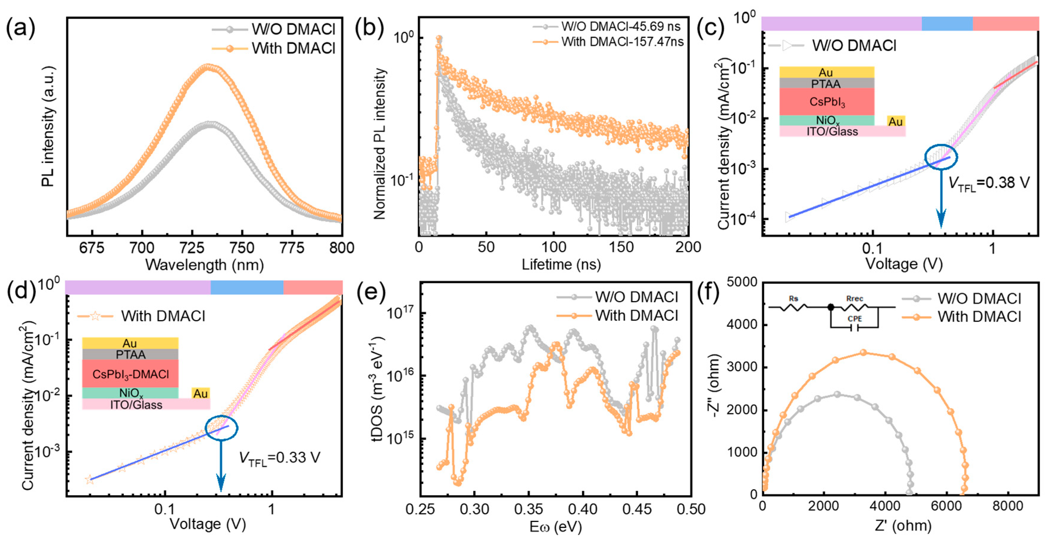
Figure 2a, the DMACl-treated film exhibits a significantly enhanced steady-state photoluminescence intensity compared with the control film without DMACl. Under identical measurement conditions, stronger photoluminescence from the perovskite film generally indicates that defect-induced nonradiative recombination is suppressed. Time-resolved photoluminescence measurements further confirm this result. The emission peak centers at 733 nm, which is in close agreement with the absorption cutoff (734 nm) and the optical bandgap of 1.69 eV determined from the Tauc plots (
Figure S4). The negligible Stokes shift and preserved emission position indicate that DMACl does not alter the fundamental bandgap. The subtle sub-bandgap optical feature observed in the DMACl-treated film arises from diffuse light scattering induced by the noticeably enlarged crystal grains rather than deep defect states. As shown in
Figure 2b, the average carrier lifetime increases from 45.69 ns for the control film to 157.47 ns after DMACl treatment. The substantially prolonged carrier lifetime indicates that DMACl reduces the probability of carrier trapping and nonradiative energy loss, thereby improving the optoelectronic quality of the CsPbI
3 films.
The defect states in the films were further investigated using space-charge-limited current measurements. As shown in
Figure 2c,d, hole-only devices with a structure of ITO/NiO
x/CsPbI
3/PTAA/Au were fabricated. According to the dark current–voltage curves, the trap-filled limit voltage decreases from 0.38 V for the device without DMACl to 0.33 V for the DMACl-treated device. The trap-state defect density
can be obtained from the following equation:
where
,
(
= 6.5),
and
L represent the permittivity of free space, relative permittivity, elementary charge, and film thickness, respectively. The calculated trap densities are 1.09 × 10
15 cm
−3 and 0.95 × 10
15 cm
−3. When the film thickness and relative dielectric constant remain essentially unchanged, a lower trap-filled limit voltage corresponds to a lower trap-state density, indicating that DMACl effectively reduces the carrier traps in the CsPbI
3 films. This result is consistent with the conclusions obtained from the steady-state and time-resolved photoluminescence measurements.
To further examine the variation in defect states at different energy levels, we analyzed the trap density-of-states distribution of the devices. As shown in
Figure 2e, the DMACl-treated sample exhibits a lower trap density of states over most of the measured energy range than the control sample, indicating that DMACl not only reduces the overall defect density but also suppresses the formation of trap states at different depths. Combined with the previously observed grain enlargement and reduction in grain-boundary density, the decreased trap density may arise from both the improved crystallization quality of the films and the interactions between DMA-related species and undercoordinated ions.
Electrochemical impedance spectroscopy further reveals the effect of DMACl on carrier recombination within the devices. As shown in
Figure 2f, the Nyquist plot of the DMACl-treated device exhibits a larger semicircle diameter. According to the equivalent-circuit fitting, the semicircle diameter is mainly associated with the recombination resistance of the device; therefore, the larger semicircle indicates a higher recombination resistance and weaker interfacial carrier recombination in the DMACl-treated device. These results demonstrate that the reduction in defects induced by DMACl further improves the carrier-transport and recombination dynamics within the device.
We next evaluated the effects of DMACl on the surface chemical environment and electronic structure of CsPbI
3. As shown in
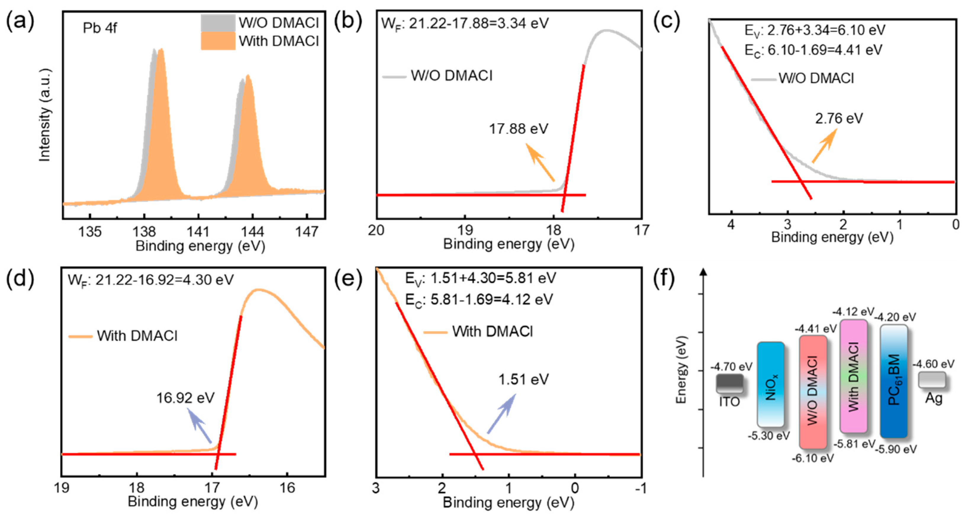
Figure 3a, the XPS spectra of both films exhibit the characteristic Pb 4f doublet, corresponding to Pb 4f
7/2 and Pb 4f
5/2, respectively. After DMACl treatment, the Pb 4f peaks shift by 0.4 eV toward higher binding energy, indicating that DMACl alters the local chemical environment of surface Pb ions. Combined with the aforementioned contact-angle, KPFM, and defect-related measurements, this change in the Pb chemical environment may arise from the interaction between DMA-related species distributed at the perovskite surface and undercoordinated Pb sites, thereby contributing to surface defect regulation.
Ultraviolet photoelectron spectroscopy (UPS) was subsequently employed to further investigate the effect of DMACl on the energy-level structure of CsPbI
3. As shown in
Figure 3b,d, based on the secondary electron cutoff and the equation W
F = hν − E
cutoff, the work functions of the CsPbI
3 films without and with DMACl treatment were calculated to be 3.34 and 4.30 eV, respectively, indicating that the introduction of DMACl significantly shifts the Fermi-level position of the CsPbI
3 film. Meanwhile, the valence-band onset also changes markedly. As shown in
Figure 3c,e, the valence-band onset of the control film is located approximately 2.76 eV below the Fermi level, whereas this value decreases to approximately 1.51 eV after DMACl treatment. Accordingly, the valence-band maxima of the control and DMACl-treated CsPbI
3 films were calculated to be approximately −6.10 and −5.81 eV, respectively. Combined with the optical bandgap of approximately 1.69 eV for CsPbI
3 (
Figure S4), the corresponding conduction-band minima were further determined. The conduction-band minimum of CsPbI
3 is approximately −4.41 eV without DMACl and shifts upward to approximately −4.12 eV after DMACl treatment. Based on these energy-level values, the corresponding device energy-level diagram was constructed, as shown in
Figure 3f. For the CsPbI
3 film without DMACl, the conduction-band minimum is located at −4.41 eV, resulting in an energy offset of approximately 0.21 eV relative to the LUMO level of PC
61BM (approximately −4.20 eV), which is unfavorable for electron transfer from the perovskite to the electron transport layer. After DMACl treatment, the conduction-band minimum of CsPbI
3 shifts upward to −4.12 eV, leading to improved energy-level matching with the LUMO of PC
61BM and changing the interfacial electron-transfer process from an energetically unfavorable alignment to an almost barrier-free or slightly downhill pathway. Therefore, the DMACl-induced energy-level reconstruction facilitates electron extraction at the CsPbI
3/PC
61BM interface and reduces interfacial carrier accumulation and recombination losses.
Taken together, the XPS and UPS results, along with the above analyses, indicate that DMACl not only reduces defects in CsPbI3 films by regulating the crystallization process, but may also leave DMACl-derived species at the film surface or grain boundaries after crystallization, where they could simultaneously contribute to defect passivation and surface energy-level regulation, thereby providing a more favorable interfacial environment for efficient carrier extraction and transport.
To evaluate the effect of DMACl treatment on the photovoltaic performance of CsPbI
3 solar cells, inverted PSCs with a device architecture of Glass/ITO/NiO
x/CsPbI
3/PC
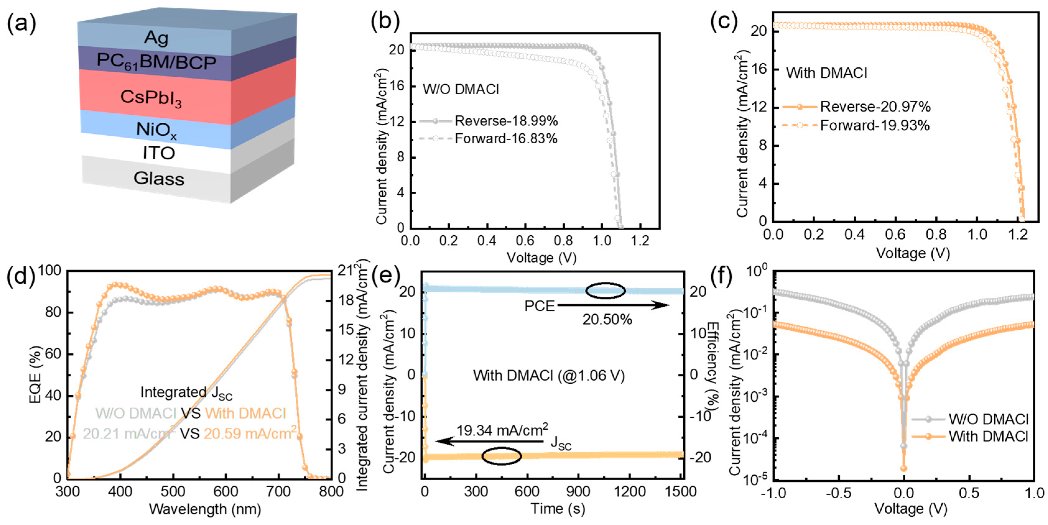
61BM/BCP/Ag were fabricated, as schematically illustrated in
Figure 4a. The concentration of DMACl was first optimized from 0 to 1.50 mg mL
−1, and the corresponding photovoltaic parameters are summarized in
Figure S5 and Table S1. The device performance initially increased with increasing DMACl concentration and reached the optimum at 1.00 mg mL
−1. A further increase in DMACl concentration to 1.50 mg mL
−1 resulted in a slight decrease in device efficiency.
Figure 4b,c show the J-V characteristics of the champion devices without and with DMACl treatment, respectively. The control device exhibited a reverse-scan PCE of 18.99%, whereas the DMACl-treated device achieved a substantially improved PCE of 20.97% with the corresponding, V
OC, J
SC and FF of 1.230 V, 20.70 mA cm
−2, and 82.37%, respectively. Notably, the performance enhancement induced by DMACl was predominantly associated with the pronounced increase in V
OC. In addition, the DMACl-treated device exhibited suppressed photovoltaic hysteresis. To further verify the reproducibility of the performance improvement, 18 independent devices were fabricated for each condition, and their photovoltaic parameters were statistically analyzed (
Figure S6). Compared with the control devices, the DMACl-treated devices exhibited a clear upward shift in the PCE distribution, accompanied by a pronounced increase in V
OC. The distributions of J
SC and FF also showed moderate improvements. The external quantum efficiency (EQE) spectra are presented in
Figure 4d. Both devices exhibited broad photo-responses over the wavelength range of approximately 300–750 nm. The integrated values derived from the EQE spectra were 20.21 and 20.59 mA cm
−2 for the control and DMACl-treated devices, respectively, very close to the values obtained from the J-V measurements. The steady-state power output of the optimized DMACl-treated device was further evaluated at its maximum power point. As shown in
Figure 4e, under a constant bias of 1.06 V, the device maintained a stable current density of approximately 19.34 mA cm
−2 over 1500 s, corresponding to a stabilized PCE of 20.50%. The stabilized efficiency is close to the PCE obtained from the reverse J-V scan, confirming the reliable power output of the device. To gain further insight into the origin of the enhanced V
OC, Mott–Schottky measurements were performed on the control and DMACl-treated devices. As shown in
Figure S7, the built-in potential (V
bi) increased markedly from 0.885 V for the control device to 1.223 V after DMACl treatment. The enhanced V
bi indicates a stronger internal electric field across the device, which is favorable for charge-carrier separation and extraction while suppressing interfacial carrier recombination. This result is consistent with the energy-level alignment analysis and the photovoltaic performance of the solar cells. Furthermore, as shown in
Figure 4f, the DMACl-treated device exhibited a markedly reduced dark current density compared with the control device. The suppressed leakage current suggests reduced nonradiative charge recombination, which is consistent with enhanced photovoltaic performance.
In addition to the improved photovoltaic performance, the influence of DMACl treatment on device stability was systematically evaluated under different aging conditions. As shown in
Figure 5a, after storage for 500 h at approximately 25 °C and a relatively low humidity of 20–25% RH, the control device retained only 71.03% of its initial PCE, whereas the DMACl-treated device maintained 92.83% of its initial efficiency. The performance difference between the control device and the DMACl-treated device became more pronounced after aging under a higher humidity of 40–50% RH (
Figure 5b), where the retained PCE increased from 38.68% for the control device to 78.73% after DMACl treatment, demonstrating substantially improved resistance to moisture-induced degradation. Such improvement in moisture stability can be correlated with the more hydrophobic surface induced by DMACl, which retards the moisture penetration. The thermal stability of the devices at 65 °C under an N
2 atmosphere was further evaluated (
Figure 5c); the control device exhibited continuous performance degradation and reached a T
80 of approximately 310 h, retaining only 61.87% of its initial PCE after 500 h. In contrast, the DMACl-treated device showed a considerably slower degradation and retained 79.11% of its initial efficiency after aging for 500 h. Since moisture was largely excluded under this condition, we assigned the enhanced thermal stability to the less defective perovskite network, which is less susceptible to defect-mediated structural degradation under prolonged thermal stress. More importantly, the DMACl-treated devices also exhibited improved stability under continuous operation. The unencapsulated devices were subjected to continuous illumination at 100 mW cm
−2 under approximately 35 °C and 30% RH to assess the light-soaking stability of DMACl treatment (
Figure 5d). After 300 h of continuous illumination, the control device retained only 48.34% of its initial PCE, whereas the DMACl-treated device maintained 74.16%. Namyoung Ahn et al. demonstrated that the accumulation and trapping of photogenerated carriers at grain boundaries or perovskite/charge-transport-layer interfaces can act synergistically with moisture to accelerate irreversible perovskite degradation, highlighting that device stability depends not only on suppressing moisture ingress but also on minimizing localized charge accumulation (trapped charge-driven degradation of perovskite solar cells). In the present study, the improved stability of the DMACl-treated devices under simultaneous illumination and humid conditions can therefore be associated with several mutually reinforcing effects induced by DMACl treatment, including enhanced surface hydrophobicity, improved interfacial carrier extraction, and reduced defect density. The increased hydrophobicity is expected to retard moisture penetration, whereas more efficient carrier extraction and fewer trap states reduce the propensity for carrier trapping and accumulation at defect-rich regions and interfaces. Together, these effects provide a plausible explanation for the substantially enhanced light–humidity stability of the DMACl-treated devices.