3.1. Theoretical and Experimental Investigation of the Piezoelectric Device
The electric charge generated by a piezoelectric element is directly proportional to the local mechanical strain, which in turn is proportional to the bending moment at the element’s position along the composite plate. Therefore, the electrical contribution of each element depends on its spatial location relative to the region of maximum curvature.
Because the maximum bending strain and curvature occur near the clamped central region of the plate, the piezoelectric elements located closest to the center generate the highest voltages and currents.
As the distance from the center increases, the bending moment and corresponding strain decrease progressively, leading to reduced electrical output from elements positioned toward the plate edges.
Due to the independent rectification stage assigned to each piezoelectric element, capacitive voltage equalization between elements is avoided. Instead, the rectified charges are cumulatively transferred to the storage capacitor. As a result, the output voltage depends on the total accumulated charge, pulse duration, and hand-pulling time, while the output current corresponds to the sum of the individual rectified currents.
For the investigated configurations (1 × 9 and 2 × 9 piezo elements), the experimentally validated proportionality coefficients describing the spatial strain distribution along one half of the plate are described by
and
.
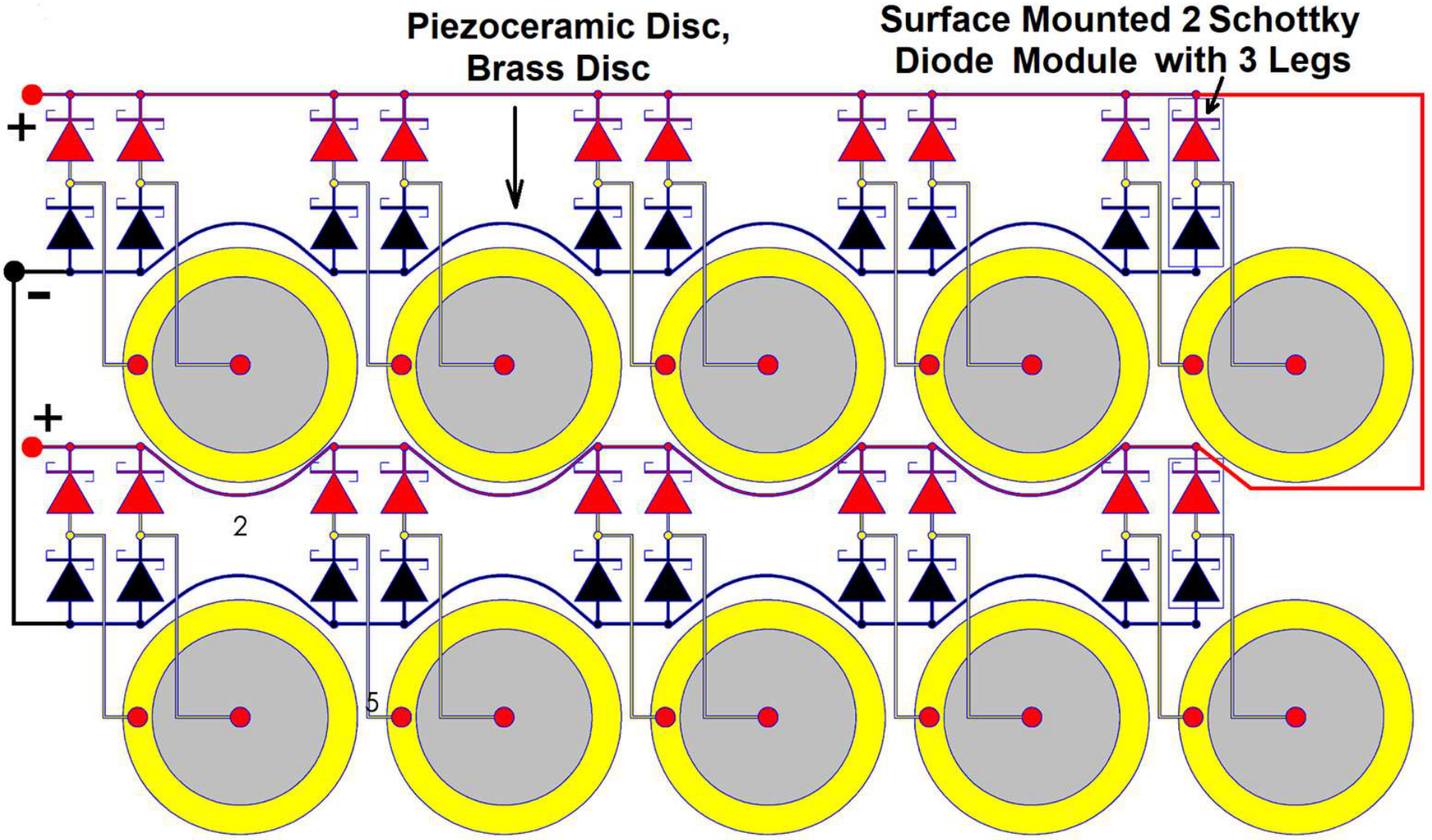
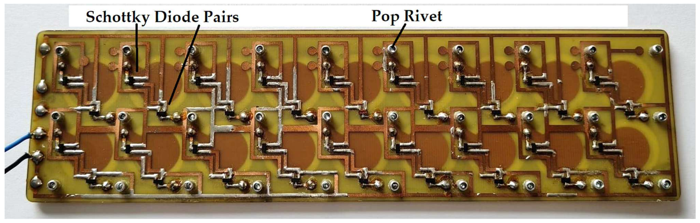
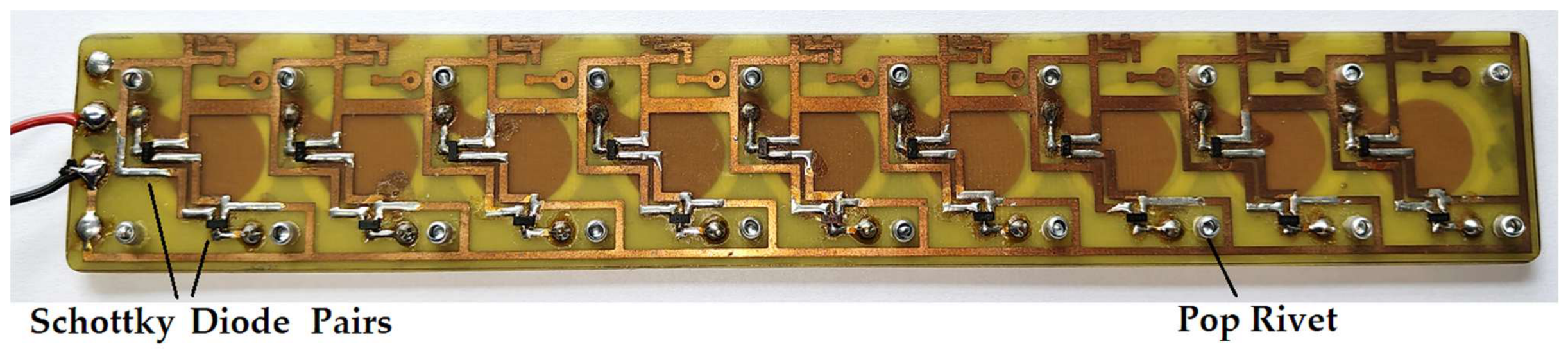
Distance from the composite plate center gradually changes from 22 mm up to 88 mm, with a step size of 22 mm. The distance between pop rivets centers is also 22 mm. Each piezo is surrounded by four pop rivets.
For , and for , . The coefficients were experimentally determined from at least 20 repeated measurements based on the mean voltage and current values obtained at each applied force. These measurements were conducted with only the central SMD Schottky rectifier bridges connected, after which the remaining rectifiers were progressively added to the piezoelectric-element columns, and the measurements were repeated.
Across both plates (nine and 18 piezoelectric elements), the quadratic fitting model showed strong agreement with the experimental data, with coefficients of determination (R2) values ranging from 0.990 to 0.998, correlation coefficients from 0.993 to 0.998, and average relative errors between approximately 2% and 5% for the measured voltage.
These coefficients represent the relative contribution of the piezoelectric elements to the strain distribution along the plate.
For an ideal symmetric bending configuration, the strain distribution is expected to vary approximately quadratically (decrease) with the distance from the clamped center. This ideal case corresponds to giving at positions from the plate center. The experimentally obtained values for are close to this ideal distribution, indicating that the proposed geometry closely matches the mechanical strain profile of the bending plate. Therefore, the geometry can be considered near-optimal for coupling the strain field to the spatial distribution of the piezoelectric elements.
For short, when the plate is clamped at the center and loaded at the edges, the bending moment—and therefore the mechanical strain—is maximum at the center and decreases gradually toward the edges, following an approximately quadratic law. Because the piezoelectric voltage and generated charge are proportional to the local strain, the elements located near the center produce the largest electrical output, while those toward the edges generate progressively smaller voltages and currents.
By spacing the piezoelectric discs uniformly (22 mm center-to-center) along the plate length, the array samples the strain field at regular intervals. This configuration ensures that the central elements operate near their maximum strain while the outer elements still contribute useful electrical charge instead of occupying regions where the deformation would be too small to produce significant output. Furthermore, the symmetric placement of two piezoelectric discs across the plate width at each longitudinal position allows both sides of the plate to experience nearly identical deformation. This symmetry improves the effective current generation because the electrical contributions from elements subjected to similar strain are summed after rectification.
The combination of optimized inter-element spacing, symmetric arrangement, and individual Schottky rectification enables the piezoelectric array to capture a substantial portion of the bending strain energy available in the plate and to function collectively as an equivalent larger piezoelectric disc. Consequently, the system attains a relatively high electrical output (approximately 63 V and 5.2 mW) using only 18 small piezoelectric elements.
This distribution indicates that the entire assembly that contains nine piezoelectric elements behaves electrically as approximately 5.92–6.32 centrally located piezoelectric elements operating under maximum strain conditions. In addition, this distribution shows that the entire assembly incorporating 18 piezoelectric elements behaves electrically as approximately 11.84–12.64 centrally located piezoelectric elements operating under maximum strain conditions (at 47 N). The bending moment and the curvature distribution is not linear, but it fits very well to this quadratic model, from Equation (1).
Mechanically, the system operates in a clean and symmetric manner, featuring a centrally stiffened plate and thin PCB laminates (0.4 mm each), with the neutral axis reinforced by rivets. The rectifier-per-piezo configuration offers several advantages: it enables proper (non-destructive) charge summation, prevents capacitive cancellation, avoids losses due to phase mismatch, and maximizes the harvested energy by capturing additional contributions even from the smallest curvatures present at the plate edges.
In the center of the plate , and four piezoelectric elements are distributed symmetrically along the plate, for 2 × 9 piezoelectric elements. For the plate with nine piezoelectric elements , and , one is distributed symmetrically to the left side, and the other is distributed symmetrically to the right side (from the center). The electromechanical coupling factor was determined experimentally for the plate with nine piezoelectric elements. In addition, for the composite plate containing 18 piezoelectric elements, the electromechanical coupling factor was . Theoretically, this factor depends on the effective stiffness, Young modulus, composite disk geometry (thickness and surface area), and piezoelectric coefficients.
The electromechanical coupling factor for the composite plate containing nine piezoelectric elements was experimentally determined to be approximately . For the composite plate containing 18 piezoelectric elements, the coupling factor increased to approximately . Theoretically, this factor depends on the effective stiffness, Young’s modulus, geometric parameters of the composite disk (including thickness and surface area), and the piezoelectric coefficients of the active material. Although the composite plate containing 18 piezoelectric elements exhibited a larger electromechanical coupling factor, the softer composite plate can generate higher output voltages under mechanical excitation due to its lower effective stiffness. The reduced stiffness allows larger bending deformation and, consequently, higher mechanical strain in the piezoelectric layer under the same applied force. Since the generated electrical charge is directly related to the induced strain, the more compliant structure can produce higher open-circuit voltages despite its lower force factor. In contrast, the stiffer composite plate undergoes smaller deformation under identical loading conditions, resulting in reduced strain-induced voltage generation. All voltage measurements were performed under open-circuit conditions.
Since the electrical capacitance of a single piezoceramic element with a diameter of 15 mm, bonded to a 20 mm brass disk, is , and the maximum hand-motion frequency is approximately 4–5 Hz, the average current generated by one central piezoelectric element after full-bridge rectification was estimated to be . This value is in good agreement with the experimentally measured current obtained under a bending force of 47 N for the composite plate containing 18 piezoelectric elements.
For the same bending force, the voltage generated by the central piezoelectric element mounted in the composite plate containing the 1 × 9 piezoelectric array was , whereas the corresponding voltage measured for the composite plate containing the 2 × 9 piezoelectric array was . The higher voltage generated by the 1 × 9 configuration is attributed to its lower effective stiffness, which allows larger bending deformation and consequently higher strain levels in the piezoelectric material.
As said earlier, the individual (per column) voltage measurements were performed before mounting the remaining SMD Schottky rectifier bridges on the composite plate surface; only the two central rectifier bridges were connected during the initial measurements. Subsequently, the Schottky rectifiers were progressively added for each column containing one or two piezoelectric elements, and the corresponding voltage measurements were repeated. Using these experimental data, the and coefficients were determined for each position on the composite plate.
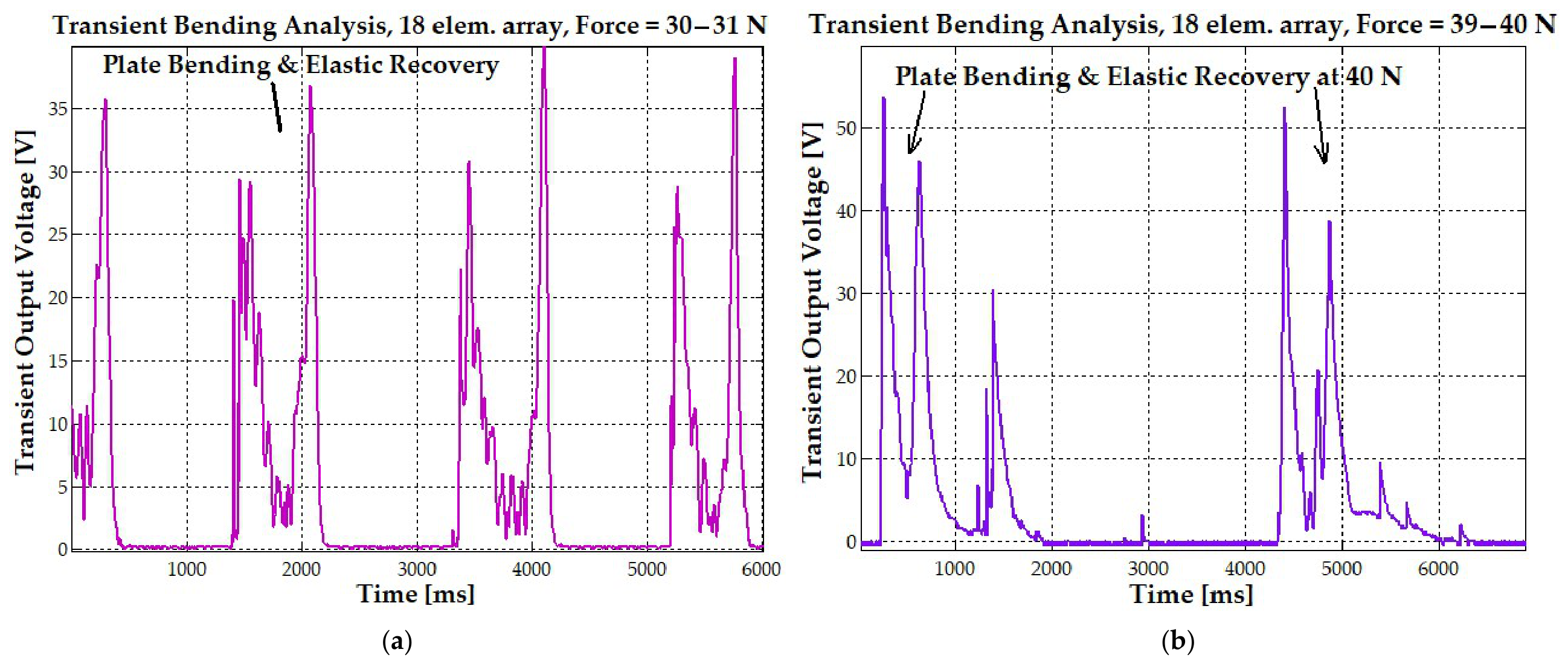
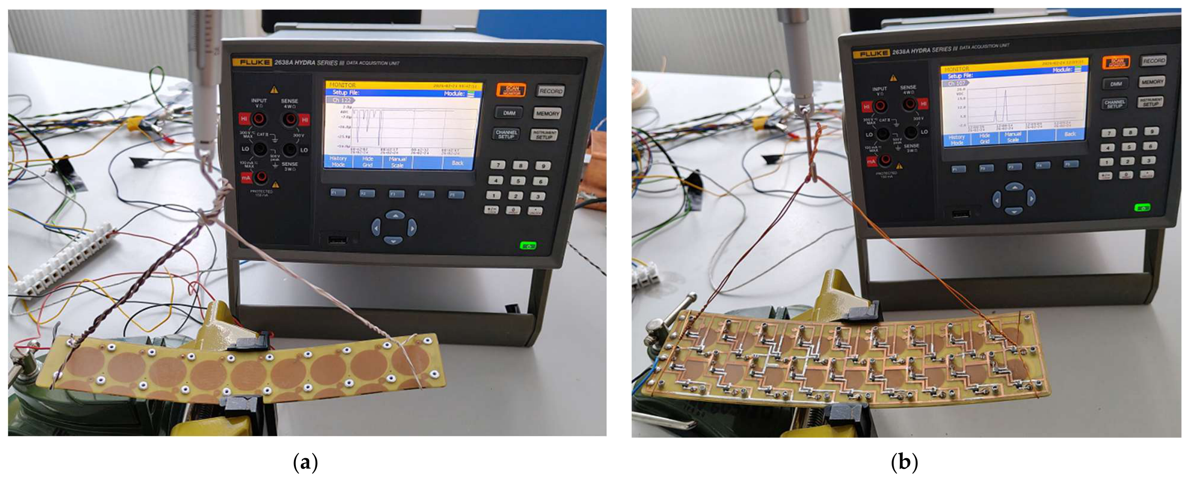
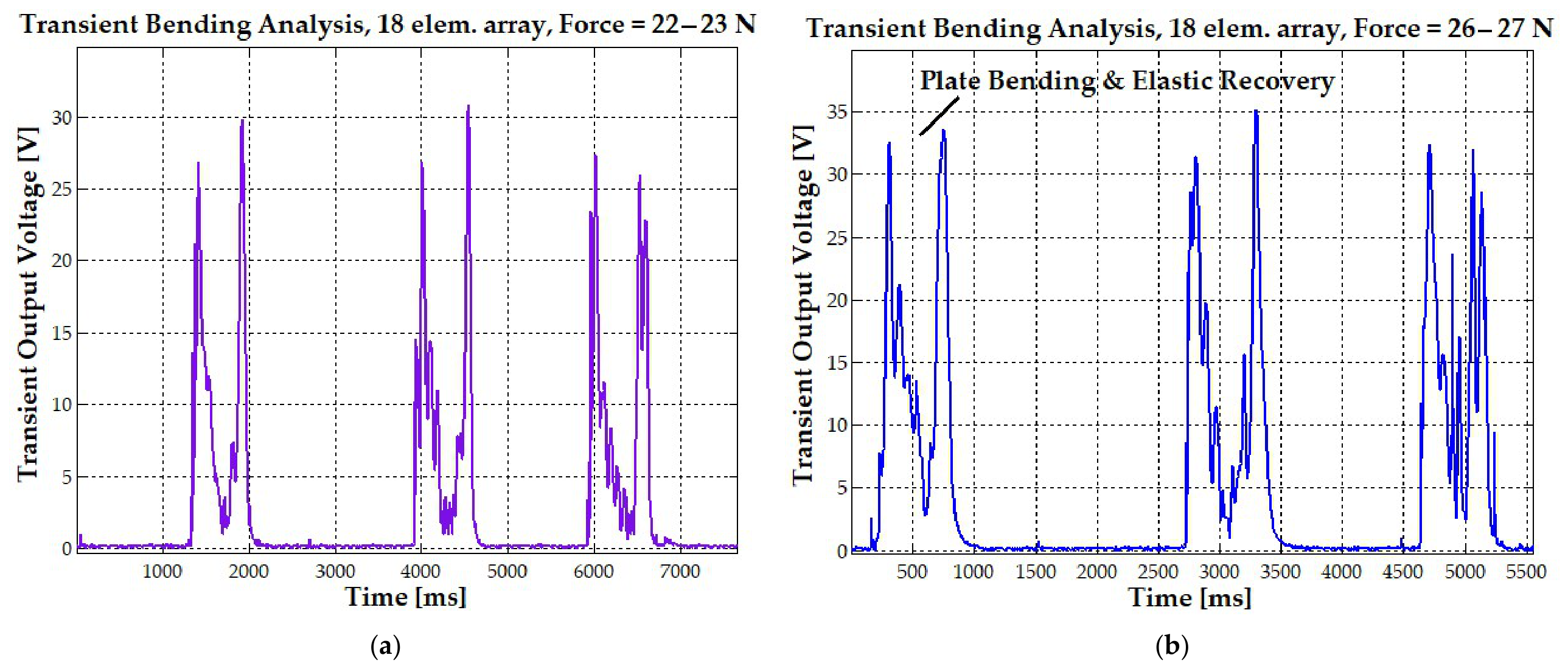
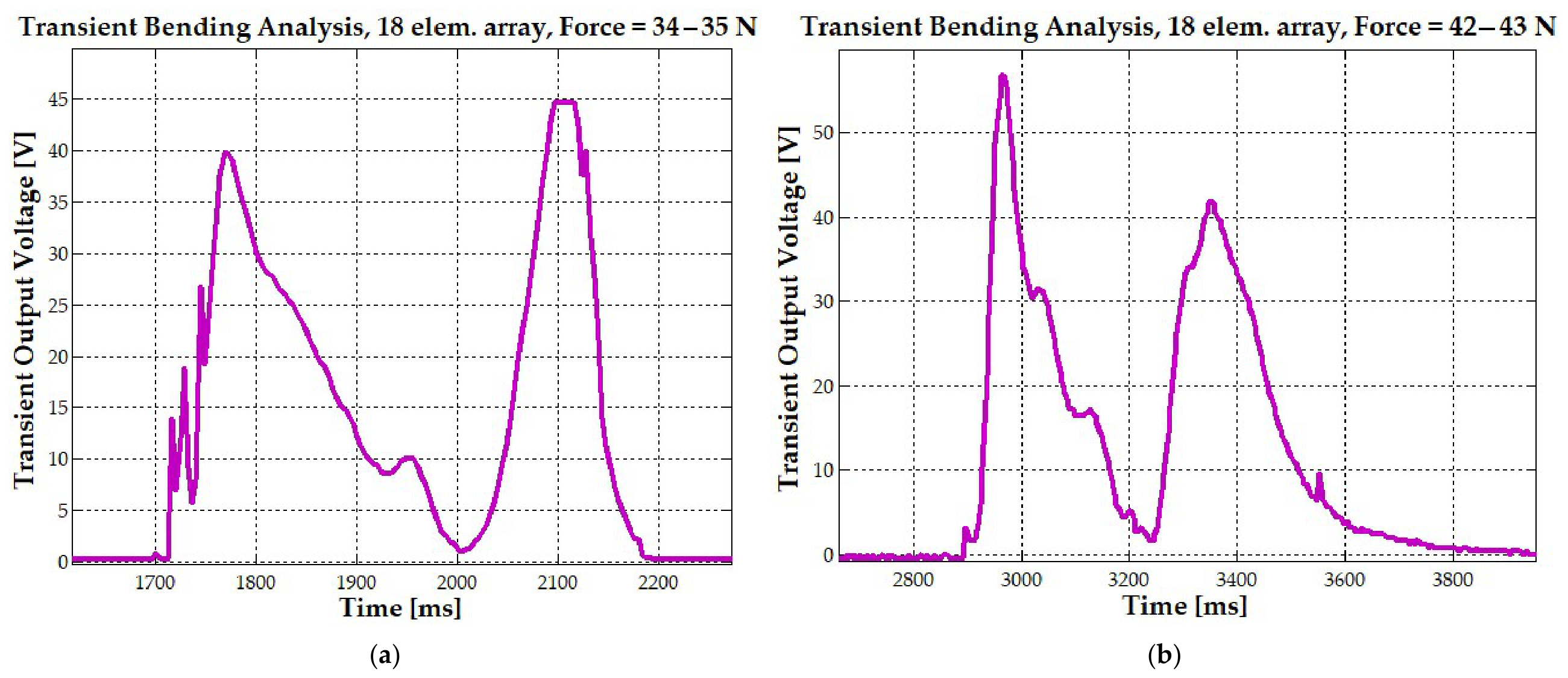
The transient voltage response of the piezoelectric generator was investigated under different manually applied pulling forces. An increase in the output voltage was observed with increasing excitation force, and these measurements were in agreement with the mean voltage values reported for the composite plate containing 18 piezoelectric elements. Voltage waveforms were recorded using a Tektronix TDS2014B oscilloscope to examine the bending and elastic recovery behavior of the plate and to determine its actuation frequency. Each acquisition captured several voltage pulses generated during repeated manual excitations at a given force level. For an applied force of approximately 22 N, the pulse amplitudes ranged from 26 V to 31 V (
Figure 8a). When the force increased to approximately 26–27 N, the pulse amplitudes increased to 31–35 V, while the corresponding actuation frequency was between 2.8 Hz and 4 Hz (
Figure 8b).
For higher bending forces in the range of 30–40 N, the voltage amplitude increased from approximately 35–40 V to 46–52 V. This trend further confirms the proportional relationship between the output voltage and the total charge generated by the piezoceramic elements. In addition, charge generation occurred during both the bending and elastic recovery stages of the plate. As a result, the charge produced during each deformation cycle passed through the rectifier bridges in two separate events, producing two positive current and voltage peaks, as illustrated in
Figure 9a,b.
For the plate incorporating 18 piezoelectric element array, an applied force of approximately 22–23 N produced a mean output voltage of 27.7 V. The corresponding standard deviation was 2.1 V, giving a relative standard deviation of 7.4%. At 26–27 N, the output voltage ranged between 31 V and 35 V. The mean value was 32.8 V. The standard deviation was 1.44 V, corresponding to a relative standard deviation of 4.4%. At 30–31 N, the maximum measured output voltage reached a mean value of 38.2 V. The standard deviation was 1.75 V, corresponding to 4.6% relative standard deviation.
For the nine piezoelectric element plate, at 29 N the mean output voltage was 22 V. The standard deviation was 0.8 V, corresponding to a relative standard deviation of 3.6%. At 36–37 N, the mean voltage increased to 26.5 V. The standard deviation was 0.88 V, corresponding to a relative standard deviation of 3.5%.
Figure 10a,b show that the bending actuation frequency remained within the range of 3.3–3.6 Hz, whereas the elastic recovery of the plate, corresponding to its return to the horizontal position, occurred within approximately 180 ms, equivalent to a frequency of about 5.5 Hz. The voltage pulses recorded by the oscilloscope are also in good agreement with the mean voltage values measured using the Fluke 2638A Hydra Series III Data Acquisition Unit, thereby validating the experimental results obtained from both measurement systems. The use of individual Schottky rectifiers allows each piezoelectric element to independently harvest energy generated during both the bending and elastic recovery phases. The rectified contributions are subsequently combined at the common DC bus, resulting in a voltage amplitude of approximately 45 V for applied forces in the range of 34–35 N and a maximum voltage amplitude of 58 V for applied forces of 42–43 N.
All results are based on mean values obtained from at least 20 repeated measurements per force level. In some cases, the number of repetitions exceeded this minimum. This was due to the need for precise synchronization between manually applied force pulses and voltage acquisition.
Manual plate bending introduced errors ranging from 3.5% to 7.4%. Forces in the range of 15–35 N could be applied relatively consistently for both plates, resulting in smaller errors 3.5–4.6%. However, when the applied force exceeded approximately 39 N, manual bending became increasingly difficult, resulting in reduced force-control accuracy. This limitation is associated with the larger displacements required from the neutral axis. In vibration-testing applications, displacement amplitudes of 50 mm and 75 mm correspond to the maximum continuous stroke (peak-to-peak displacement amplitude) of large-scale electrodynamic or mechanical shaker systems. Shakers operating within this displacement class typically provide maximum dynamic force capacities of approximately 35–50 kN. However, such force levels are far beyond the requirements of the plates investigated in this study, for which only comparatively small forces in the range of 15–50 N were applied. In addition, the tested plates would require a dedicated mechanical adaptation system for end clamping and bending, integrated with the shaker assembly.
Since the focus of this study was the assessment of the energy-harvesting capabilities of the piezoelectric plates, rather than the implementation of a complete harvesting system, a manual bending procedure was employed. This approach avoided the additional mechanical complexity associated with shaker-based excitation, whose force capacities substantially exceed the loading requirements of the tested plates. Nevertheless, the use of an electrodynamic shaker would enable precise control of both the excitation force and bending frequency.
The manual excitation frequency observed during hand actuation (approximately 3–5 Hz) corresponds to the lower range of voluntary cyclic human motion reported in biomechanics studies [
23,
24]. At these frequencies, the hand–device system approaches its mechanical compliance limit, allowing larger bending amplitudes with minimal effort.
During the transient bending event, the storage capacitor integrates all independent charge contributions on the final bus, resulting in a higher accumulated voltage for a short time after each rectifier bridge. The piezoelectric elements operate as charge sources whose generated charge is proportional to the mechanical strain. The rms voltage rise
is ultimately limited by the diode conduction condition
and the electrical load, which determine the steady operating point of the system.
The measured output bus resistance for the composite plate with 18 piezoelectric elements was . According to Equation (3), the estimated root mean square (rms) bus voltage at the maximum manual plate-bending frequency of 5 Hz was 46 V. Under the same operating conditions, a peak voltage of 62 V was experimentally measured at an applied force of 47 N. Because the harvested signal consisted of a sequence of non-uniform voltage pulses generated by manual excitation, no fixed theoretical relationship between the rms and peak voltages was assumed, and the following ratio was considered an experimentally derived parameter.
For the composite plate with 9 piezoelectric elements, the measured output bus resistance was . Based on Equation (3), the estimated bus voltage at the maximum manual plate-bending frequency of 5 Hz was 19 V. Under the highest dynamic bending conditions of 5 Hz and 41 N, the measured peak voltage reached 32 V.
From experimental measurements, an rms-to-peak voltage ratio ranging between 0.6 and 0.75 was assumed.
A composite plate containing 18 PZT elements can deliver a maximum output power of approximately 5.2 mW. The composite plate containing 18 piezo–brass disk elements could be further optimized by increasing its length to 250–260 mm and adopting a 20-element piezoelectric array. This modification would reduce the plate stiffness and decrease the coupling factor , potentially improving the overall energy harvesting performance. For a configuration with nine piezoceramic elements, the structure exhibits optimal performance when the plate length does not exceed 210 mm (analyzed case), with each element having a diameter of 20 mm and being arranged in a single row. The maximum thickness of the composite plate is approximately 1.4 mm, excluding the height of the surface-mounted Schottky diodes and the pop rivets.
Under a pulsed mechanical load exceeding 45 N, the system generates a maximum rectified voltage of 62 VDC under dynamic conditions and a rectified current of 84 µA. Measurements were performed using a Fluke 2638A Hydra Series III Data Acquisition Unit, which records the full time evolution of the voltage and current signals, allowing graphical visualization of the generated pulses. For different applied mechanical loads, the corresponding linear fitting coefficients obtained from these measurements are summarized in
Table 1.
For the plate containing 18 piezoceramic elements, measurements performed using the Agilent 34461A Digital Multimeter indicated an rms voltage of 30 V and an rms current of 180 µA when a pulsating force of approximately 45–47 N was applied. Under these conditions, the resulting maximum electrical power was 5.4 mW.
For the plate containing nine piezoceramic elements, an rms voltage of 22 V and an rms current of 108 µA were measured at an applied force of 42 N. The maximum power obtained in this case was 2.37 mW. For an average applied force in the range of 25–30 N, the generated electrical power was observed to vary between 1 and 1.5 mW.
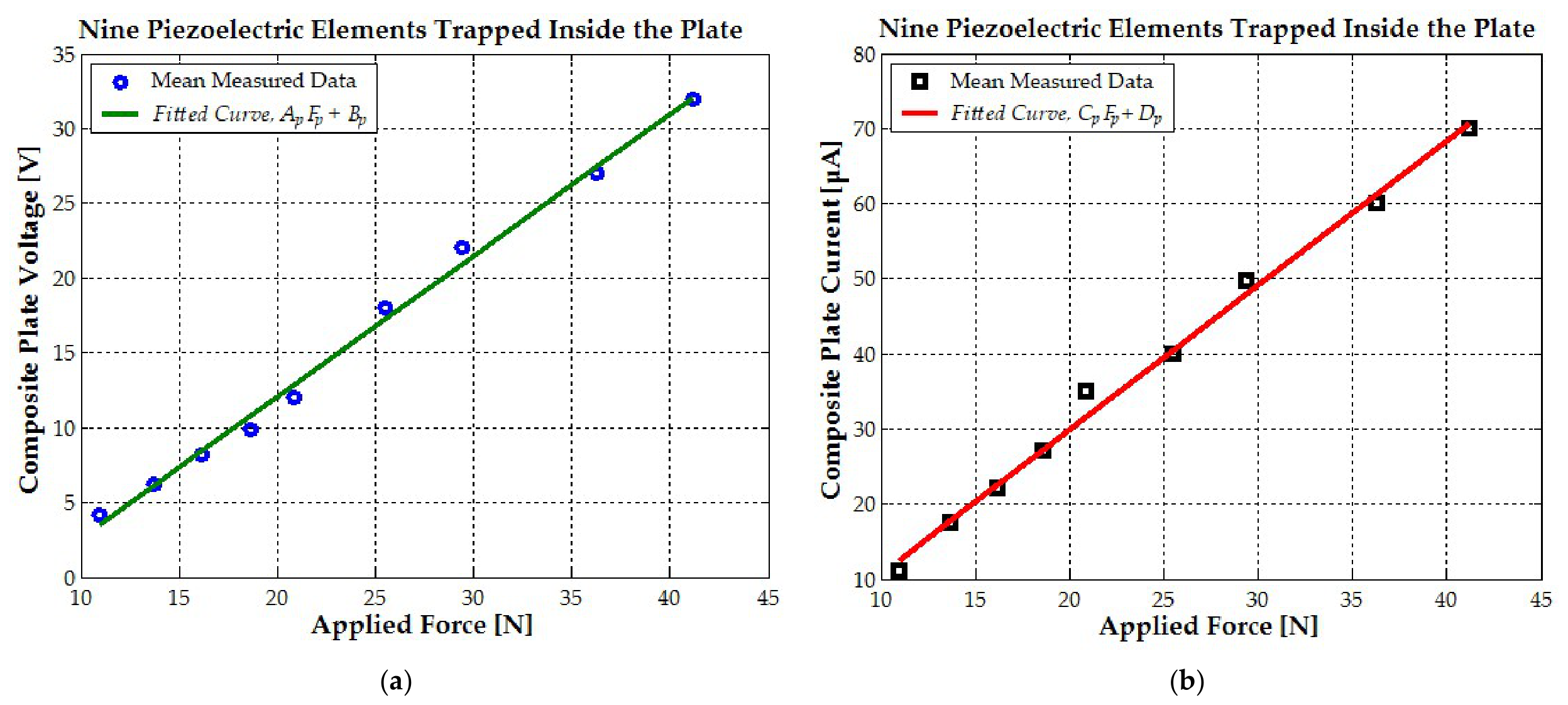
The electrical response of the piezoelectric generator was characterized under different manually applied pulling forces. The measurements indicate a clear increase in both the voltage and current amplitudes as the excitation force increases.
When a pulling force of approximately 11 N was applied on the plate containing the nine piezoelectric elements, the generated voltage pulse reached a maximum amplitude of 4.2 V, while the corresponding current pulse was about 11 µA. Increasing the force to approximately 16 N resulted in a voltage amplitude of 8.2 V and a current of 22 µA, demonstrating an almost proportional increase in electrical output with mechanical excitation (see
Figure 11a,b).
For a short excitation interval of approximately 60–80 ms, applying a pulling force of about 21 N produced a voltage pulse of 12 V and a current peak of 35 µA. This indicates that stronger transient bending of the plate significantly enhances the instantaneous electrical output.
Additional measurements further confirm this trend. For instance, forces of 13.7 N and 18.6 N generated voltage amplitudes of 6.26 V and 9.85 V, with corresponding current pulses of 17.5 µA and 27 µA, respectively. At higher excitation levels, forces of approximately 29–36 N produced voltage amplitudes between 22 V and 27 V, with current pulses increasing to 49.7 µA and 60 µA. The maximum applied force of 41 N produced a voltage pulse of 32 V and a current pulse of 70 µA. The maximum power of 2.24 mW was obtained for the plate with nine piezoelectric elements.
The experimental results demonstrate a monotonic increase in both voltage and current pulses with increasing mechanical force, confirming that the electrical output of the piezoelectric harvesting structure is strongly dependent on the magnitude of the applied mechanical excitation. The response remains consistent with the expected behavior of piezoelectric transducers, where larger bending strains lead to higher generated charge and consequently higher voltage and current pulses.
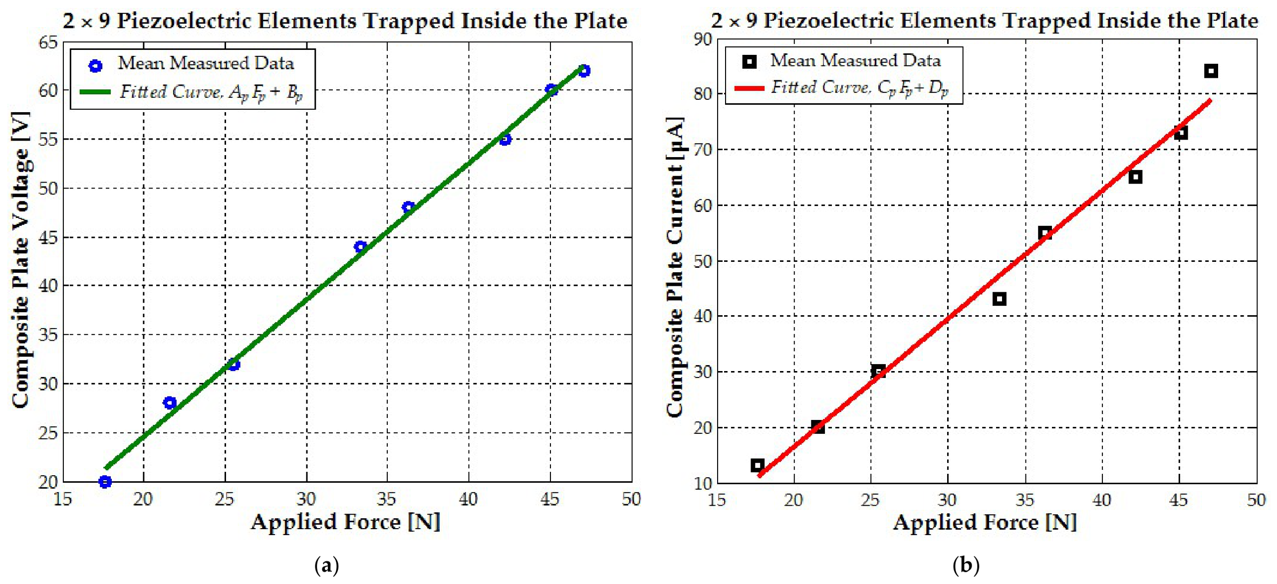
For a pulling force of approximately 17–18 N that was applied on the plate containing the 18 piezoelectric elements, the generated voltage pulse reached a maximum amplitude of 20 V, while the corresponding current pulse was around 13 µA. When the force was increased to approximately 26 N the voltage reached 33 V and the current 30 µA. At higher force levels the proportional increase becomes more pronounced. For example, forces of approximately 36 N and 42 N produced voltage peaks of 47 V and 55 V, respectively, and current peaks of 53 µA and 67 µA (see
Figure 12a,b).
Voltage and current can be further estimated from the measurements by using the linear fitted model
and
(
Table 2).
For the linear fitting voltage model of the plate incorporating nine piezoelectric elements, the coefficient of determination (R2) was 0.9948, with a linear correlation coefficient (R) of 0.997. The corresponding relative error was approximately 5%. For the linear fitting current model, the coefficient of determination was 0.994 and the correlation coefficient was 0.997, with an average relative error of about 4%.
For the plate with 18 elements, the linear fitting voltage model exhibited a coefficient of determination of 0.9972 and a correlation coefficient of 0.9986, with a low average relative error of approximately 2%. For the current model, the coefficient of determination was 0.9874, and the correlation coefficient was 0.9937, with an average relative error of about 5%. Although these errors are comparable to the relative standard deviations obtained from the measurements, the linear fitting procedure was applied to refine the mean experimental values and ensure consistency with piezoelectric theory, which predicts a linear proportionality between generated voltage and applied force through the piezoelectric coefficient d.
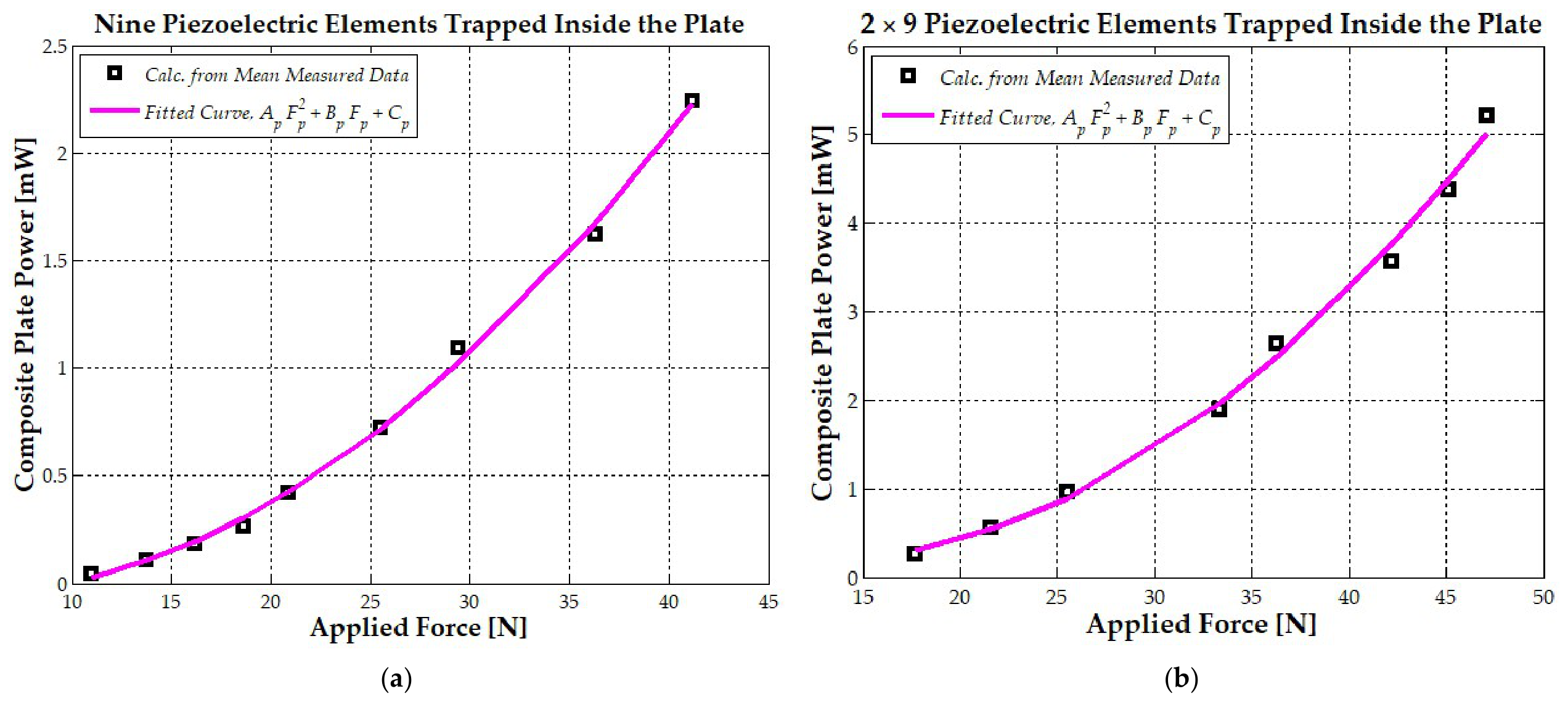
The experimental measurements indicate that the generated power increases progressively with increasing pulling force. For instance, when the applied force is approximately 11 N, the generated power is close to 0.025 mW. Increasing the excitation force to around 16 N results in a power level of approximately 0.19 mW, while for a force of about 21 N, the generated power rises to roughly 0.43 mW (
Figure 13a).
At higher excitation levels the increase becomes more pronounced. For example, forces of approximately 29 N, 36 N, and 41 N produce electrical power levels of approximately 0.98 mW, 1.64 mW, and 2.2 mW, respectively (
Figure 13a). These results confirm a clear nonlinear growth of harvested power with the applied mechanical force. Overall, the quadratic approximation captures well the observed trend and reflects the fact that stronger mechanical excitation produces larger structural deformation and consequently higher electrical energy generation in the piezoelectric harvesting structure.
Two investigations were conducted to evaluate the dependence of the generated electrical power on the applied pulling force for both configurations, the configuration consisting of nine piezoelectric elements and the one consisting of 18 piezoelectric elements. The experimental results show that the harvested power increases nonlinearly with the applied mechanical force and can be approximated by a quadratic relationship of the form:
This expression provides a good approximation of the measured data within the investigated force range. Coefficients
obtained from the experimental fitting are presented in
Table 3.
This quadratic relation (4) describes the nonlinear increase in the harvested power with the applied mechanical force. According to this model, the generated power rises from approximately 0.20 mW at 11 N to about 0.25 mW at 16 N, and further increases to roughly 0.5 mW at 21 N. At higher excitation levels the power grows more significantly, reaching approximately 1.3 mW at 29 N, 2.43 mW at 36 N, and about 3.48 mW at 41 N (
Figure 13b: 18 piezo-element structure).
Comparing the two configurations shows that increasing the number of piezoelectric elements from nine to 18 leads to an increase in the maximum harvested power from approximately 2.2 mW to about 3.48 mW, corresponding to an improvement of 63%.
For the configuration consisting of 18 piezoelectric elements, the harvested electrical power increases with the applied mechanical force and reaches a maximum value of approximately 5.2 mW at a pulling force of 47 N. This value represents the highest electrical output obtained during the experimental investigation and reflects the combined contribution of all active piezoelectric sources under strong mechanical excitation.
In comparison, the configuration containing nine piezoelectric elements produced a lower maximum power under similar excitation conditions. At the highest investigated force level (approximately 41 N), the generated electrical power reached about 2.2 mW.
The comparison between the two configurations shows a significant improvement in the maximum harvested power when the number of piezoelectric elements is increased. Specifically, the 18-element structure generates approximately 5.2 mW, whereas the nine-element configuration produces about 2.2 mW, indicating an increase of roughly 170% (about 2.7 times higher power). This improvement can be attributed to the larger number of piezoelectric transducers contributing to the total generated charge and electrical output.
Overall, the results confirm that increasing the number of piezoelectric elements substantially enhances the maximum power that can be harvested from the mechanical excitation, although the increase is influenced by the mechanical strain distribution and structural coupling within the system.
3.2. Theoretical and Experimental Investigation of the Thermoelectric Device
The aluminum tube was incorporated into the thermoelectric device to contain water or other phase-change materials (PCMs), with the purpose of maintaining the thermal gradient between the cold and hot sides for as long as possible. It is expected that further insulating the ends of the device with caps around the copper sheet, together with polyurethane foam insulation, would extend both the temperature gradient and the thermal response time of the cold side.
The first experiment described in this study was conducted to investigate heat transfer theory and thermoelectric governing equations under simplified modeling assumptions, leading to the formulation of a general coupled system of equations describing heat transfer and thermoelectric effects.
The thermoelectric device was heated to 38–40 °C using a heating blanket placed over the copper sheet. At the same time, once the hot-side temperature reached the desired level, ice-cold water (1–3 °C) or cold water (5–10 °C) was introduced into the central aluminum tube. Afterward, the heating was stopped, allowing the device to gradually cool down until thermal equilibrium was reached.
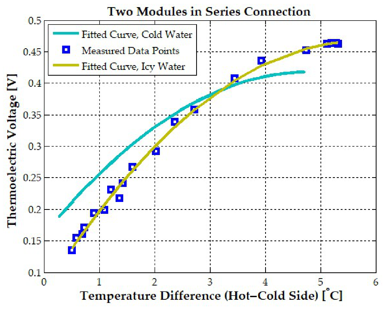
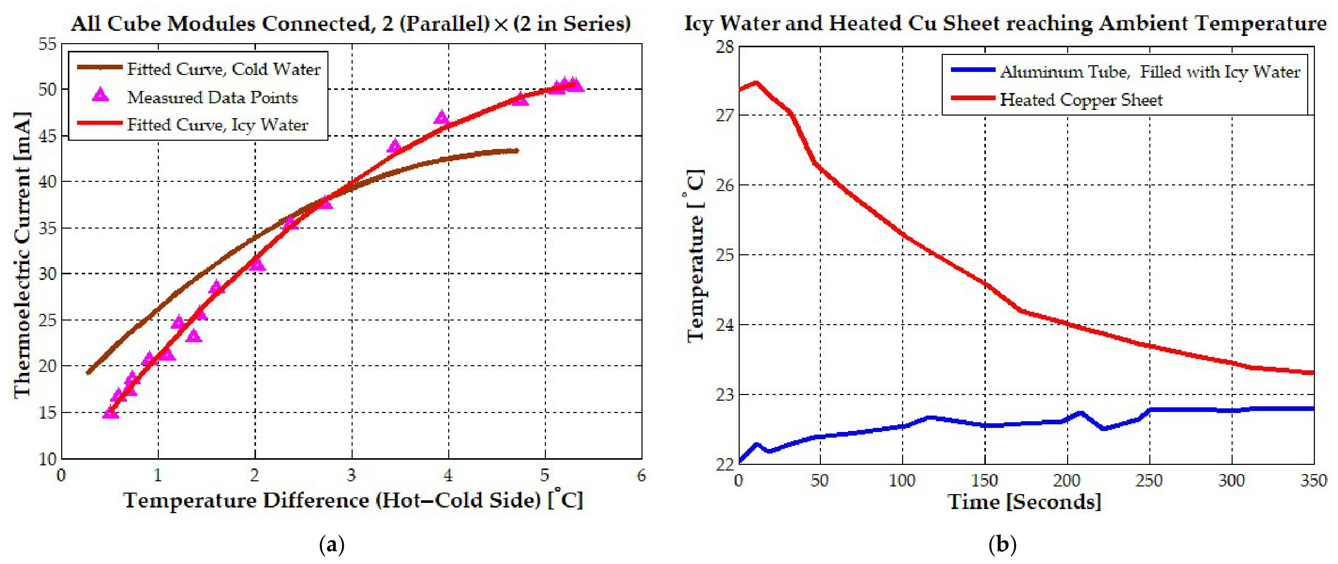
From the fitted voltage curves, it can be clearly observed that as the system cools, the temperature gradient
decreases from 5.3 K to 0.5 K when icy water is injected, and from 4.6 K to 0.7 K when cold water is used. Correspondingly, the voltage decreases from 0.463 V to 0.135 V for the icy-water case and from 0.425 V to 0.21 V for the cold-water case (see
Figure 14). The two curves intersect at approximately 3.2 K, where the voltage is about 0.39 V. At a temperature gradient of 2 K, the voltage is approximately 0.30 V for icy water and 0.33 V for cold water.
The current decreases correspondingly from 50 mA to 15 mA for icy water and from 44 mA to 21 mA for cold water. The two curves intersect at approximately 2.75 K, where the current is about 38 mA. At a temperature gradient of
, the current is approximately 31 mA for icy water and 34 mA for cold water (see
Figure 15a). For the icy-water case, the temperature gradient
decreases from 5.3 K to 0.5 K, as shown in
Figure 15b.
The equivalent thermal resistance of the system, is defined as the sum of all relevant contact thermal resistances, , the thermal resistances of the copper sheet and aluminum tube, , the water convection thermal resistance, , and the equivalent parallel thermal resistance of thermoelectric modules and .
From the above assumptions, the relation between junction temperature (between thermoelectric legs) and measured temperature can be defined as:
In general, the thermal resistances of the copper sheet and the aluminum tube are extremely small, i.e., , and may therefore be neglected in the thermal model. The thermal resistance of the aluminum tube was estimated on the basis of its geometric dimensions, namely a length of 350 mm, lateral square sides of 18.6 mm, and a wall thickness of 2.3 mm, the initial outer square side being 19–20 mm. An aluminum pipe wall thermal conduction resistance of 0.00042–0.0005 K/W was calculated considering an area of 0.020–0.027 m2. The square copper sheet (outer side 62 mm, thickness 1 mm, length 250 mm) has a large lateral heat transfer area of approximately 0.061 m2. Combined with copper’s high thermal conductivity (~400 W/m·K), which is roughly twice that of aluminum (~205 W/m·K), the resulting conduction resistance is very low, approximately 0.000041 K/W. This is about an order of magnitude lower than the corresponding aluminum case, primarily due to the higher conductivity and slightly larger effective heat transfer area.
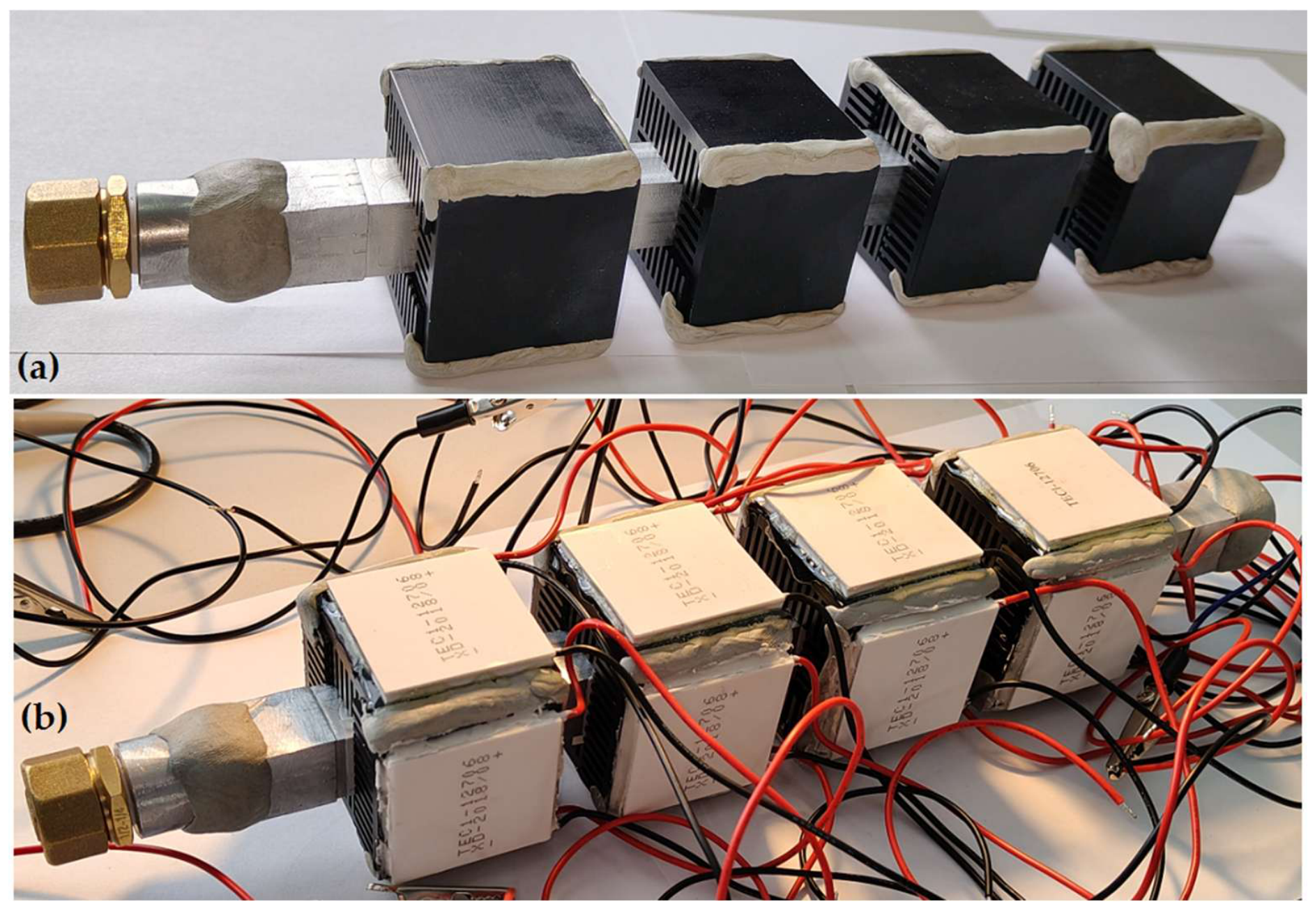
Because the heat flow is divided along parallel paths through all 16 thermoelectric plates
, corresponding to the four cubes with four active faces each, the thermal resistance of the heat sink,
, has to be added in series to the thermal resistance of each thermoelectric module,
, as expressed by the following formula:
The convective thermal resistance on the water side can be minimized by forcing the water circulation within the aluminum tube. Increasing the flow velocity enhances convective heat transfer, thereby decreasing the associated thermal resistance. For forced water convection, the thermal resistance generally falls within the range of
. However, when the water is static inside the aluminum square tube, heat transfer is governed by much weaker natural convection mechanisms, and the thermal resistance increases to approximately
. The equivalent parallel thermal resistance of thermoelectric modules is
, because the internal thermal resistance of a single thermoelectric module is
.
For both cases (static or circulating water), . In the present work, the water is static inside the pipe, so .
Parameter
can be interpreted as an external thermal feedback coefficient, which incorporates the cumulative effect of the glue-layer thermal contact, heat conduction through the ceramic layers, thermal spreading within the copper sheet and aluminum heat sink, and, most importantly, the convective heat transfer associated with the water flow. The electrical power generated within the thermoelectric module is governed by the Seebeck coefficient, the internal resistance
, and the temperature difference at the BiTe junctions,
.
The temperature coefficient of resistance is much smaller when compared to the external thermal feedback coefficient, .
Since the junction temperature cannot be measured directly, relation (7) is used to determine the junction temperature difference function of temperature gradient between the aluminum cold side and the copper-sheet hot side, temperatures were measured on both sides by attaching K-type thermocouples. If we replace the junction temperature difference,
(between cold and hot legs), with the measured temperature difference,
, between the aluminum tube and the copper outer sheet, the power relation becomes:
In order to satisfy both denominators, the equality between coefficients must be . Because , .
The global thermal feedback coefficient is a lumped, system-level parameter that quantifies nonlinear coupling between electrical transport, internal heat generation, and external thermal boundary conditions. The thermal feedback coefficient is not considered a pure material constant. The thermal feedback coefficient of the system is influenced mainly by electrical resistance growth, internal Joule heating, Seebeck nonlinearity, external thermal resistances, water convection nonlinearity and contact resistances. The thermal feedback coefficient accounts for the influence of external thermal and electrical constraints that progressively drive the system toward saturation as the temperature difference increases. In contrast, the coefficient characterizes the intrinsic power scaling, representing the quadratic dependence of output power on temperature difference as governed primarily by the Seebeck effect and the resulting thermoelectric voltage growth.
A quadratic polynomial and a first-order rational function have identical behavior up to second order if coefficients are matched. The rational form is simply a compact re-parameterization of the same local Taylor expansion. That means because , and the first order rational function is Padé 1/1 approximant only for small temperature differences,.
From
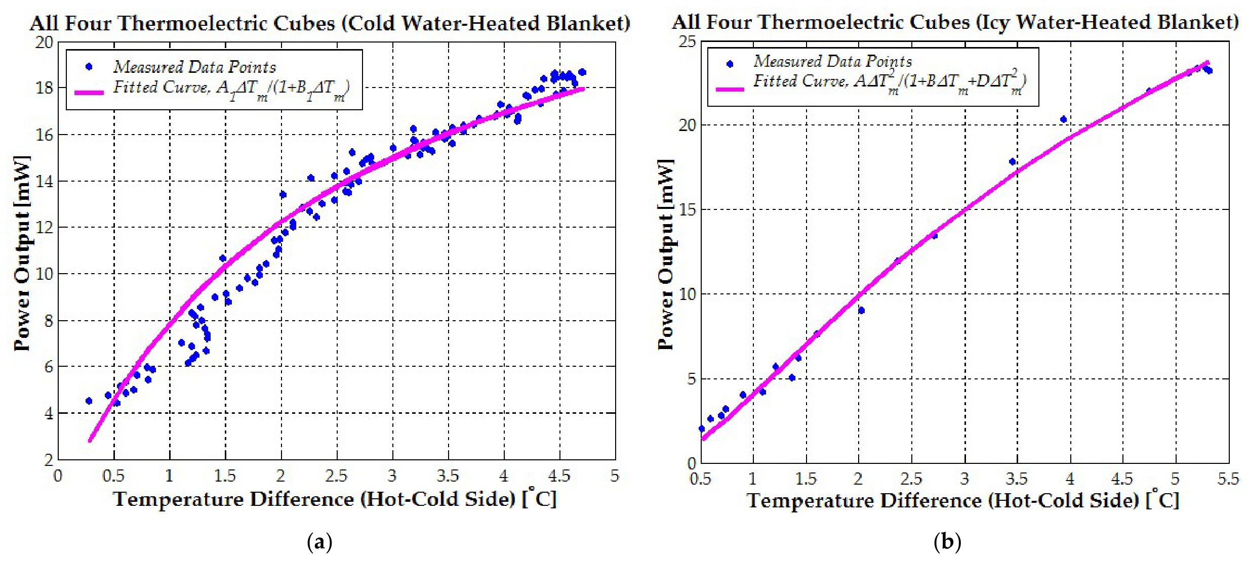
Figure 16a the first order rational function coefficients are:
. In addition, from the second graph,
Figure 16b,
,
and
, coefficients are corresponding to the second order rational function.
By substituting the above coefficient values into relation (9), taking into account the specified equalities between the coefficients, and by slightly adjusting the value of coefficient
D in order to obtain real solutions for
C, the following equation describing the device behavior is obtained.
This nonlinear rise of internal resistance and the high
external thermal resistance ratio of the entire device directly explains the saturation behavior in the power output curve, as in
Figure 16b. Since the maximum power is given by relation (9), the numerator increases quadratically with measured temperature difference Δ
Tm, whereas the denominator transitions from quasi-linear to super-linear growth beyond Δ
Tm ≈ 3 °C. Consequently, at small temperature differences, power increases rapidly due to the dominance of the Seebeck voltage term. At higher Δ
T, the accelerated growth of internal resistance offsets the quadratic voltage gain, leading to diminishing incremental power gains and the onset of saturation.
The first-order rational function depicted in
Figure 16a demonstrates a gradual decrease in power output, from 17.95 mW at a temperature difference of 4.7 °C to 16 mW at 3.5 °C, further declining to 12.2 mW at 2 °C and 7.8 mW at 1 °C.
Similarly, the cooling experiment illustrated in
Figure 16b shows a reduction in generated power from 23.7 mW, recorded at a hot-side temperature of 27.5 °C and a temperature difference of 5.3 °C, to 4 mW at a temperature difference of 1 °C.
At the midpoint of the second-order rational function, corresponding to a copper-sheet temperature of 25.5 °C and a temperature difference of 3 °C, the measured power output was 15 mW. The system required approximately 90 s of gradual cooling to reach this intermediate power level.
As a function of time, the thermoelectric device is initially heated to 38–40 °C using a heating blanket covering the copper sheet; once the hot side reaches the target temperature, cold or icy water is injected into the central aluminum tube with a graduated syringe, the heat supply is removed, and the system evolves naturally toward thermal equilibrium. Depending on the initial conditions, this evolution toward thermal equilibrium may correspond either to a cooling process or to the reverse heating process. In both cases, the temperature of the hot side is reaching the same value of 28–29 °C, due to copper sheet heat spreading after approximately 7 min.
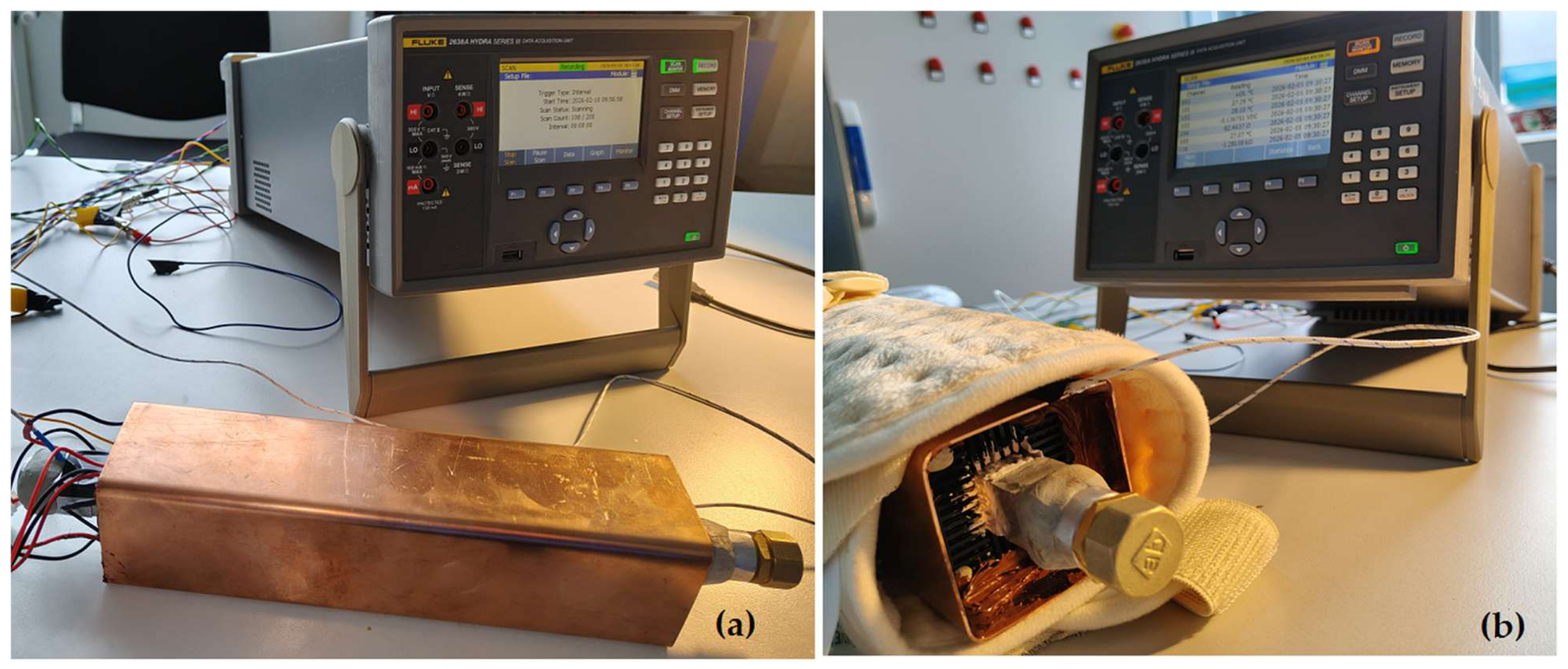
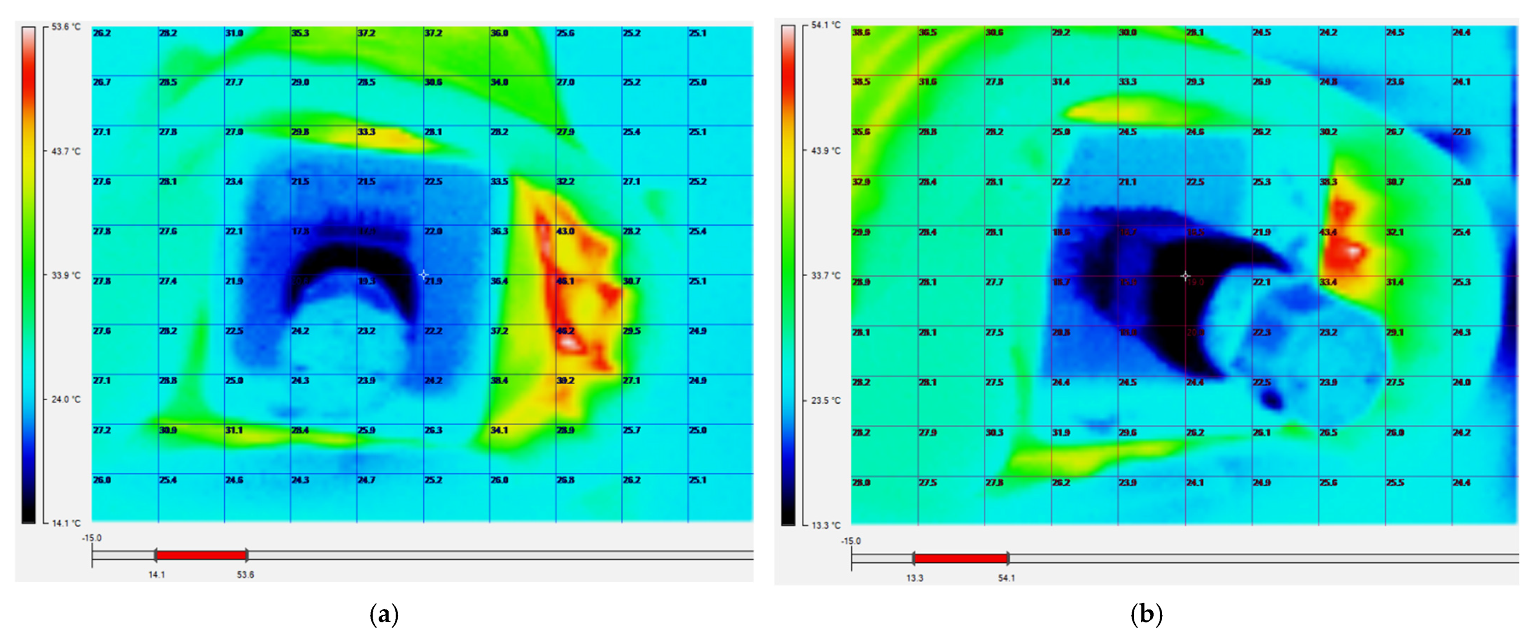
The Ti20 thermal imaging camera and the InsideIR thermal analysis software were utilized to perform an in-depth thermographic characterization of the thermoelectric heat-transfer assembly. The thermographic analysis from
Figure 17a,b revealed a strong radial temperature gradient within the thermoelectric heat-sink assembly, with temperatures ranging from approximately 15 °C at the central aluminum cooling tube to 27–31 °C near the externally heated copper surface. The heating blanket exhibited surface temperatures ranging between 38 and 44 °C, while localized regions positioned farther from the copper shell with round edges exceeded 46 °C. The outer copper sheet exhibited relatively uniform heat spreading due to its high thermal conductivity, while localized hotspots indicated regions of nonuniform thermal contact between the heating blanket and copper sheet surface.
A significant temperature drop was observed across the 4 mm thermoelectric layer, confirming effective heat transfer from the heated copper plate toward the cold-side heat sink. The thermoelectric modules established a thermal bridge between the hot external surface and the internally cooled structure, producing an estimated temperature differential of 10–15 °C across the device thickness. No abnormal heat leakage was observed through the epoxy putty or polyurethane thermal insulation separating the aluminum cubes from the thermoelectric elements, despite the possibility of parasitic heat transfer arising from their close physical contact.
The 16.5 mm heat-sink region displayed intermediate temperatures between 23 and 16 °C, demonstrating efficient thermal conduction toward the central cooling zone. While the base of the heat-sink (4 mm) showed temperatures between 21 and 23 °C, the fin structure showed progressive cooling from the fin bases to the fin tips, with temperatures decreasing from approximately 21 °C to 16–18 °C near the aluminum tube interface. This behavior indicates substantial axial heat transfer along the fins toward the cold sink.
The aluminum tube filled with icy water represented the coldest region of the system, with measured surface temperatures between 14 and 18 °C. The concentrated dark-blue thermal region surrounding the tube confirmed strong heat extraction capability and effective removal of thermal energy from the thermoelectric assembly. Overall, the thermographic field demonstrated successful inward heat transport from the heated copper shell toward the static water-cooled aluminum core, while also revealing localized asymmetries associated with thermal contact resistance and nonuniform thermal distribution. The infrared (IR) thermographic imaging is consistent with previously measured experimental data obtained for the thermoelectric device copper shell covered with the heating blanket and icy water cooling configuration. The infrared thermal analysis additionally provided the missing thermal data associated with the heating blanket, showing surface temperatures ranging between 38 and 44 °C.
As shown in the following results, heating the copper sheet while introducing cold water into the aluminum tube leads to a shorter transient time to thermal equilibrium compared with the case in which the entire device cools naturally to equilibrium with the ambient environment.
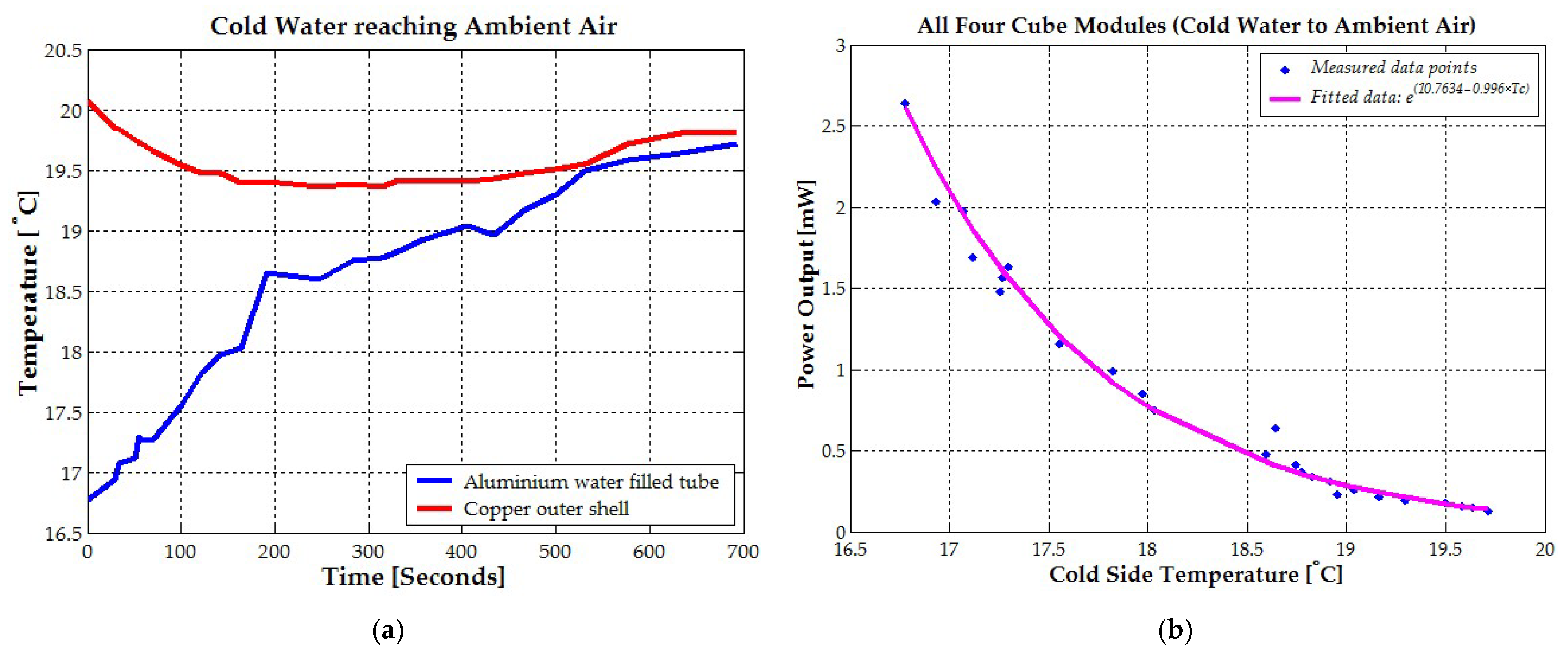
Once the hot side of the thermoelectric device stabilizes at ambient temperature (19–21 °C), a K-type thermocouple is fixed to the copper sheet and ice-cold water, at 2–5 °C, is introduced into the central aluminum tube. Following this step, the copper sheet is allowed to continue cooling until thermal equilibrium is established. Simultaneously, the temperature of the aluminum tube rises gradually from 16.5 °C to the equilibrium temperature of 19.8 °C. The experimentally measured time for this slow warming process is 11 min 33 s.
During the initial 5 min of the transient regime, the temperature difference across the device decreases from 3.3 °C to 0.7 °C. Correspondingly, the output power drops from a maximum measured value of 2.64 mW to 0.4 mW, with the cold-side temperature reaching 18.7 °C. At this point, the output voltage is only about 62 mV, and the electronic part cease to operate.
At a temperature difference
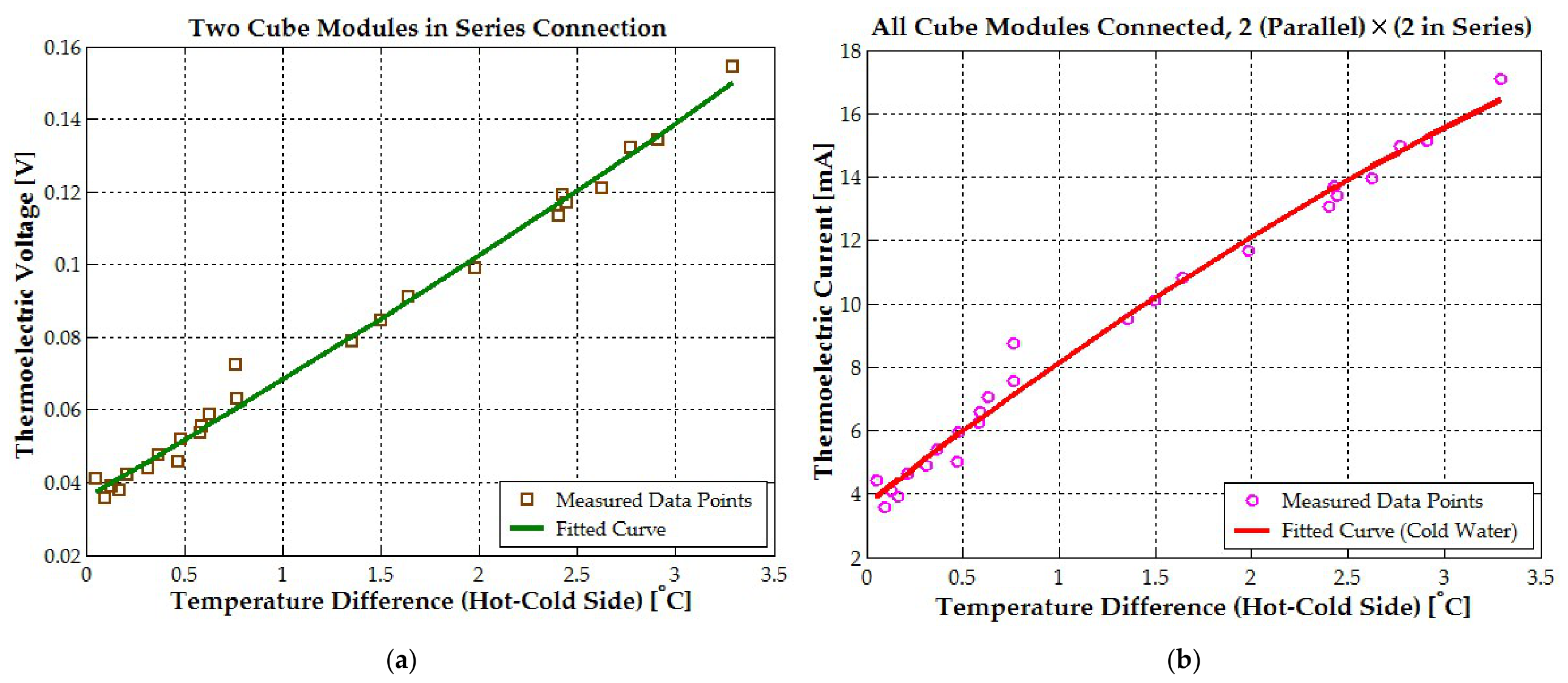
of 3.3 °C, a single cube-type thermoelectric module generated a voltage of 77 mV. Each module, as described earlier, consisted of four 40 × 40 mm thermoelectric plates connected in series. When two cube-type modules were connected in series, the output voltage increased to 154 mV, as presented in
Figure 18a. At the same temperature gradient, the measured current was 17 mA for two pairs of cube-type series modules connected in parallel (four modules).
At a reduced temperature gradient
of 2 °C, the voltage generated by each module decreased to 50 mV, while the current decreased to approximately 6 mA. As a result, for the complete arrangement of four cube-type modules connected as two series pairs in parallel, the total output voltage reached 102 mV, and the generated current was 12 mA, as shown in
Figure 18b.
At a temperature gradient of 1 °C, the measured voltage and current were 68 mV and 8.1 mA, respectively. In this case, the overall electrical power generated by the four interconnected cube-type modules was 0.55 mW, with the cold-side temperature equal to 18.4 °C.
Within approximately 100 s, the surface temperature of the aluminum tube (the cold side) increases by 1.3 °C, reducing the temperature difference to 2 °C, as shown in
Figure 19a. Under these conditions, the generated power is 1.23 mW, at a cold-side temperature of 17.5 °C. When the tube is filled with ice-cold water, the generated power remains within the range of 2.1–2.6 mW until the tube temperature reaches 17 °C. Although this time interval is relatively short, only 33 s, the maximum useful power is obtained in this case, as illustrated in
Figure 19b. Therefore, the thermoelectric device can generate an average power of approximately 2.3 mW for about 30 s solely by introducing ice-cold water into the aluminum tube, while the temperature of the hot side, represented by the copper sheet, is initially approximately equal to the ambient temperature, namely 20 °C.
The thermoelectric device is heated to 24–26 °C either by direct contact with the human body or by means of a heating blanket covering the entire copper sheet. A K-type thermocouple is attached to the copper sheet in order to monitor the hot-side temperature. At the beginning of the heating process, spring water at 10–12 °C is introduced into the central aluminum tube, as presented in
Figure 20a. The ambient temperature during the experiment is 22 °C.
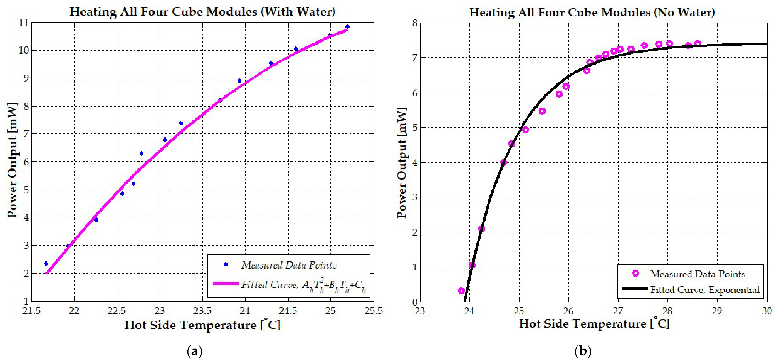
In the second experimental scenario, the aluminum tube remains empty, with no water introduced. In this case, the hot side of the thermoelectric device is initially at approximately 23 °C, close to ambient temperature, and then increases gradually under body heating to 28–29 °C over a period of several minutes, as shown in
Figure 20b. The thermal behavior observed in both experiments can be represented satisfactorily by quadratic or exponential fitting functions.
For the first heating experiment, the relationship between generated power and hot-side temperature is described by a quadratic fit of the form given by the experimental data, with coefficients , , and . According to the measurements, the generated power reaches 10.87 mW at a hot-side temperature of 25 °C, while at 22.2 °C, the measured power is approximately 4 mW.
The quadratic fit reproduces the experimental power data with good accuracy; nevertheless, it does not capture a saturation behavior, but rather represents only a maximum in the power output and a possible decline beyond that point.
In contrast, the heating experiment presented in
Figure 20b exhibits an exponential increase in generated power, as described by Equation (11). The output power increases from 1 mW at a hot-side temperature of 24 °C and approaches saturation at 29 °C, where a maximum value of 7.3 mW is obtained. At the midpoint of the exponential trend, corresponding to a copper-sheet temperature of 25 °C and an aluminum-tube temperature of 22.94 °C, the measured power output is 5 mW.
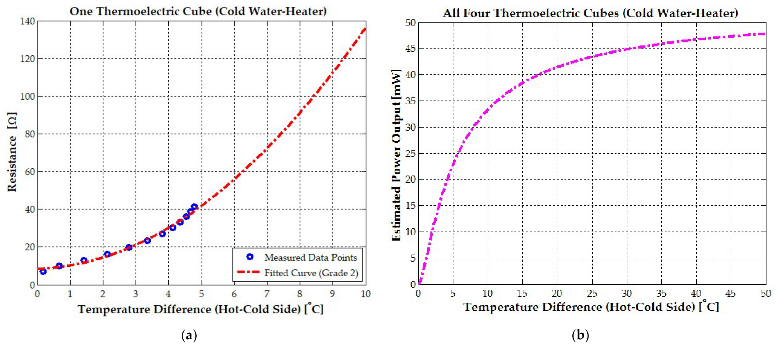
The first graph in
Figure 21a shows that the internal electrical resistance of a single cube-type thermoelectric module increases nonlinearly with the temperature difference,
. When
exceeds 3 °C, the variation can be approximated by a second-order dependence, while for very small temperature differences, in the range
, the behavior is quasi-linear. For temperature differences close to zero, the internal resistance of the complete thermoelectric cube, composed of four thermoelectric plates connected in series, ranges from 6 to 7 Ω. This arrangement is supported by the presence of the copper sheet, which provides a uniform heat distribution over all thermoelectric modules. In this case, the resistance of a single thermoelectric plate can be considered 1.6 Ω. At a temperature difference of 0.18 °C, the measured internal resistance is 7.13 Ω. The internal resistance (
) estimated from Equation (8) is approximately four times lower than the experimentally measured internal resistance of the series-connected TEC1-12706 modules of the thermoelectric cube. The quasi-linear rise in resistance, from 7.13 Ω to 19.88 Ω, is limited to the interval 0–2.78 °C. Beyond this range, the increase becomes more pronounced: between 3 and 5 °C, the internal resistance grows quadratically from 23 Ω to 42 Ω. For temperature differences above 10 °C, the estimated internal resistance reaches about 140 Ω, which significantly restricts the generated current, although the voltage output is higher.
The observed saturation in power output with increasing temperature difference is directly attributable to the nonlinear increase in internal electrical resistance (
Figure 21a,b). The same coefficients used in
Figure 16b were also applied to
Figure 21b.
The results shown in these plots are among the most relevant experimental findings, since they represent the maximum achievable temperature gradient in the proposed system, with the hot side operating near body temperature and the cold side maintained at the temperature of icy water.
The first-order rational function shown in
Figure 16a reaches saturation at approximately 25 mW, occurring at a relatively low temperature difference of 20 °C.
In contrast, the second-order rational function presented in
Figure 16b and
Figure 21b provides a more accurate fit to the experimental data, with the saturation curve stabilizing at around 50 mW for temperature differences exceeding 27 °C. Notably, the power output increases more rapidly with temperature difference up to approximately 15 °C, reaching about 38 mW. Beyond this point, the rate of power increase diminishes significantly, indicating a reduced incremental gain despite further increases in temperature difference.
As internal resistance rises with temperature difference between hot and cold side, the denominator in the power relation (9) increases sufficiently to offset the quadratic growth in Seebeck voltage, resulting in diminishing power gains and eventual saturation.
3.3. Electronic Energy Management and Storage Circuits
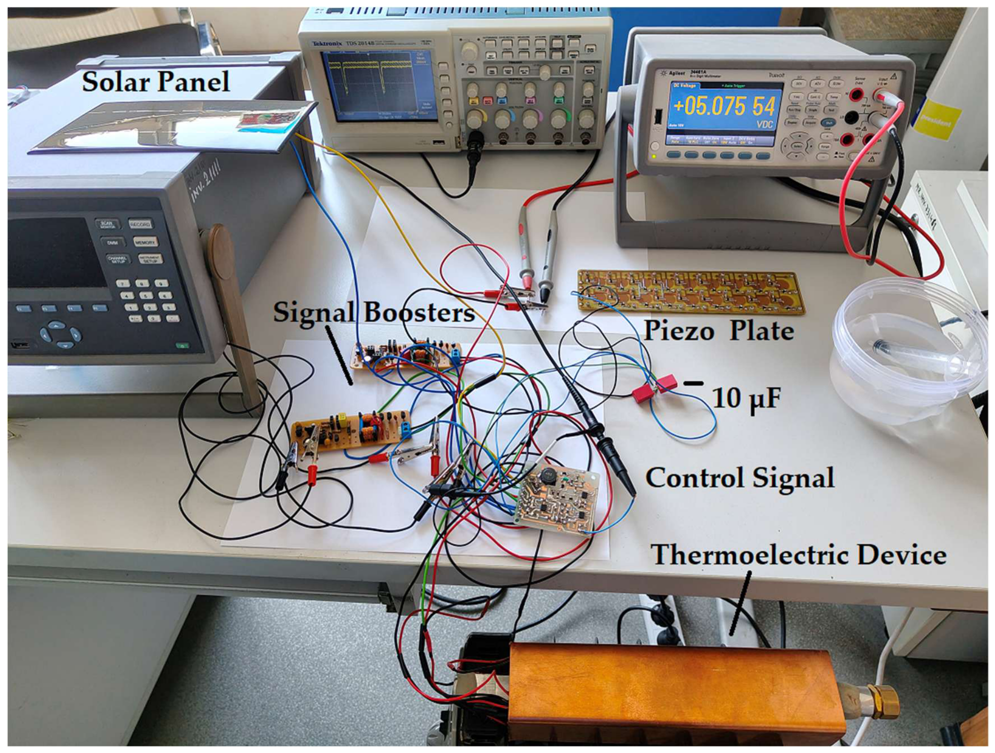
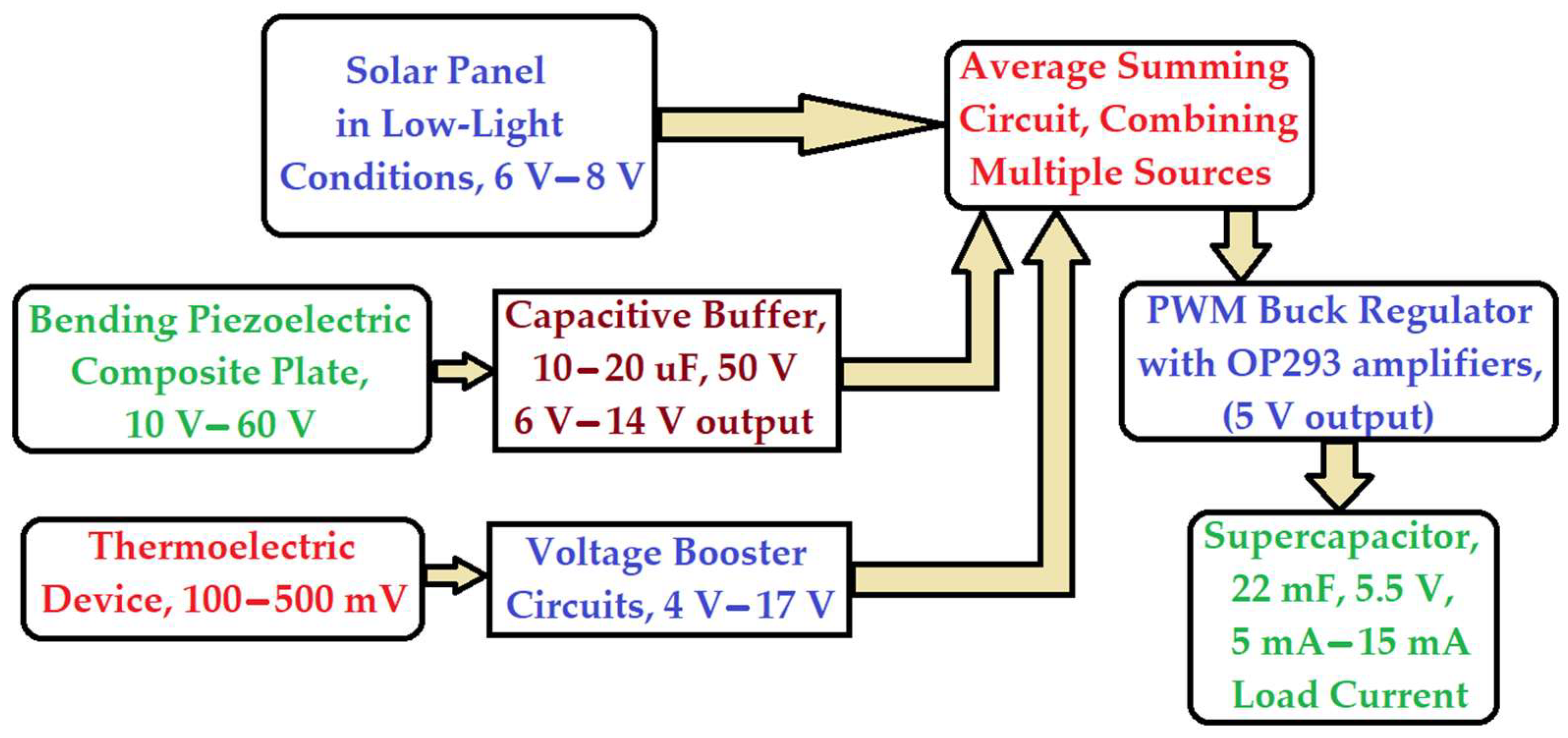
The electronic management stage was designed to combine intermittent and low-current outputs from the piezoelectric, thermoelectric, and photovoltaic sources into a regulated storage voltage suitable for supercapacitor charging (
Figure 22). The thermoelectric voltages were first increased by two Meissner oscillator circuits, each connected to a pair of thermoelectric cube modules. The boosted and rectified thermoelectric voltages were then combined with the rectified and filtered piezoelectric output and the photovoltaic contribution through a high-impedance averaging and decoupling network. This stage reduces the direct interaction between sources with different internal resistances and temporal characteristics. The resulting voltage is applied to an ultra-low-power PWM buck regulator based on OP293 operational amplifiers and a low-resistance PMOS switching transistor. The regulated 5 V output charges a 22 mF supercapacitor, while a 5.6 V low-leakage Zener diode limits overvoltage across the 5.5 V-rated storage element. This architecture allows intermittent harvested energy to be accumulated safely and converted into a more stable output suitable for low-power electronic loads [
29,
30].
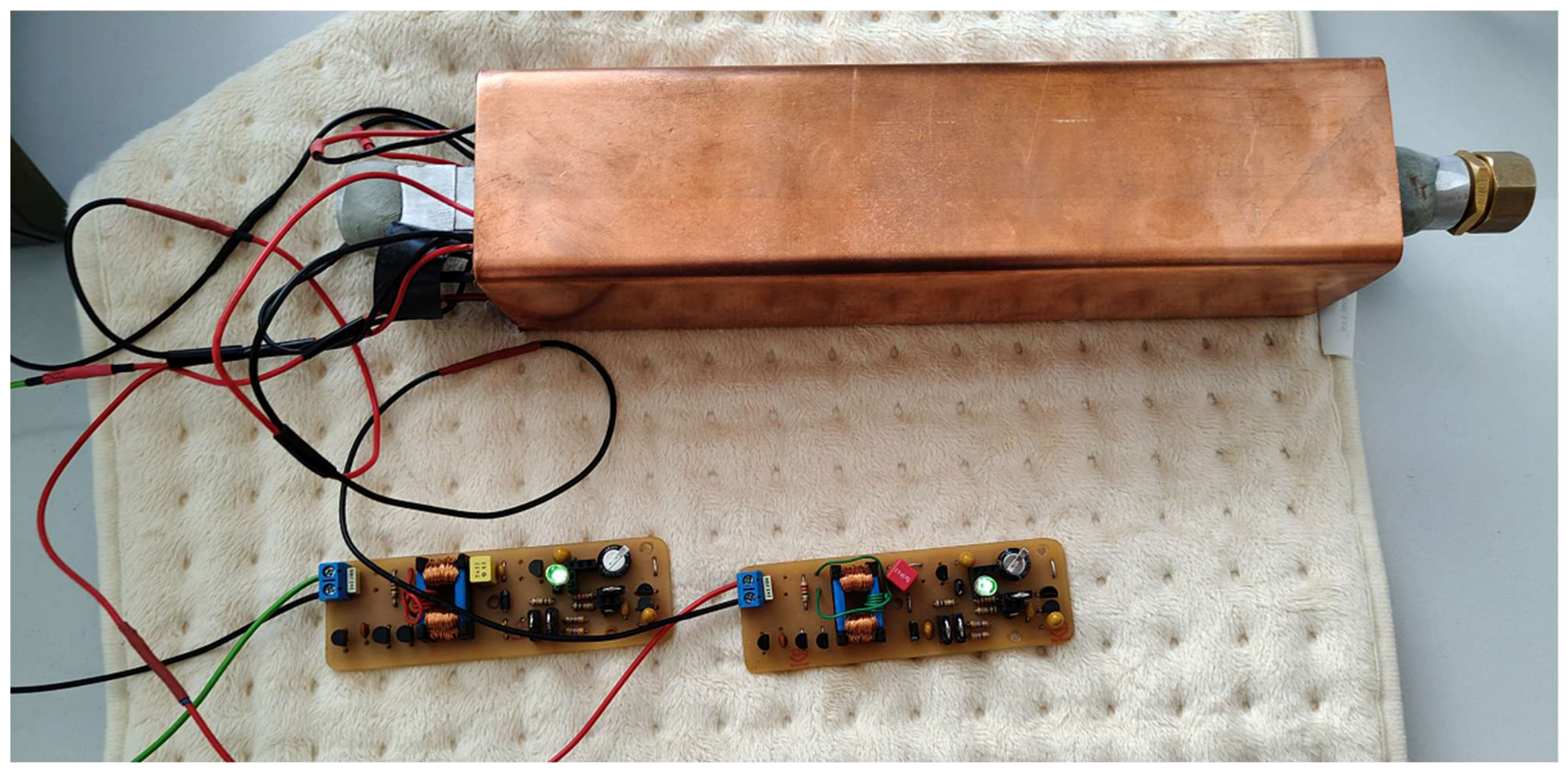
Two similar Meissner oscillator circuits were built, each connected to two TEGs placed in series on one side of the thermoelectric device. This approach was necessary because the heat delivered by the palms cannot uniformly cover the entire 250 mm-long copper sheet (see
Figure 23).
By dividing the device into two active thermoelectric sections, the available body heat could be exploited more effectively, and each TEG pair could operate under more uniform thermal conditions. The corresponding Meissner oscillator circuits were used to process independently the very low voltages generated by each TEG pair and to boost them to a level suitable for the following stage [
30]. The circuit is based on two parallel 2SK117 JFETs, used to share the input current and reduce the equivalent dynamic drain resistance, thereby limiting conduction losses, and on a BS170 MOSFET, which takes over the current once the oscillation amplitude becomes sufficiently high [
30]. Using a transformer ratio of 1:48, the circuit can raise an input voltage of 0.1 V to as much as 4 V and an input voltage of 0.48 V up to 17 V. Output voltage was measured on transformer secondary between the rectifying PMEG4005EH or SB140 Schottky diode positive side and ground. The 1–2 μF capacitor placed at the transformer secondary ensures output filtering and provides a smoother DC voltage for the power-management stage.
At peak thermoelectric power generation, corresponding to a hot-side temperature of 30 °C and a cold-side temperature of 22 °C, the circuit boosts an input voltage of approximately 0.48 V to as high as 17 V. As the device cools, the input voltage gradually decreases to 0.45 V, resulting in an output voltage of 15.4 V. With further cooling, the input–output voltage pairs reduce to 0.41 V and 14.1 V, and subsequently to 0.30 V and 10.5 V.
The thermoelectric source voltages,
and
, are derived from the secondary windings of the previously described Meissner oscillator circuits. These voltages are summed together with the piezoelectric source voltage,
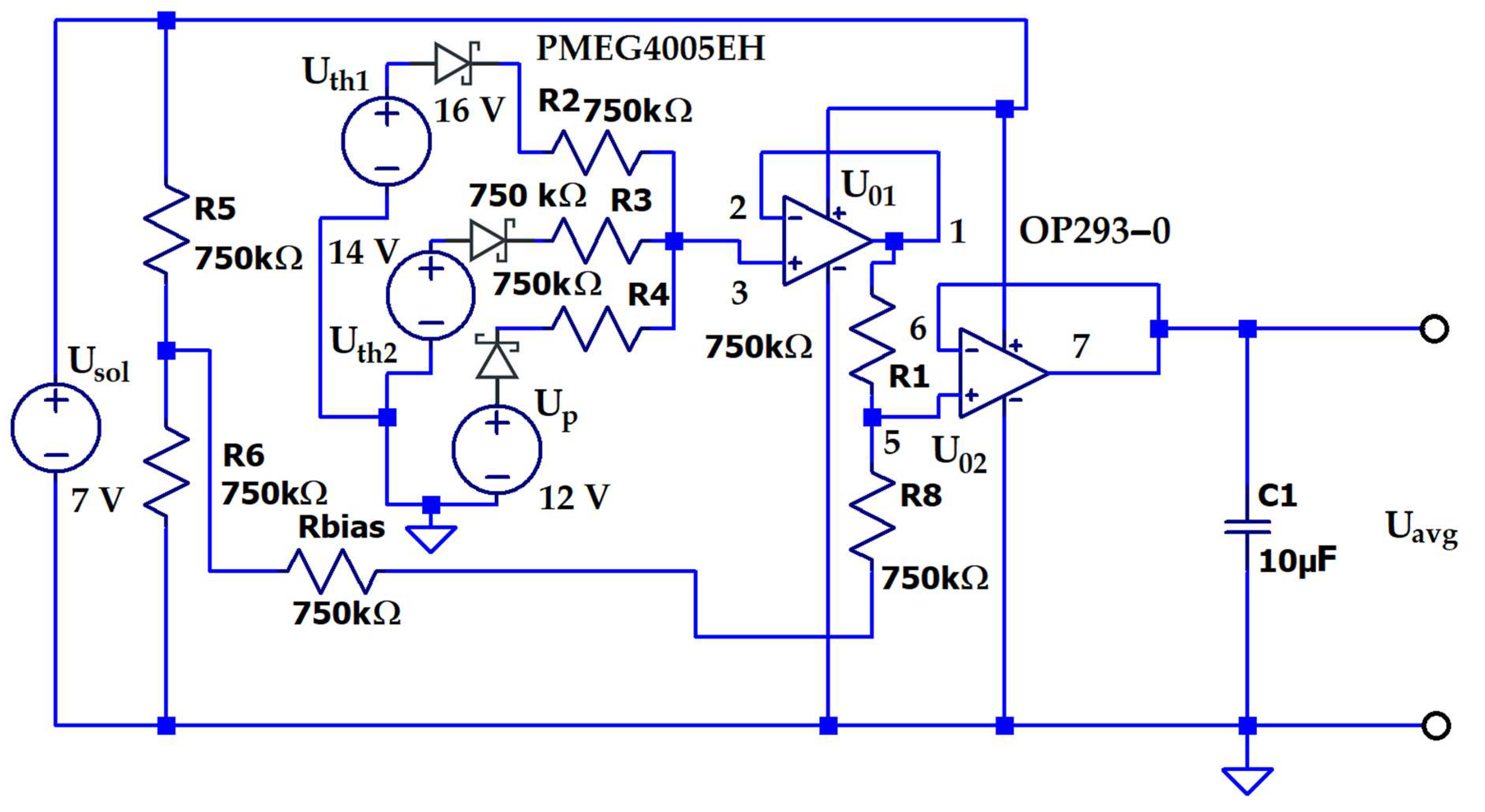
. The resulting signal, filtered by a 10 µF ceramic multilayer capacitor, represents the averaged sum of half the solar panel voltage and the individual sources contributions (
Figure 24). The electrical symbols and numerical labels in the
Figure 24 and
Figure 25 were automatically generated by LTspice software (version 24.0.9).
Both amplifiers (U01 and U02) within the Analog Devices OP293–0 are configured as voltage followers, with their inverting inputs (pins 2 and 6) connected directly to their respective outputs (pins 1 and 7). In this configuration, U02 operates as a buffer stage to ensure proper biasing and signal stability. Its non-inverting input is connected to the summing node at the output of the first amplifier (U01). Resistors R1 and R8 are used to further adjust the output voltage (if needed). Here, no further adjustments are needed, so R1 and R8 are equal. All average summing circuit resistances have the same value of 750 kΩ. From the above assumptions, the average voltage summing is defined by the following relation:
Resistors R5 and R6 establish a reference voltage (virtual ground) equal to one-half of the average solar panel voltage, . The output of the first amplifier (U01) within the Analog Devices OP293–0 is biased with respect to this reference level.
The “Star Solar” (Guangzhou) polycrystalline panel (125 × 195 mm) provides a nominal voltage of approximately 9 V at maximum power. Under full illumination conditions, it can deliver a current on the order of 300–350 mA. The corresponding open-circuit voltage is expected to exceed the nominal value.
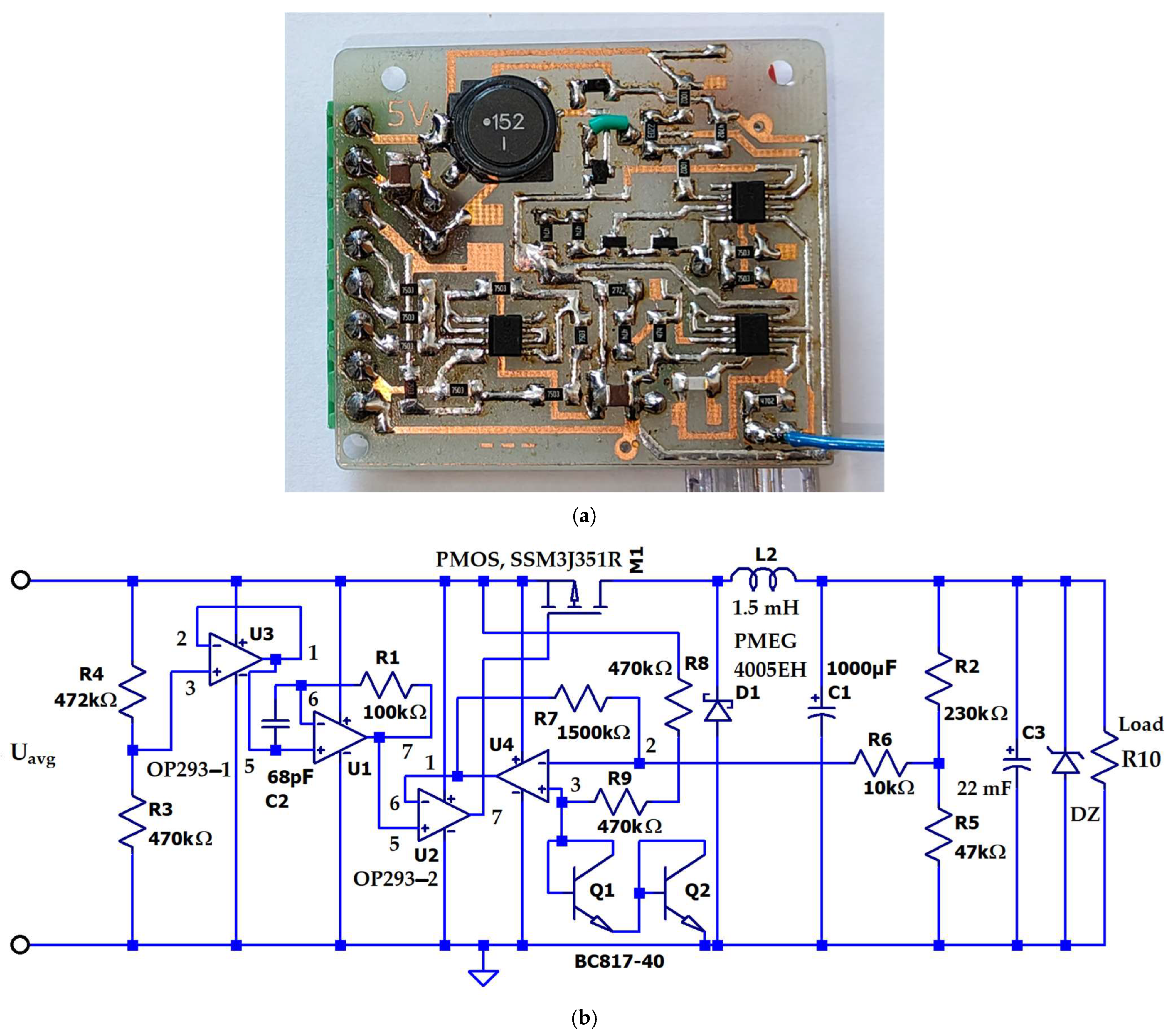
The voltage regulator circuit (
Figure 25a,b) incorporates a fully automated feedback control mechanism. It consists of a voltage follower (U3), which establishes a stable virtual ground, a quasi-triangle-wave generator (amplifier U1) that oscillates around this virtual reference (
), a PWM comparator that compares the triangular waveform with the DC control voltage corresponding to the +5 V output, and an error amplifier (U4) responsible for regulating the control signal. The comparator generates a rectangular PWM signal with an appropriate duty cycle to drive the PMOS transistor.
The reference voltage is established by means of resistors R3 and R4, forming a voltage divider that defines the virtual ground. This configuration is necessary because the operational amplifier is powered in a single-supply mode (3 V to 20 V) with respect to virtual ground, rather than in a dual-supply (differential) configuration.
Resistors R2 and R5 form the feedback voltage divider for the error amplifier. The resistor values are selected based on a feedback ratio corresponding to an output voltage of 5 V and a reference voltage in the range of 0.78–0.85 V. The upper bound of 0.85 V, corresponding to higher than 10 V input voltages, is provided by a stable reference implemented using two BC817-40 NPN transistor devices configured with their bases and collectors connected, thereby operating as diode-connected transistors. This configuration establishes a relatively constant voltage drop between the collector and emitter, which serves as the reference for the regulation loop.
The error voltage (
) is defined as the difference between the reference (target) output voltage and the feedback voltage obtained from the resistive divider. This error signal is applied to the inverting input of the error amplifier (U4) of OP293
2 integrate and is subsequently amplified according to the closed-loop gain of the inverting configuration. The gain is determined by the ratio of resistor R7 (1.5 MΩ), connected between the amplifier output and the inverting input, to the equivalent input resistance formed by resistors R2 and R5 (230 kΩ and 47 kΩ, respectively). Accordingly, the control voltage and the voltage gain of the error amplifier is given by:
The negative sign indicates the phase inversion inherent to the inverting configuration. This amplified error signal defines the control voltage used by the PWM comparator, thereby regulating the duty cycle and stabilizing the output voltage.
The quasi-triangular wave generator operates as a relaxation circuit in which the timing capacitance is referenced to a constant voltage rather than ground. The resulting waveform exhibits a predominantly triangular shape with asymmetrical characteristics: a rounded upper edge caused by an exponential charging process, and a nearly linear descending edge corresponding to a quasi-constant current during the discharging phase. The slope of the output signal
at the output of amplifier U1 is directly proportional to the current flowing through capacitor
, as expressed by:
The proposed circuit achieves quasi-triangular wave generation using a single operational amplifier U1, eliminating the need for a separate Schmitt trigger, an additional integrator stage and a non-overlapping buffer [
31,
32]. This approach results in a more compact architecture with reduced passive and active components count, thereby simplifying implementation while maintaining the required oscillatory behavior. The voltage regulator architecture incorporates four operational amplifiers. Specifically, the odd-numbered amplifiers U1 and U3, housed within the OP293–1 package, are configured to establish a stable voltage reference and synthesize the output triangle wave. Conversely, the even-numbered units, housed by the OP293–2 package, function as a comparator (U2) and an error amplifier (U4), respectively. Within the comparator stage, the triangle wave is modulated by the DC feedback signal to generate a pulse-width modulated (PWM) waveform with the requisite duty cycle [
33]. This duty cycle is dynamically adjusted based on the input-to-output voltage ratio; for instance, given an input of 15 V and a target output of 5 V, the switching transistor operates with a 25% conduction interval and a 75% cutoff period. A similar proportional adjustment, of 50%, occurs for a 10 V to 5 V conversion.
The supply current per amplifier is limited to a maximum of 30 µA. Consequently, for three Analog Devices OP293 units—comprising a total of six amplifiers—the maximum current consumption is 180 µA. This current budget accounts for both the average summing voltage circuit and the 5 V buck regulator. All resistive elements were carefully selected to minimize current flow, with operating currents constrained to the range of a few microamperes, typically between several µA and 12 µA, and not exceeding 20 µA. As a result, the combined current consumption of the averaging (summing) stage and the voltage regulation (control) circuitry remains below 300 µA. For comparison, conventional PWM drivers or integrated buck regulators such as LM25017 [
29] typically exhibit supply currents on the order of 1–10 mA, highlighting the efficiency of the proposed design. The control circuitry (command block) consumes approximately 1.9 mW of power.
For applications requiring low supply and load currents, typically in the range of 1 to 200 µA, while maintaining operation at high switching frequencies, conventional discrete buck converter implementations become inefficient or impractical. In such regimes, parasitic effects, switching losses, and control overhead can dominate overall performance. Therefore, specialized buck converters must be monolithically integrated on-chip and carefully optimized for ultra-low-power operation [
34,
35,
36]. These integrated designs often employ techniques such as pulse-frequency modulation (PFM) or hysteretic control instead of traditional pulse-width modulation (PWM), as they reduce switching activity and associated losses under light-load conditions. Additionally, on-chip integration minimizes parasitic inductances and capacitances, which is critical at high frequencies, where such non-idealities significantly impact efficiency and stability.
Furthermore, the use of high switching frequencies enables the reduction of passive component sizes, particularly inductors and capacitors, facilitating full or partial integration within the silicon die or package [
37].
In the power stage, a current of 9–10 mA flows through the coil. Under these conditions, the power dissipated across the 1.9–2 Ω internal resistor is approximately 240 µW, while the conduction losses in the PMOS transistor are approximately 12 µW (0.1–0.12 Ω on resistance), corresponding to a load power transfer of about 46 mW. Based on the experimental data, it can be concluded that a total power loss of approximately 3.5–5 mW occurred within the energy management stage. Given an input power of 50 mW, this corresponds to an efficiency of at least 90% for the core of energy management circuit.
This system implements a high-efficiency buck converter designed for energy harvesting from solar (7 V), thermoelectric (14 V and 16 V) and piezoelectric (12 V) sources regulated via an OP293 ultra-low-power operational amplifier. The architecture utilizes a voltage-follower and an average summing input stage for source decoupling, feeding a PWM comparator that modulates an SSM3J351R P- MOSFET drain to source channel with Rds_on = 0.1 Ω. Although the average input current is only 2–3 mA, the converter maintains a stable 5 V output, even under an inductor ripple current of over 10 mA.
The discrepancy between the low source current and high ripple current is attributed to the Discontinuous Conduction Mode (DCM) of operation [
36]. The oversized 1.5 mH inductor (rated for 500 mA) acts as a high energy reservoir, while the 1000 µF output capacitor effectively filters the audible frequency signals (situated between 3 and 10 kHz). This configuration ensures that the average power delivered by the high-impedance sources is sufficient to maintain regulation, with the inductor ripple being largely reactive and contained within the output filtering stage.
Efficiency is maximized by leveraging the OP293’s microampere current, which prevents the control circuitry from exhausting the limited energy delivered by the harvesting sources. The use of a low-threshold MOSFET (Vth = 0.8 V) ensures reliable switching even at low input potentials. To protect the connected Panasonic Gold Capacitor (GC) type supercapacitor rated at 5.5 V (GC5.5V.022F), having an internal equivalent series resistance lower than 75 Ω (ESR), a low-leakage Zener diode of 5.6 V (MMSZ4690 from Vishay) is connected in parallel to prevent overvoltage conditions during transient load changes, ensuring long-term reliability of the energy storage components. The PMEG4005EH Schottky barrier rectifier diode, manufactured by Nexperia, is designed for efficient rectification in low-power applications. It supports a maximum repetitive peak reverse voltage of 40 V. A key characteristic of this diode is its exceptionally low forward voltage drop, typically ranging from 0.1 V to 0.15 V at forward currents between 0.1 mA and 1 mA. This low forward voltage contributes to reduced conduction losses and improved efficiency, particularly in energy-sensitive or low-current circuits. Because the typical junction capacitance of the PMEG4005EH diode is on the order of tens of picofarads, and due to the absence of reverse recovery effects, the device is capable of high-speed operation, with practical maximum operating frequencies on the order of MHz.
The BAS40-04 Schottky diode array, comprising two Schottky diodes connected in series, exhibits a low forward voltage drop of approximately 0.15–0.20 V per diode at the operating current range of 7–12 µA generated by each piezoelectric element under applied forces of 41–47 N. Since each full-bridge rectifier consists of four diodes, the power dissipated in a single rectifier is approximately 6 µW. Consequently, for the composite plate incorporating nine piezoelectric elements, nine full-bridge rectifiers are required, resulting in a total rectification loss of approximately 54 µW. Similarly, for the composite plate incorporating 18 piezoelectric elements, 18 full-bridge rectifiers are employed, leading to a total rectification loss of approximately 108 µW.
At the highest investigated force level of approximately 41 N, the composite plate containing nine piezoelectric elements generated a maximum electrical power of about 2.2 mW. Accounting for the rectification losses, the corresponding power conversion efficiency was approximately 97–98%. Likewise, for the configuration containing 18 piezoelectric elements, the generated electrical power reached approximately 5.2 mW at the highest investigated force level of about 47 N. With rectification losses of 108 µW, the overall efficiency remained close to 98%.
The thermoelectric source delivers a maximum input power of 25 mW to a Meissner oscillator-based resonant conversion stage, which also functions as a voltage and signal (booster) conditioning circuit. Within this stage, dissipative losses associated with active switching devices (BS170 MOSFETs/2SK117 JFET biasing network) and transformer core and copper losses are estimated in the range of 6–9 mW. Consequently, the net power delivered to the load is approximately 16–19 mW, corresponding to an overall electrical conversion efficiency of 64–76% for the Meissner oscillator circuit under the specified operating conditions. If the previously calculated efficiencies are multiplied, 0.98 × 0.90 × 0.69 ≈ 61%, which is the overall (rough system-level estimate of) typical electronic-path efficiency.
The regulated 5 V output was connected to one of the two 22 mF supercapacitors. Under these conditions, both the supercapacitor and the 1000 µF electrolytic capacitor at the output reached full charge (at 5 V) in approximately 100 s. The 1000 µF electrolytic capacitor alone charged within 15–20 s, depending on the current supplied by the energy sources. The experimental results indicated that the supercapacitor reached approximately 2 V within 25–30 s and approximately 4 V after 1 min of charging.
The analysis considers an optimal operating scenario in which the combined contribution of thermoelectric, piezoelectric, and photovoltaic sources yields a total power output of approximately 43–45 mW. Prior experimental investigations on the thermoelectric subsystem demonstrated that four thermoelectric cube modules can generate between 20 and 25 mW. The photovoltaic source contributes at least 14 mW under natural daylight conditions, including cloudy skies, where an open-circuit voltage of approximately 7 V and a maximum current of 2 mA were measured.
However, the thermoelectric modules exhibit limited current output. Specifically, two thermoelectric cube modules connected in series produce approximately 600–700 µA at 17 V (measured at the output of the Meissner oscillator circuit). This current level is insufficient to directly supply the voltage regulator and the averaging summing circuit. To mitigate this limitation, the photovoltaic source provides a continuous and relatively stable power contribution, even under suboptimal illumination conditions.
Due to their inherently low current output, the thermoelectric and piezoelectric sources alone are unable to sustain a stable input voltage; the voltage rapidly drops below 5 V, causing the voltage regulator to cease operation (see
Figure 26). Conversely, the photovoltaic source alone is also insufficient to maintain regulator functionality, due to the 3.5 V reference threshold observed under low-irradiance conditions. This configuration was therefore selected to demonstrate the feasibility and versatility of the averaging summing circuit in integrating multiple low-power energy sources with complementary characteristics.
The regulated output voltage of the converter dropped below 4.8 V only when the input power was insufficient (below 15 mW). For input power levels between 20 mW and 50 mW, the regulator maintained a stable output voltage in the range of 4.9–5.1 V. The output voltage was measured using an Agilent 34461A Digital Multimeter, while control signals were monitored with a Tektronix TDS2014B Oscilloscope.
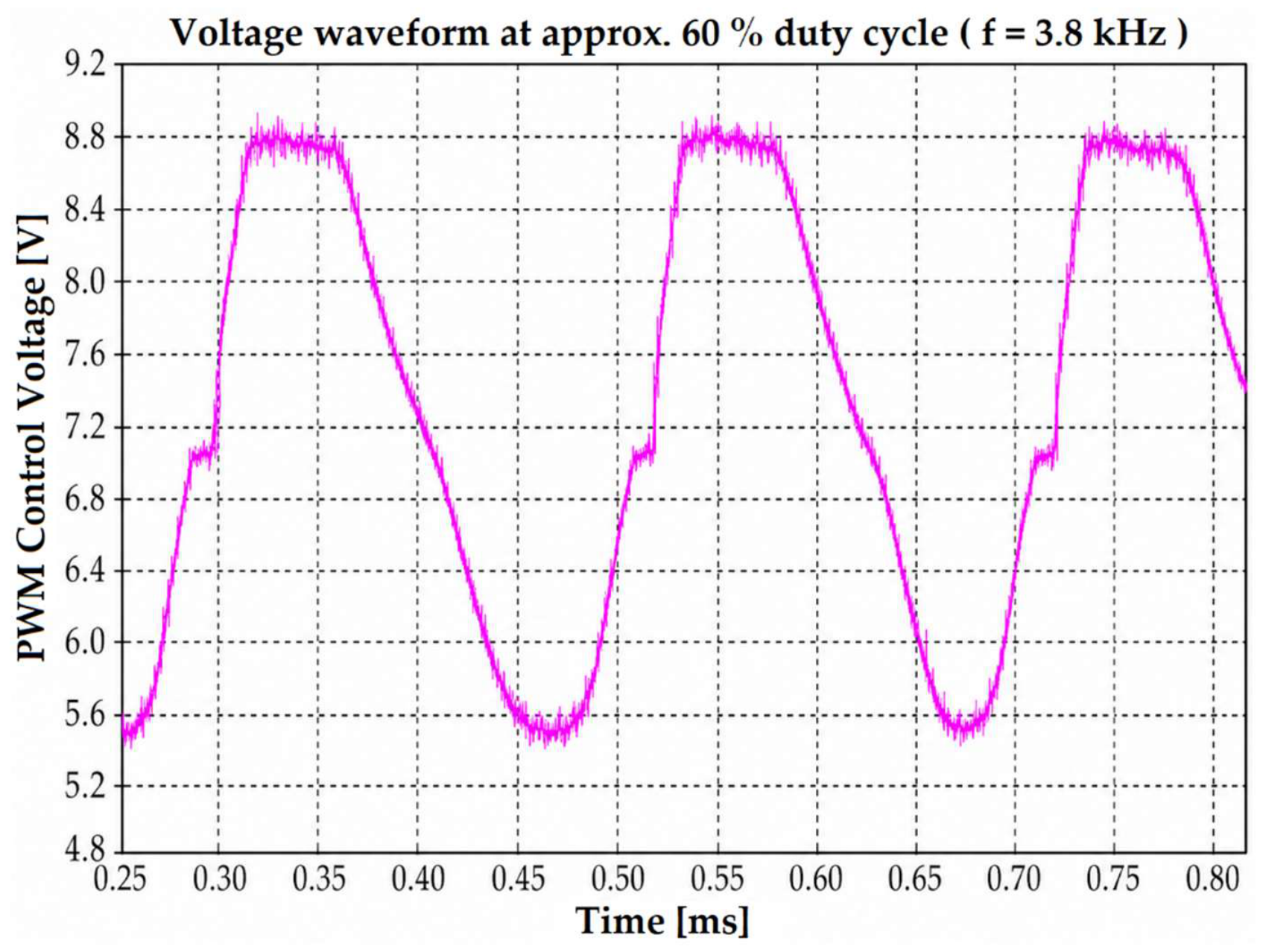
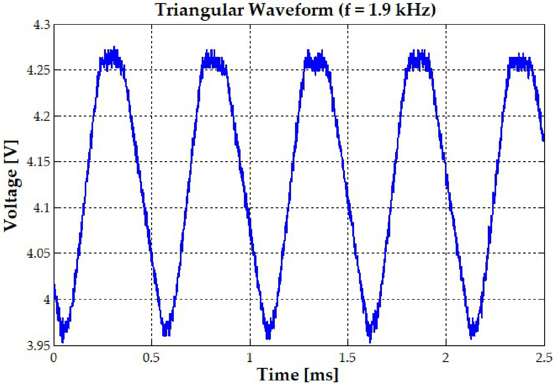
The ~60% duty-cycle PMOS gate control signal and the triangular carrier waveform were measured using a Tektronix TDS2014B Oscilloscope (see
Figure 27 and
Figure 28). The triangular waveform was recorded after the duty cycle was established. During this interval, the thermoelectric and piezoelectric sources exhibited a slight decrease in voltage and output power, with the combined input voltage dropping from 8.8 V to 8.2 V.
In PWM-based control, a triangular carrier waveform is compared with the feedback voltage derived from the regulator output to generate a rectangular switching signal, with the duty cycle governed by the input-to-output voltage ratio (for a buck converter duty cycle
). The waveforms from
Figure 27 and
Figure 28 were acquired under operating conditions in which the thermoelectric voltage boosters produced approximately 10 V each, the piezoelectric bending plate delivered about 12 V after the 20 µF buffer capacitor, and the solar panel generated approximately 7 V under low illumination. Based on (12), the resulting combined voltage at the regulator input was 8.8 V. The triangular carrier waveform operated in the range of 1.9–2 kHz, while the comparator output signal used for gate drive exhibited a frequency of approximately 3.8–4 kHz. This relationship is consistent with the expected behavior of comparator-based PWM generation, where two switching events occur per carrier period. The output feedback voltage was maintained around 4.15 V, positioning it well within the carrier amplitude range (3.95–4.27 V), thereby ensuring a stable duty cycle (approximately 60–65%) and reliable switching operation with adequate noise margin.
Traditional buck converter architectures often struggle with the trade-off between sensing complexity and dynamic performance. To address this, recent advancements propose novel control schemes employing dual-loop mechanisms that decouple switching frequency from output regulation [
38,
39]. For instance, by utilizing a constant switch-ON time alongside a variable switch-OFF time modulated by output voltage feedback, these systems achieve superior transient response and faster stabilization.
The OP293 integrated circuit can be replaced with the TSV912 in applications where enhanced dynamic performance is required. This substitution enables a significantly improved transient response, primarily due to its higher slew rate (increasing from 0.3–1 V/µs to 5–8 V/µs) and the ability to operate at higher frequencies in the range of 50–100 kHz. However, this performance gain comes at the expense of increased power consumption, with the supply current rising to approximately 0.8–1 mA per amplifier, representing the principal design trade-off in the design decision.