1. Introduction
With the rapid development of third-generation semiconductor materials, surface acoustic wave (SAW) devices have been extensively applied in communications [
1], automotive electronics [
2], aerospace [
3], medical diagnostics [
4], chemical analysis [
5], and sensing applications [
6,
7,
8,
9,
10]. However, with the advent of the big data era and the increasing complexity of detection environments, high-performance SAW devices featuring a high electromechanical coupling factor (
K2) and low insertion loss (
S21) have garnered significant attention [
11]. At the device level, the
K2 is an indispensable parameter for characterizing high-performance SAW devices, as it directly determines their sensitivity and bandwidth. A higher
K2 facilitates greater energy conversion efficiency, faster response speeds, wider bandwidths, and superior sensitivity. Consequently, enhancing
K2 has emerged as a primary research focus for the development of high-performance SAW devices [
12].
Currently, doping is a widely adopted method for enhancing
K2. This technique modifies the piezoelectric layer of SAW devices by introducing metal ions, such as V or Al. Fu et al. [
13] doped V ions into the ZnO piezoelectric layer of a ZnO/SiC device, increasing the
K2 from 2.8% to 5.12%. Similarly, Iborra et al. [
14] compared the piezoelectric properties of pure ZnO and Al-doped ZnO (AZO), finding that AZO exhibited an increase in
K2 from 0.044% to 0.069% compared to conventional ZnO. However, doping methods do not consistently enhance piezoelectric performance and can sometimes lead to a reduction in
K2. For instance, Ralib et al. [
15] observed that doping AlN piezoelectric films with V ions did not enhance
K2, but rather reduced it by 1.2% compared to the conventional structure. Alternatively, the superposition method, which involves stacking additional materials onto the piezoelectric layer to form multilayer structures, offers another approach to enhancing
K2. Luo et al. [
16] utilized (110)-oriented ZnO to create a three-layer SAW device structure, achieving a high
K2 of 3.37%. Shen et al. [
17] proposed a multilayer SAW structure (a-ZnO/a-GaN/r-sapphire) capable of reaching a maximum
K2 of 7%. However, this stacking approach relies heavily on precise material selection and crystal orientation control, which significantly increases manufacturing complexity. In recent years, piezoelectric layer etching has garnered significant attention due to its effectiveness and simplicity. Dun et al. [
18] proposed a Ni/etched-ZnO/Si structure using Ni as the conductive material; by etching the piezoelectric layer, the device achieved a
K2 of 4.26%. Furthermore, Dun et al. [
19] modified the conductive material to propose a patterned Al/ZnO/Si structure, attaining a maximum
K2 of 7.98%, approximately seven times higher than that of conventional structures. Xu et al. [
20] introduced a ZnO/SiC hierarchical structure with etched piezoelectric layers. By optimizing the piezoelectric film thickness, electrode parameters, metallization ratio, and etch ratio,
K2 was increased to 12%, nearly twelve times that of the unetched structure. Fan et al. [
21] proposed a Lamb wave resonator with a trapezoidal groove configuration, demonstrating that by adjusting the etching depth, the
K2 could be enhanced to 5.47% without compromising the overall device performance. Similarly, to improve the electromechanical coupling, Fan et al. [
22] designed a four-layer IDT/etched-AlN/IDT/AlN/diamond resonator, achieving a
K2 of 3.09%. Furthermore, Liu et al. [
23] investigated the variation of
K2 in an AlN/Sapphire structure subjected to trapezoidal etching. Their results revealed that the etched configuration yielded a
K2 of 6.8%, representing a two-fold increase compared to its unetched counterpart. Based on the aforementioned studies, it is evident that although the etching method can effectively enhance the
K2 of SAW devices, this improvement still exhibits certain limitations. Specifically, under the premise of maintaining other optimal device parameters, the maximum reported
K2 is merely limited to 12% [
20]. Therefore, there remains substantial room for further optimization of the etching strategy.
To design SAW devices with a high electromechanical coupling factor, this paper utilizes coupling theory to thoroughly analyze the interaction mechanism between mechanical energy and the electric field. Specifically, the analysis focuses on the limitations inherent in conventional Al/ZnO/Si structures, which stem from mechanical energy leakage and the spatial mismatch between the mechanical and electric fields. To address these challenges, a trapezoidal etching structure was proposed and simulated using the finite-element method (FEM). By varying the bottom width (SZnO), under Rayleigh mode, the variation characteristics of K2 and wave velocity (VP) with the thickness of the piezoelectric material (HZnO) and different etching ratios (dZnO/HZnO) for three etched shapes (standard trapezoid, rectangle, and inverted trapezoid) were systematically investigated. Furthermore, admittance simulations were performed at the point of maximum K2 to evaluate the corresponding figure of merit (FOM) and S21, confirming the superior performance of the proposed SAW device design.
2. Mechanistic Analysis
The constitutive equation for piezoelectric materials is expressed as [
24]:
where
T is the stress,
S is the strain,
E is the electric field (V/m),
D is the electric displacement vector,
cE is the elastic stiffness coefficient (N/m
2),
e is the piezoelectric constant (C/m
2), and
εS is the dielectric permittivity (F/m).
The typical acoustic energy density equation for SAW devices can be provided by Equation (2) [
25]:
where
v is the particle velocity,
z is the particle displacement direction,
ρ is the density, and
t is the time.
Based on Hooke’s law, substituting Equation (1) into Equation (2) provides the following:
The electromechanical coupling coefficient serves as a key parameter to evaluate the conversion efficiency between mechanical strain energy and electrical energy in SAW devices. In SAW devices, due to the characteristics of acoustic wave propagation and the constraints of geometric boundaries, the spatial distribution of the strain and electric fields is highly non-uniform. Therefore, taking into account the actual three-dimensional (3-D) (COMSOL Multiphysics 6.2) conditions of SAW devices, the effective electromechanical coupling coefficient can be expressed as the ratio of the square of the electromechanical energy density (
Ume) to the product of the mechanical energy density (
Um) and the electrical energy density (
Ue):
where
V is the effective volume and Γ is the coupling factor.
As indicated by Equation (4), the key to enhancing the electromechanical coupling coefficient lies in increasing the coupling factor Γ. However, since the electric field and mechanical strain are mutually coupled within Γ, increasing the numerator inevitably leads to a simultaneous increase in the denominator, and vice versa. Therefore, the magnitude of the electromechanical coupling coefficient is not determined merely by the absolute values of the physical fields or material parameters, but rather by the effective spatial coupling between the electrical and mechanical energies within the SAW device. This coupling effect can be clearly demonstrated through numerical simulations.
The model of the SAW device is governed by Maxwell’s equations, Newton’s laws, the piezoelectric equation, and Gauss’s law, as shown in (5) [
26,
27,
28]:
where
ui is the particle displacement of the piezoelectric layer,
E is the electric field vector (V/m),
cijkl is the elastic constant tensor (N/m
2),
εik is the permittivity tensor (F/m), and
eikl is the piezoelectric constant tensor (C/m
2).
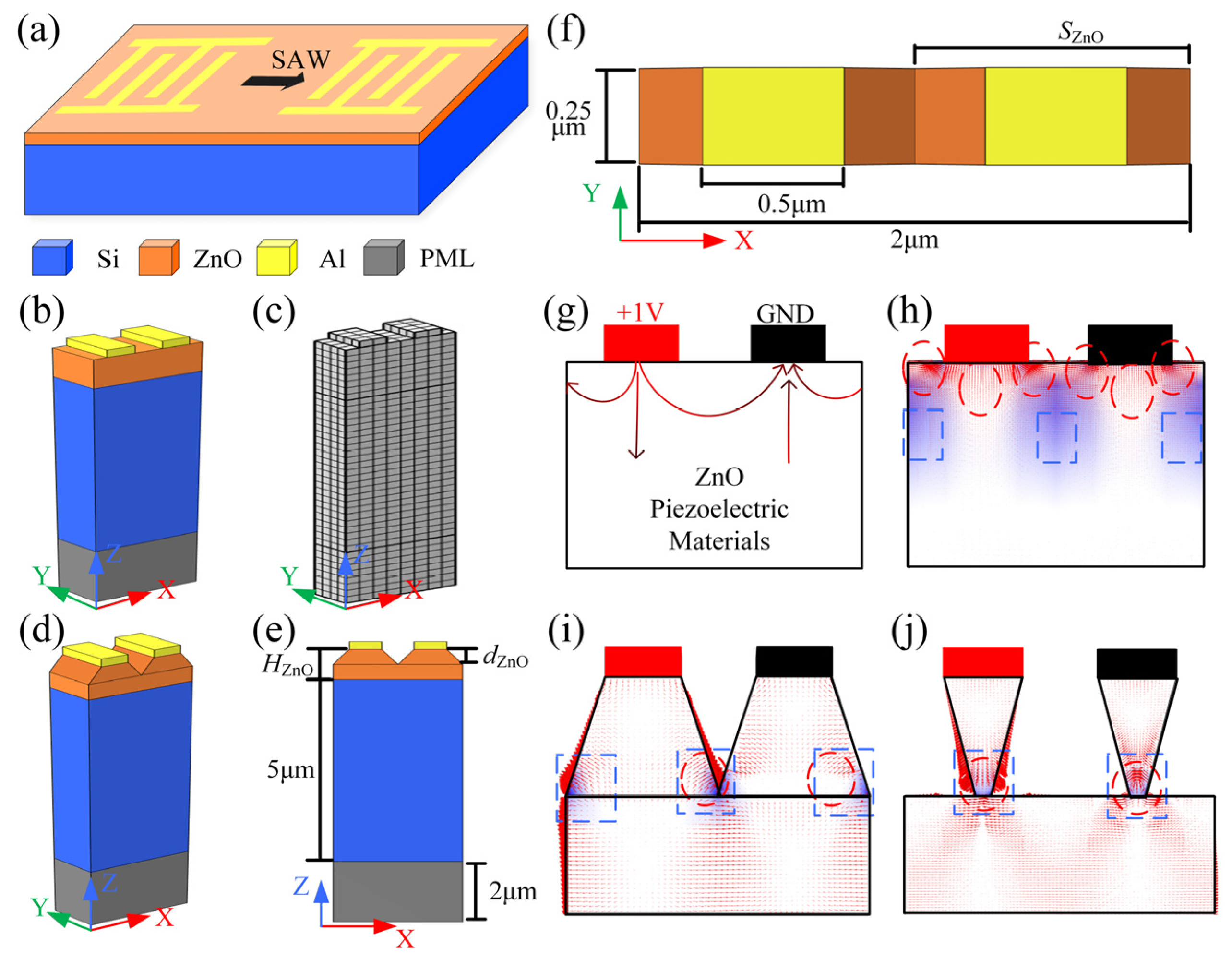
Based on the governing equations in (5), the simulation model of the SAW device was established by using the FEM. The structure primarily consists of four domains: the Si substrate, the ZnO piezoelectric layer, the Al interdigitated transducer (IDT) electrodes, and a Si perfectly matched layer (PML) to suppress boundary reflections, as shown in
Figure 1a. The IDT layer comprises two sets of periodically arranged comb-like metallic strip electrodes, which serve to excite and detect the surface acoustic waves. Leveraging the structural periodicity of the device, a single period was extracted to construct the conventional Al/ZnO/Si model, as shown in
Figure 1b [
29]. The simulation parameters are defined with the wavelength (
λ = 2 μm). The geometric dimensions are set as follows: Al electrodes (0.5 μm × 0.25 μm × 0.25 μm), Si substrate (2 μm × 0.25 μm × 8 μm), and the ZnO layer thickness of 1 μm. Corresponding periodic boundary conditions are applied. Although a finer mesh provides higher simulation accuracy, it also leads to an exponential increase in data volume and computational workload. Therefore, to achieve an optimal balance between accuracy and computational cost, a minimum mesh size of λ/8 was adopted in this study. The mesh partitioning diagram is shown in
Figure 1c. Similarly, while keeping the basic dimensional parameters and materials unchanged, the piezoelectric layer was etched to vary the etching ratio (
dZnO/
HZnO) and the bottom width (
SZnO). This yielded a simulation model of the Al/ZnO/Si structure with a trapezoidal profile, as shown in
Figure 1d.
Figure 1e,f illustrate the front and top views of the trapezoidally etched model, respectively.
The intensity and direction of the electric field are shown by the density of the field lines.
Figure 1g displays the actual electric field distribution under an applied IDT voltage, while
Figure 1h maps the mechanical energy (blue regions) and electric field (red lines) in the conventional structure. The simulations reveal a highly non-uniform electric field that is primarily confined to the top of the piezoelectric layer. Conversely, the mechanical energy fails to maintain this confinement, exhibiting significant acoustic leakage into the surrounding and underlying regions. This dissipated mechanical energy couples only weakly with the electric field, fundamentally hindering the enhancement of the electromechanical coupling coefficient.
To tackle this energy leakage, a trapezoidal etching strategy is applied to the piezoelectric layer to cut off the diffusion channels. This geometrically confines the mechanical energy strictly to the top region, allowing it to perfectly coincide with the densest electric field. As shown by the simulated distributions in
Figure 1i,j, the etched models maintain an electric field profile similar to the conventional one, yet successfully eliminate the massive mechanical diffusion. By tightly concentrating both fields at the top surface, this structure achieves deep spatial overlap and full electromechanical coupling, thereby maximizing the coupling coefficient.
To quantitatively analyze the trapezoidally etched structure, based on equations in (4), the
K2 is directly proportional to the Γ, which can be expressed as follows:
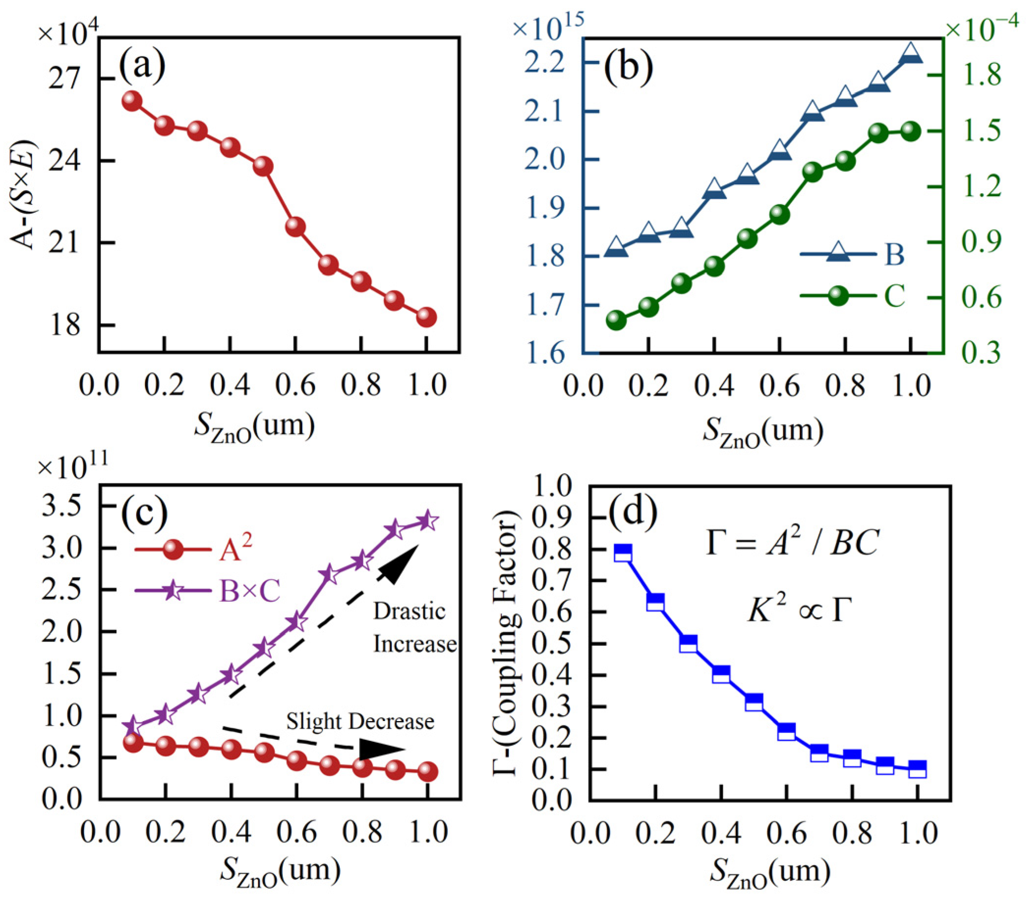
With the increase in
SZnO, the enlarged diffusion of mechanical energy weakens the electromechanical coupling effect, leading to a pronounced drop in the electromechanical energy density (A). In contrast, both the electrical energy density (B) and the mechanical energy density (C) exhibit a gradual increase, as shown in
Figure 2a,b.
Figure 2c,d plot the evolution of the mathematical term A
2/(B × C) and the overall coupling factor Γ. Notably, driven by the overwhelming magnitude of (B × C) relative to A
2, the coupling factor Γ strictly decreases as
SZnO widens, thereby dictating a proportional decay in the macroscopic coupling coefficient
K2.
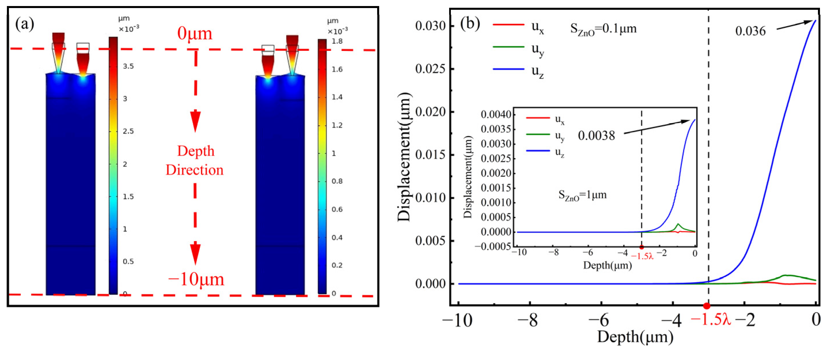
Figure 3 shows the FEM-simulated vibration mode and displacement profiles of the trapezoidally etched SAW device. As shown in
Figure 3a, the vibration amplitude decays with the depth of the piezoelectric layer. By defining the surface of the piezoelectric material as the reference zero point, the variation of the acoustic wave displacement along the depth is shown in
Figure 3b. The displacement components along the X-, Y-, and Z-direction are denoted as
ux,
uy, and
uz, respectively. It can be observed that the
ux and
uy components exhibit negligible displacement. The
uz component dominates the displacement and is primarily concentrated within a depth of approximately 3 μm (1.5
λ) from the surface. At depths exceeding 1.5
λ, the
uz displacement approaches zero. These results confirm that the acoustic waves generated by the etched SAW device exhibit characteristic Rayleigh wave behavior.
The wave velocity (
VP) of Rayleigh waves is calculated as follows [
30,
31]:
Similarly, the
K2 of Rayleigh waves is calculated as follows:
where
fr is the resonant frequency and
far is the anti-resonant frequency.
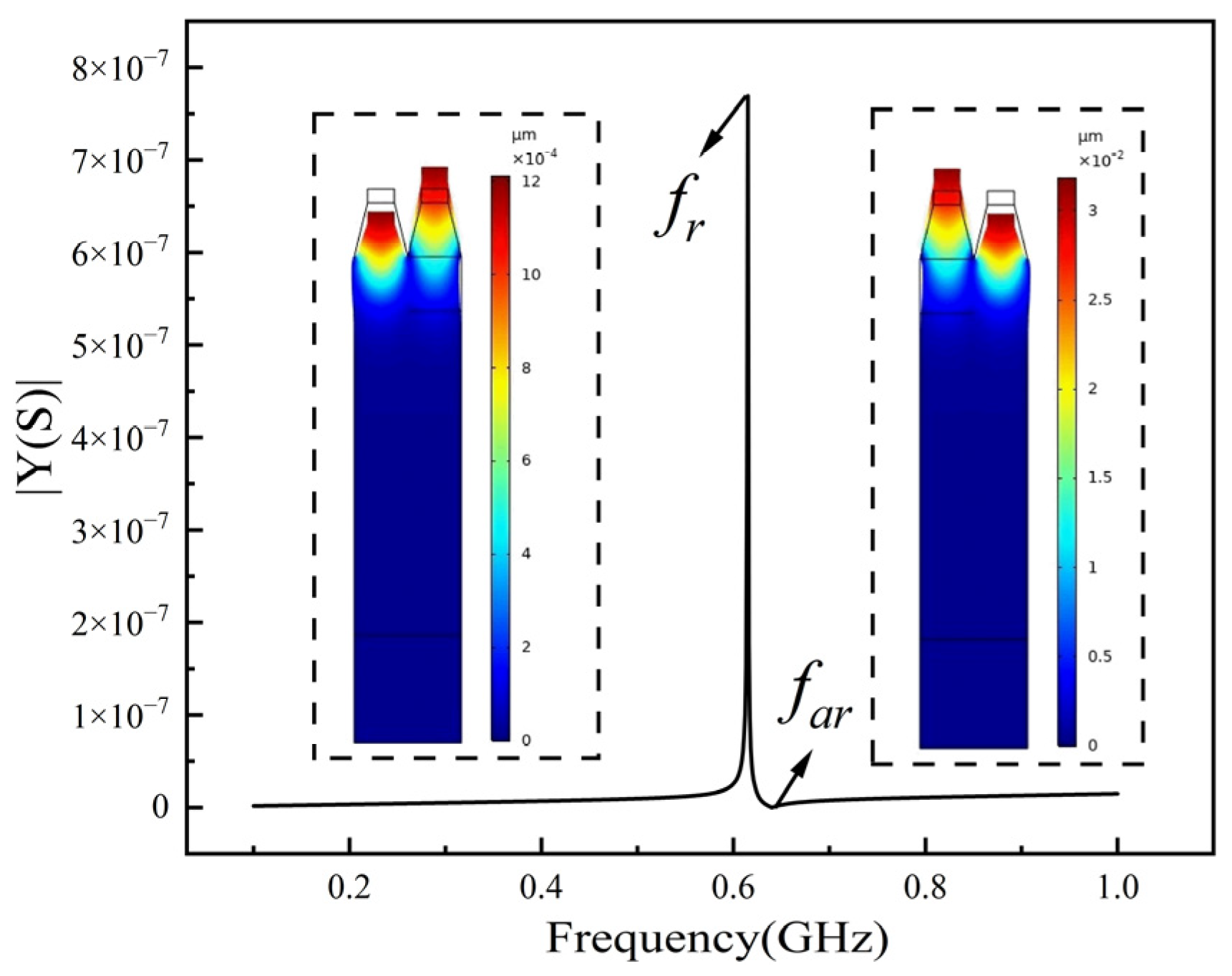
These parameters are obtained from the Rayleigh wave conductance curve, as shown in
Figure 4. On the admittance curve (
),
fr is the maximum value near the operating frequency, while
far is the minimum value.
The SAW generated by the trapezoidal etching of the Al/ZnO/Si structure modifies the conventional mechanism, in which piezoelectric materials directly excite SAW. This approach accounts for the coupling effect at the structural boundaries and incorporates process optimization of the structural dimensions through etching. Therefore, the influence of structural dimensions (HZnO, dZnO/HZnO, SZnO) on the electromechanical characteristics of SAW devices is investigated.
3. Results and Discussion
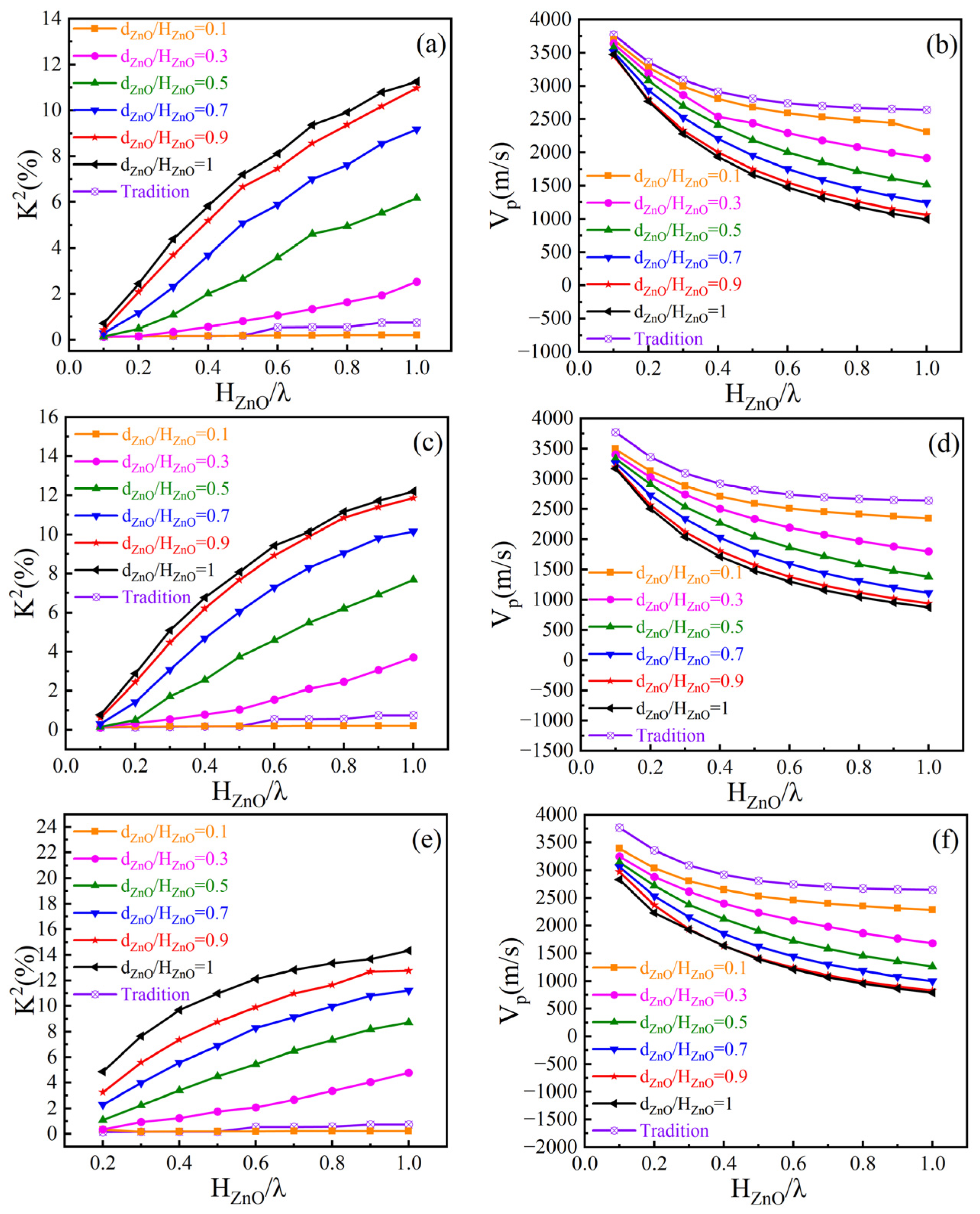
For trapezoidal etching, different etching shapes appear as SZnO decreases. Specifically, when 0.5 μm < SZnO ≤ 1 μm, the shape assumes a normal trapezoid; when SZnO = 0.5 μm, it takes the form of a rectangle; and when 0.1 μm ≤ SZnO < 0.5 μm, it transforms into an inverted trapezoid. This study investigates how the SAW device parameters, K2 and VP, vary with the normalized thickness (HZnO/λ) under different etching ratios for these three etching shapes.
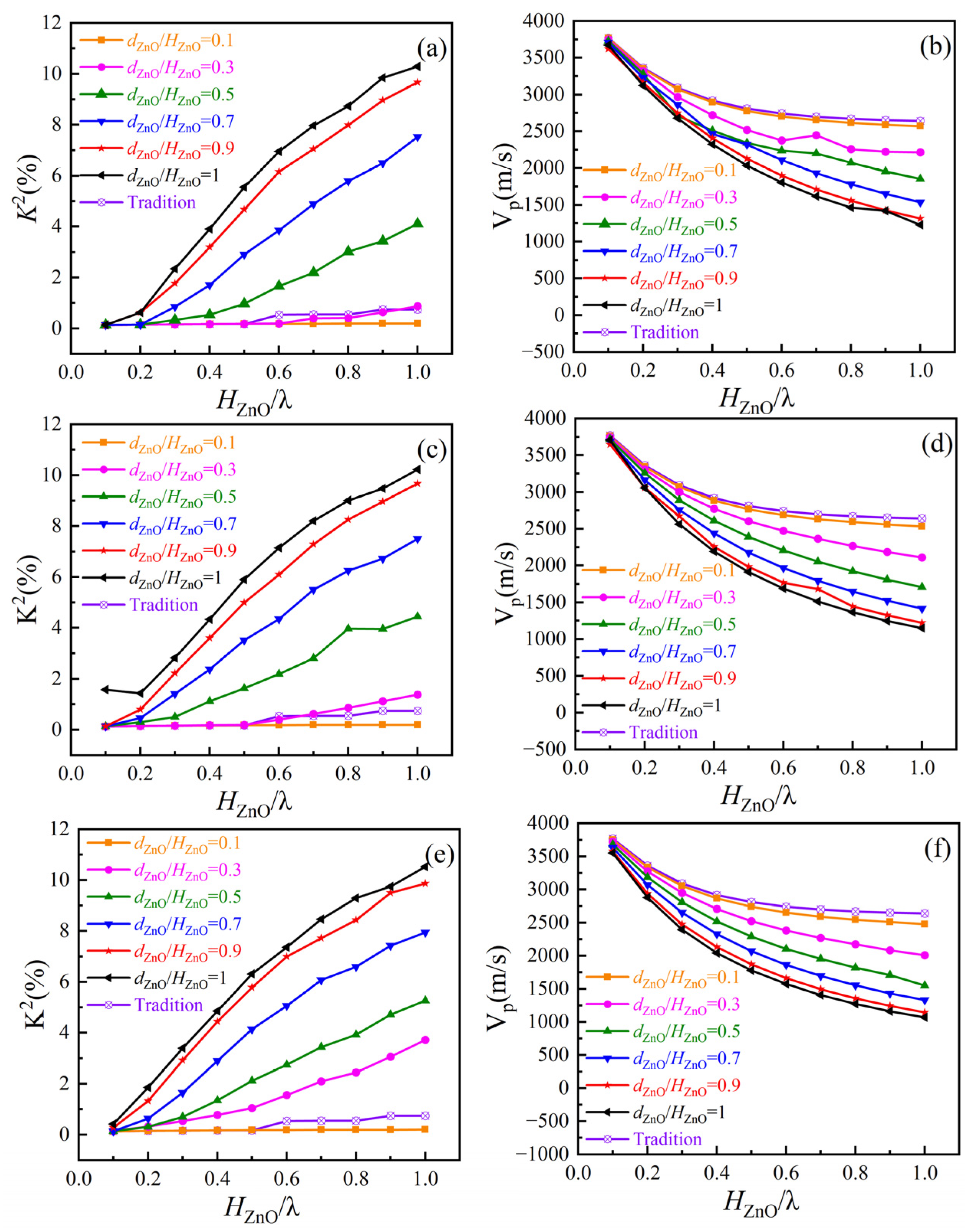
Figure 5 shows the variation of
K2 and
VP with normalized thickness for SAW devices under different etching ratios during normal trapezoidal etching. As shown in
Figure 5a,c,e, when
dZnO/
HZnO = 0.1–0.3, the increase in
K2 is relatively slow compared to the conventional structure, and
K2 can even be lower than that of the conventional structure, likely due to the negative effect of weak etching [
27]. The effect of etching becomes significant at
dZnO/
HZnO = 0.5, resulting in a notable increase in
K2 from 0.742%. When
dZnO/
HZnO = 1 and
HZnO/λ = 1, the
K2 of the SAW device reaches its maximum value. The energy of the Rayleigh wave is primarily concentrated within a depth of 1λ to 2λ from the surface. Once the piezoelectric material thickness reaches 1λ, it maximally prevents the leakage of Rayleigh wave energy into the non-piezoelectric substrate (Si). Simultaneously, the trapezoidal etching technique eliminates lateral energy dispersion channels, enabling optimal spatial coupling between mechanical energy and the electric field. This conclusion is consistent with [
19,
20,
30]. At this optimal point, the maximum
K2 is 10.522%, corresponding to an increase of 14.18 times relative to the conventional structure. Meanwhile,
VP reaches its minimum value of 995.1 m/s when
K2 is maximized, as shown in
Figure 5b,d,f.
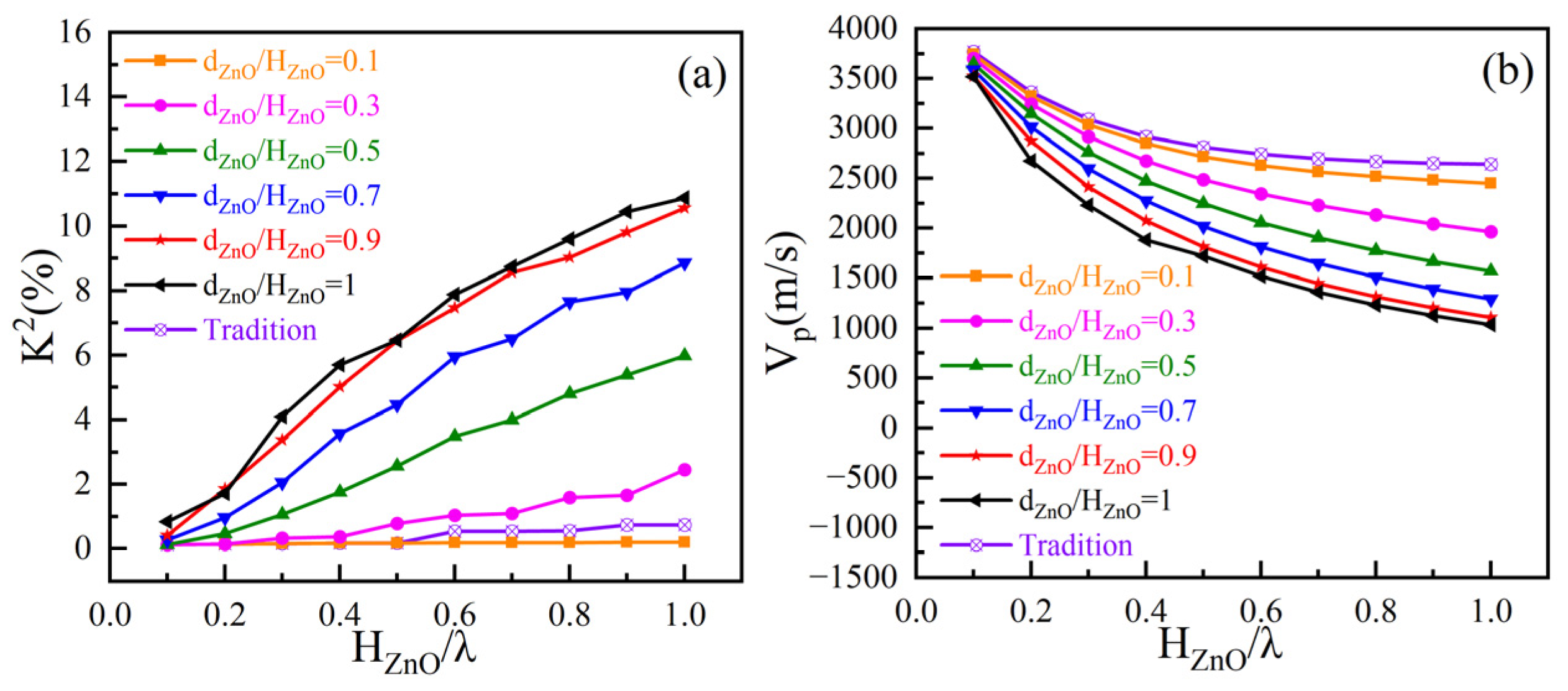
Figure 6 shows the simulated variation of
K2 and
VP with normalized thickness for SAW devices under different etching ratios during rectangular etching. The variation trends of
K2 and
VP for rectangular etching are similar to those of normal trapezoidal etching. Under the condition that
SZnO is fixed,
dZnO/
HZnO = 1, and
HZnO/λ = 1,
K2 reaches its maximum value of 10.875%, corresponding to an increase of 14.65 times relative to the conventional structure. At this point,
VP reaches its minimum value of 1034.4 m/s.
Similarly, as
SZnO decreases below 0.5 μm, the etching shape becomes an inverted trapezoid.
Figure 7 shows the variation of
K2 and
VP with normalized thickness for SAW devices under different etching ratios during inverted trapezoidal etching. As shown in
Figure 7a,c,e, when
SZnO = 0.1 μm,
dZnO/
HZnO = 1, and
HZnO/λ =1, the SAW device reaches its maximum
K2 of 14.34%, which corresponds to an increase of more than 19 times relative to the conventional structure. In summary, when
SZnO is fixed,
K2 increases with normalized thickness, and as the piezoelectric etching ratio increases,
K2 gradually approaches its maximum, while
VP decreases correspondingly.
To investigate the effect of
SZnO on
K2, the conditions
dZnO/
HZnO = 1 and
HZnO/λ =1 were selected. The simulated variation of
K2 and
VP with bottom width (
SZnO) for the SAW devices is shown in
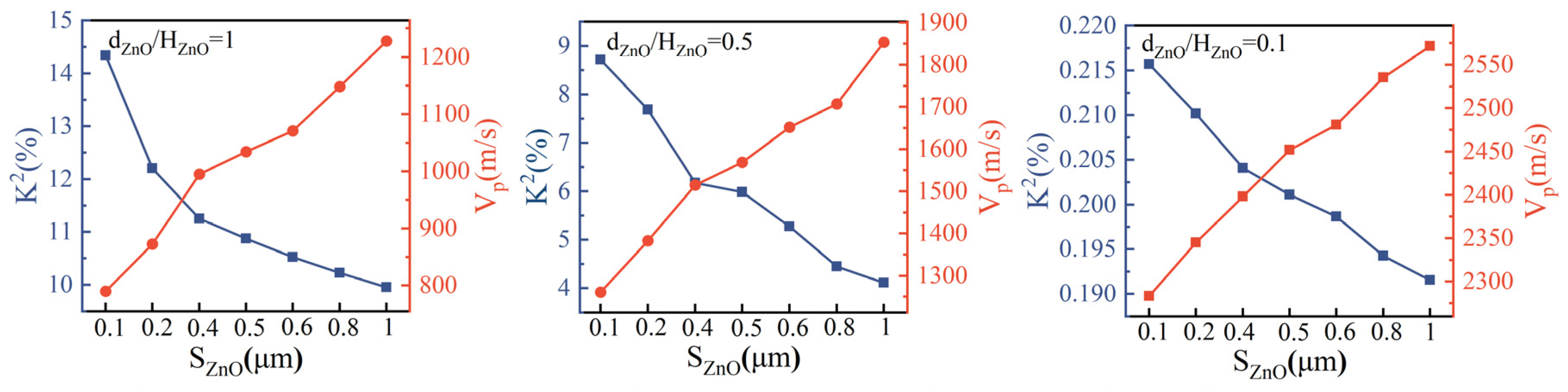
Figure 8. The results indicate that
K2 decreases with increasing
SZnO, with a maximum value of 14.34%. Conversely,
VP increases as
K2 decreases, exhibiting an opposite trend. To confirm the correctness of this behavior, additional simulations were conducted for
dZnO/
HZnO = 0.5 and
dZnO/
HZnO = 0.1. The results shown that the variation patterns of
K2 and
VP remained consistent across all conditions.
The preceding analysis reveals that the trapezoidal etched structure enables SAW devices to achieve a high
K2, thereby delivering significant performance improvements. However, the high performance of a SAW device is not solely reflected by the
K2 parameter alone. In practice, an analysis combining the FOM and
S21 is typically used as the standard for evaluating device performance. Therefore, while achieving a high
K2, it is essential to simultaneously investigate the FOM and
S21 [
29,
30].
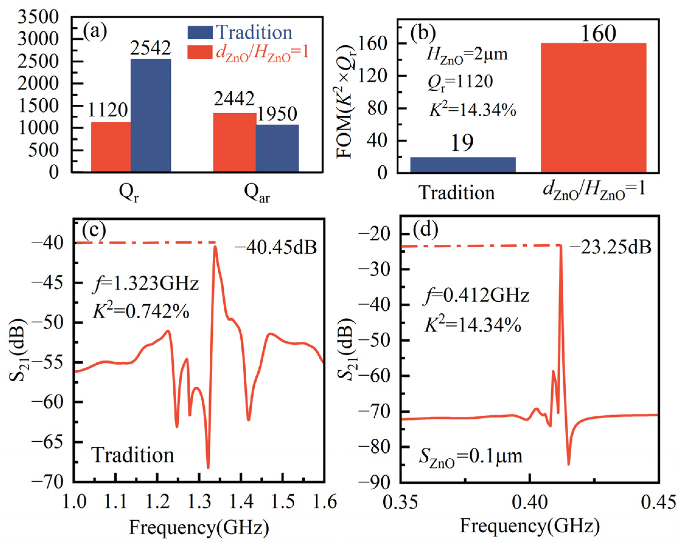
Figure 9 shows the variation of the FOM and
S21 for the SAW device at maximum
K2. To accurately evaluate the FOM of the SAW device (FOM =
K2 ×
Qr), the −3 dB bandwidth method was employed to extract the resonance quality factor (
Qr) and anti-resonance quality factor (
Qar) [
31], as depicted in
Figure 9a. It can be observed that
Qar increases significantly from 1950 to 2442, whereas
Qr decreases from 2542 to 1120. This reduction in
Qr is likely attributed to the increased electrical resistance caused by the narrowed piezoelectric layer after etching, as well as the emergence of spurious modes [
32,
33,
34,
35]. Nevertheless, compared to the conventional structure, the overall FOM of the etched SAW device is substantially enhanced, increasing from 19 to 160, as shown in
Figure 9b. Similarly, the
S21 is significantly improved following the trapezoidal etching; near the operating frequency,
S21 reaches an optimal value of −23.25 dB, representing a 42.5% reduction in absolute insertion loss compared to the conventional model, as shown in
Figure 9c,d. This improvement is primarily attributed to the strong spatial coupling between the mechanical energy and the electric field induced by the trapezoidal etching, which effectively mitigates energy leakage [
18].
4. Fabrication Trade-Offs
It is worth noting that although the performance of the SAW device is significantly enhanced when
K2 is maximized, the extreme profile (
SZnO = 0.1 μm) associated with this optimal inverted trapezoidal structure renders the device susceptible to severe microfabrication challenges and mechanical fracture risks. Among the three etching topologies investigated in this study (standard trapezoidal, rectangular, and inverted trapezoidal), the standard trapezoidal and rectangular geometries can effectively circumvent the aforementioned risks [
19,
21]. however, their enhancement of the
K2 remains limited. Therefore, despite the inherent fabrication risks of the inverted trapezoidal profile, systematically investigating the performance of SAW devices under less extreme inverted trapezoidal conditions (
SZnO = 0.2 μm and
SZnO = 0.4 μm) remains highly instructive for practical engineering applications. This optimal trade-off ensures that the proposed design possesses high engineering viability under current fabrication capabilities.
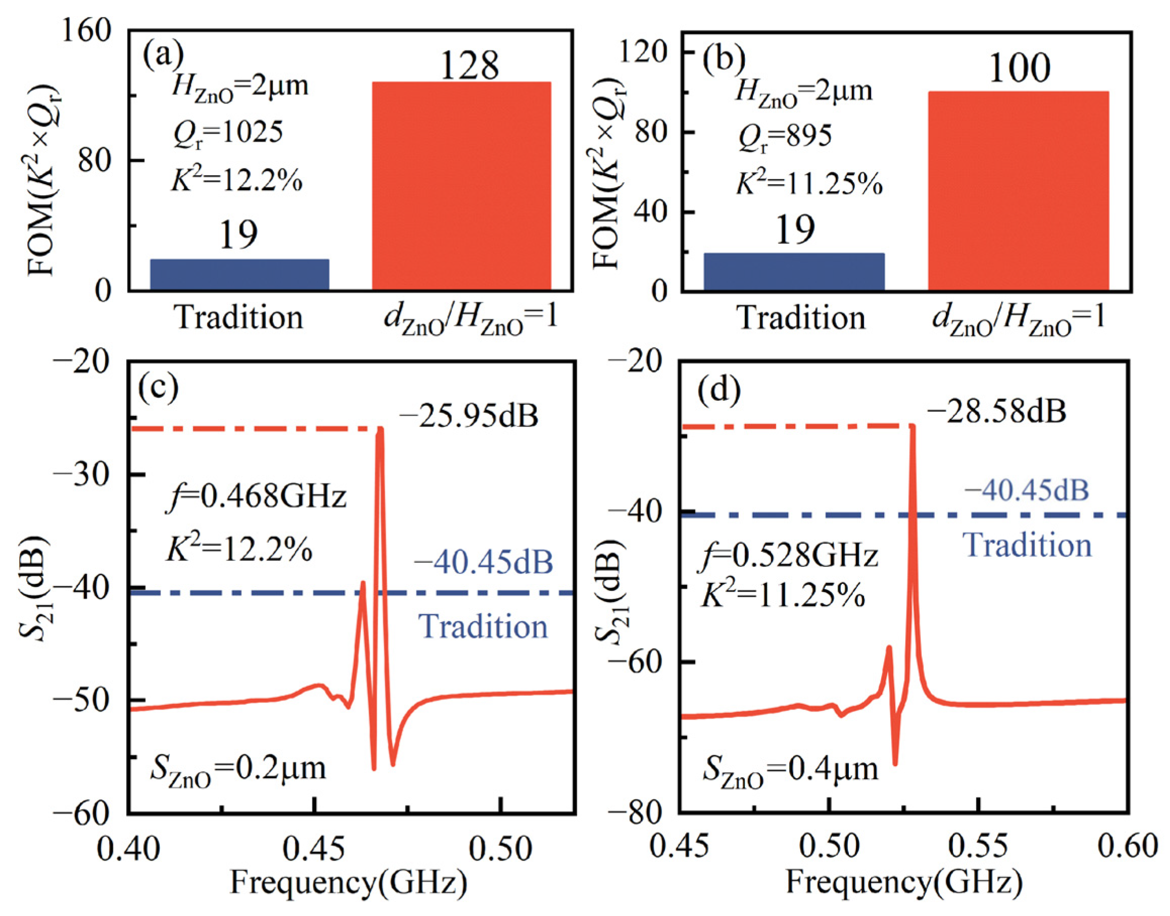
Figure 10 shows the variations in the figure of merit (FOM) and
S21 of the SAW devices under two inverted trapezoidal etching conditions (
SZnO = 0.2 μm and
SZnO = 0.4 μm). When
SZnO = 0.2 μm, the FOM increases to 128 and the
S21 improves to −25.95 dB, as depicted in
Figure 10a,c. It is noteworthy that the
SZnO = 0.4 μm configuration also significantly enhances device performance; although the improvement is less pronounced than that of the 0.2 µm case, the FOM still rises from 19 to 100, and the
S21 improves from −40.45 dB to −28.58 dB (representing a 29.34% reduction in
S21), as shown in
Figure 10b,d. These results indicate that while the optimal performance is achieved at
SZnO = 0.1 μm, the
SZnO = 0.2 μm and
SZnO = 0.4 μm profiles remain highly effective. Crucially, these configurations successfully balance manufacturing feasibility with the mitigation of mechanical fracture risks, offering a robust technical route for the development of high-performance SAW devices.