Abstract
This study examines the performance of a GaN HEMT with a 150 nm gate length, fabricated on silicon carbide, across various operational modes, including direct current (DC), radio frequency (RF), and small-signal parameters. The evaluation of DC, RF, and small-signal performance under diverse bias conditions remains a relatively unexplored area of study for this specific technology. The DC characteristics revealed relatively little Ids at zero gate and drain voltages, and the current grew as Vgs increased. Essential measurements include Idss at 109 mA and Idssm at 26 mA, while the peak gm was 62 mS. Because transconductance is sensitive to variations in Vgs and Vds, it shows “Vth roll-off,” where Vth decreases as Vds increases. The transfer characteristics corroborated this trend, illustrating the impact of drain-induced barrier lowering (DIBL) on threshold voltage (Vth) values, which spanned from −5.06 V to −5.71 V across varying drain-source voltages (Vds). The equivalent-circuit technique revealed substantial non-linear behaviors in capacitances such as Cgs and Cgd concerning Vgs and Vds, while also identifying extrinsic factors including parasitic capacitances and resistances. Series resistances (Rgs and Rgd) decreased as Vgs increased, thereby enhancing device conductivity. As Vgs approached neutrality, particularly at elevated Vds levels, the intrinsic transconductance (gmo) and time constants (τgm, τgs, and τgd) exhibited enhanced performance. ft and fmax, which are essential for high-frequency applications, rose with decreasing Vgs and increasing Vds. When Vgs approached −3 V, the S21 and Y21 readings demonstrated improved signal transmission, with peak S21 values of approximately 11.2 dB. The stability factor (K), which increased with Vds, highlighted the device’s operational limits. The robust correlation between simulation and experimental data validated the equivalent-circuit model, which is essential for enhancing design and creating RF circuits. Further examination of bias conditions would enhance understanding of the device’s performance.
1. Introduction
The beneficial properties of GaN HEMTs have made them a focal point in the semiconductor industry. Due to their high breakdown voltage, high electron mobility, and high thermal conductivity, they are suitable for high-power and high-frequency applications [1,2,3,4]. Compared to conventional silicon and GaAs devices, GaN HEMTs that utilize silicon carbide (SiC) substrates offer even greater benefits. SiC’s exceptional thermal conductivity enhances the efficiency and power density of various systems, including radar systems and RF amplifiers, by effectively dissipating heat during high-power operation [5,6,7,8,9,10]. Despite numerous studies examining the DC and RF performance characteristics of GaN HEMTs [11,12,13,14,15,16,17,18,19,20,21,22,23,24], there is limited information available regarding their behavior under varying bias conditions, especially concerning small-signal and multi-bias performance [25,26,27,28,29,30]. To design and analyze GaN RF circuits, it is essential to investigate how multi-bias conditions influence crucial parameters, including transconductance (gm), output resistance (Rds), and intrinsic capacitances. Existing literature has primarily focused on basic DC characteristics under static bias conditions, with earlier work addressing only the influence of bias on switching ability and efficiency. Prior research has focused on the effects of passive and active parasitics, leaving the dynamic impact of bias on RF and small-signal parameters less studied. For example, some research has examined the effects of parasitic components on frequency response and stability [31,32,33], while other research has focused on bias-related noise performance [14,34,35]. However, there has not been a thorough examination of DC, RF, and small-signal characteristics under various bias conditions. The objective of this research is to investigate the behavior of a GaN HEMT 150 with a 150 nm gate length, built on a SiC substrate, and to highlight the impact of bias conditions on equivalent circuit components and high-frequency performance.
Key DC results that highlight the device’s performance capabilities include Idss, which was measured at 109 mA, and Idssm, which was measured at 26 mA. The device’s sensitivity to these biasing parameters is further illustrated by the transconductance (gm), which attained 62 mS at Vgs = −4.8 and Vds = 10 V. Due to short-channel effects, such as DIBL, the threshold voltage (Vth) decreased as Vds increased, with values ranging from −5.06 V to −5.71 V. At higher Vds, the dark current (Idso) increased exponentially, indicating an increase in carrier generation. An equivalent circuit analysis shows how extrinsic elements, such as parasitic resistances and capacitances, affect performance. Biasing ranged from Vgs = −6.0 V to −3.0 V and from Vds = 3 V to 15 V, with a focus on frequencies between 45 MHz and 50 GHz. The extraction process for device parameters starts by identifying extrinsic components to determine intrinsic parameters. Cgs increased with both Vds and Vgs, while Cgd decreased. Simultaneously, Cds rose as Vgs neared pinch-off. Owing to non-quasi-static phenomena, the series resistances Rgs and Rgd exhibited charging delays, whereas Rds increased with Vds, necessitating a balance for optimal design. At Vds = 11 V and Vgs = −4.8 V, the intrinsic transconductance gmo reached a maximum of 71 mS. It escalates with Vgs. Transistor inertia at elevated frequencies is indicated by intrinsic gmo and time constants (τgm, τgs, and τgd), with gmo reaching its maximum at reduced Vgs as Vds increased. Increased Vds and decreased negative Vgs yielded enhanced frequency performance metrics, with fT ranging from 1.18 × 10⁸ Hz to 5.16 × 10¹⁰ Hz and fmax from 5.23 × 10⁸ Hz to 9.96 × 10¹⁰ Hz. The S21 parameter peaked at 11.2 dB with Vgs = −4.8 V and Vds between 11 and 15 V. Furthermore, the stability factor K increased with higher Vds and lower Vg, reaching a maximum of approximately 1.3, indicating unconditional stability. This work utilises small-signal parameters derived from measured S-parameters in ADS software 2022 to compare simulations with measurements through an equivalent circuit model.
This research aims to investigate how biasing influences GaN HEMTs, particularly their small-signal operation and RF performance. It proposes a systematic method for evaluating circuit components under varying bias conditions, which is crucial for optimizing GaN HEMTs for high-power and high-frequency applications, thereby advancing semiconductor technology.
2. Fabrication and Measurements
This study aims to investigate a HEMT based on an AlGaN/GaN heterostructure [36] grown by metalorganic vapor-phase epitaxy (MOVPE) on a 400-µm-thick silicon carbide substrate, as in Figure 1. A GaN buffer layer was incorporated into the design to achieve a 2-DEG at the AlGaN-GaN junction, which relies on the charge induced by polarization between the AlGaN and GaN layers, thereby providing a good number of electrons without the need for impurity doping. The device utilized a 20 nm Al0.253Ga0.747N barrier and a 1.5 µm GaN buffer epitaxial layer to achieve a good lattice match with the substrate (SiC). This was succeeded by a GaN channel layer and a very thin 5 nm AlGaN spacer layer, which also enables high-speed electron motion and facilitates the modulation of charge density through control of the gate bias voltage applied. To obtain low-resistance ohmic contact at the source and drain regions, a thin 5 nm cap layer of GaN was deposited. Important parameters recorded include the sheet resistance (RSH) of 324 Ω/□ from Hall measurements, and TLM showed the contact resistance (Rt) to be 0.36 Ω·mm. In Hall measurements, the charge density (NS) was greater than 1.3 × 1013 cm−2, and the most significant electron mobility was higher than 1400 cm2/V·s. The gate configuration comprised four 50 µm fingers, resulting in an overall gate width of 200 µm and a gate length of 0.15 µm. Ohmic contacts of Ti/Al/Ni/Au were created by thermally annealing at 900 °C. The mushroom-shaped Schottky gate consisted of a Pt/Ti/Pt/Au stack, which helps reduce the gate capacitance and consequently enhances the control of transconductance, while decreasing leakage and noise. The device was encapsulated with a 240 nm thick Si3N4 layer, deposited by PECVD at 340 °C, to further enhance efficiency and reliability. The transistors were manufactured using the UMS GH15 process. They were created through Molecular Beam Epitaxy (MBE) at IEMN in the University of Lille, France.
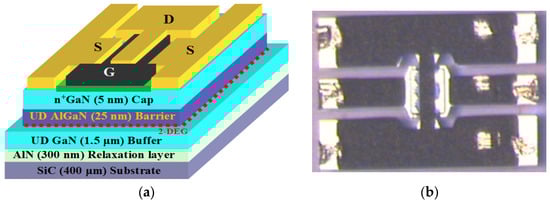
Figure 1.
(a) Cross-section view of AlGaN/GaN/SiC HEMT structure (not to scale); (b) optical micrographs [36].
Four main steps comprise the device characterization process as illustrated in Figure 2: (1) S-parameter acquisition, (2) cold pinch-off technique, (3) de-embedding, and (4) ADS simulation flow. First, an HP8510C Vector Network Analyzer (VNA), with the aid of an HP4142B DC source, supplied the required current, connected via Ground-Signal-Ground (GSG) radio frequency probes that spanned 45 MHz to 50 GHz, to measure S-parameters. Multiple biasing conditions (Vgs from −6 V to –3 V and Vds from 3 V to 15 V) were used for the measurements, and IC-CAP software 2022 was employed to automate data acquisition and ensure accuracy. In the second step, extrinsic parasitic components like inductances (Lg, Ld, Ls), resistances (Rg, Rs, Rd), and pad capacitances (Cpg, Cpd) could be accurately extracted by suppressing intrinsic device activity using the cold pinch-off technique with Vgs = −10 V and Vds = 0 V. Third, by gradually modifying and eliminating capacitance values (Cpg and Cpd), a de-embedding procedure was carried out to eradicate parasitic effects, especially the PDRZ effect, until the frequency-dependent anomalies in Re (Zij) were removed. Inductive and resistive parameters were also extracted using OFF-state bias data (Vgs = 0 V, Vds = 0 V). A comprehensive small-signal equivalent circuit model was then constructed by importing the cleaned and bias-dependent S-parameter data into the Advanced Design System (ADS). Both extrinsic and intrinsic components (gm, Cgs, Cgd, Cds, Rgs, Rgd, and Rds) were included in this model, which was validated through simulations under all tested frequencies and bias conditions.
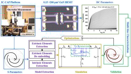
Figure 2.
Diagram depicting the methodology for quantifying and assessing 150 nm GaN HEMT.
3. Results and Analysis
The operation of HEMTs can be described across different voltage regions. In the sub-threshold region, when Vgs is less than Vth, the current increases exponentially with Vgs, but is small enough, making it suitable for ultra-low-power device applications. When the dependence of Vgs surpasses Vth and Vds is adequately elevated, the square law region fluctuates, yielding a current that is roughly equivalent to Vgs squared. This region is optimal for amplifiers due to the advantageous correlation between Vgs and current, making it a preferred choice in analog circuit designs. In this instance, the transconductance (gm) increases with current. In contrast, elevated Vgs values lead to the saturation of carrier velocity within the velocity saturation region, maintaining constant transconductance and diminishing the increase in current, thereby affecting performance. When selecting Vgs = −3.0 V to −7.0 V and Vds = 3 V to 15 V, it is recommended that Vgs be maintained above the threshold level for maximum amplification, and Vgs should not enter the velocity saturation region. Regarding the square-law region, its emphasis enables most of the HEMT’s characteristics to be effectively exploited, which is why it is suitable for use in high-performance analog circuits.
3.1. DC Behavior with Biasing
Figure 3a illustrates the DC attributes of a GaN HEMT. Even with Vds and Vgs equal to zero, there is practically no drain current (Ids), which is usually less than the reverse leakage current [16]. As the gate voltage increases, the current through the drain also increases. The data can be divided into two main regions: the triode region, characterized by a linear increase in Ids with rising Vds, and the saturation region, where Ids becomes limited or saturated once Vds reaches a specific threshold due to channel constriction at the drain side [37]. From the I–V graph, two key metrics emerge: Idss, the drain current when the transistor was saturated at Vgs = −3.0 V, measured at 109 mA, and Idssm, the maximum drain-source current at peak transconductance, recorded at 26 mA. Figure 3b,c show the transconductance (gm) and transfer characteristics (gm versus Vgs and Ids versus Vgs). The maximum transconductance achieved was 62 mS at Vgs = −4.8 V and Vds = 10 V, resulting in a ratio of 4.23 between Idss and Idssm, which indicates optimal small-signal gain [38]. The maximum transconductance values were determined at different combinations of Vgs and Vds. The measurements revealed a transconductance of 46.23 mS with Vgs at −4.6 V and Vds at 3 V. A transconductance of 54.48 mS was observed at a Vgs of −4.6 V and a Vds of 6 V. The peak transconductance of 59.62 mS was attained at a Vgs of −4.7 V and a Vds of 9 V. A value of 57 mS was recorded at Vgs of −4.8 V and Vds of 12 V. A transconductance of 56.8 mS was observed at a Vgs of −4.9 V and a Vds of 15 V. These values underscore the sensitivity of transconductance to variations in both Vgs and Vds within the designated ranges. As Vds increased from 3 V to 15 V, the peak transconductance (gm) changed from −4.6 V to −4.9 V. This is because threshold voltage (Vth) varies with Vds, a phenomenon known as “Vth roll-off” [39]. The roll-off has a significant impact on how well the device performs. As Vds increases, Vth decreases, which means that Vgs must be adjusted to maintain the desired conduction levels. This behavior improves transconductance and overall efficiency between −4.6 V and −4.9 V. These differences demonstrate the importance of carefully managing circuit design to ensure that biasing, gain, and overall reliability are stable. Figure 3c shows that the threshold voltage (Vth) values had a consistent trend in the transfer characteristics (Ids vs. Vgs). The Vth values were −5.06 V at Vds = 3 V, −5.19 V at Vds = 5 V, −5.32 V at Vds = 7 V, −5.43 V at Vds = 9 V, −5.50 V at Vds = 11 V, −5.59 V at Vds = 13 V, and −5.71 V at Vds = 15 V. The decrease in Vth as Vds rises suggests that higher drain-source voltages lower the threshold voltage, possibly because of short-channel effects like drain-induced barrier lowering (DIBL) [40]. This observation is essential for understanding device performance in low-voltage applications. Vds and effective channel length influence Vth in short-channel HEMTs but remain unaffected by channel width [41]. The semi-log transfer curve in Figure 3d shows the drain-to-source dark current (Idso) measurements, indicating a notable variation in current levels as Vds increased. The dark currents observed were 1.66 pA, 0.27 pA, 8.85 nA, 4.42 nA, 0.78 nA, 2.38 µA, and 5.19 µA for Vds values of 3 V, 5 V, 7 V, 9 V, 11 V, 13 V, and 15 V, respectively. This pattern suggests an exponential growth in dark current with increasing Vds, possibly indicating enhanced carrier generation or reduced barrier potential at higher voltages [42,43].
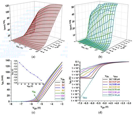
Figure 3.
(a) DC characteristics, (b) transconductance characteristics, (c) transfer characteristics, and (d) semi-logarithmic transfer characteristics.
3.2. Equivalent Circuit Parameters with Biasing
The equivalent-circuit approach [44], outlined in Figure 4, is employed to evaluate the S-parameters of the device. The equivalent-circuit parameters (ECPs) were determined using the “cold” pinch-off technique, a method that has been successfully used in GaN technology for many years. Our analysis focused on the extrinsic parameters of the semiconductor device, particularly the parasitic capacitances (Cpg and Cpd), parasitic inductances (Lg, Ld, and Ls), and terminal resistances (Rs, Rg, and Rd), among other factors. When the device was under pinch-off bias conditions (Vds = 0, Vgs = −10 V), it was observed that the parasitic capacitances primarily affected the imaginary part of the Y parameters. We also examined the frequency dependence of these capacitances. Figure 5 depicts the behavior of Re (Zij) for the GaN device as a function of frequency under “unbiased” conditions. The device exhibited the PDRZ effect [45], with Re (Zij) starting to rise significantly for the GaN around 36 GHz. The values of Re (Zij) continued to rise with increasing frequency after this onset frequency. The PDRZ effect could be removed from the de-embedded data by deducting the appropriate values of Cpg and Cpd from the measured data and gradually increasing them from zero until the effect was eliminated. To extract the extrinsic inductances, we used hypothetical Z parameters at OFF bias conditions (Vds = 0, Vgs = 0 V) across a specific frequency range. The results showed that inductance Lg was significantly more prominent in devices with longer gate lengths. Additionally, it was found that the terminal resistances were heightened due to the influence of the contact metal in the semiconductor. Amongst the three terminal resistances, Rg was the smallest, reflecting the effects of metallization in this device. Table 1 presents all the extrinsic parameters of the device.
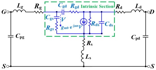
Figure 4.
The equivalent circuit model for the investigated GaN HEMT.
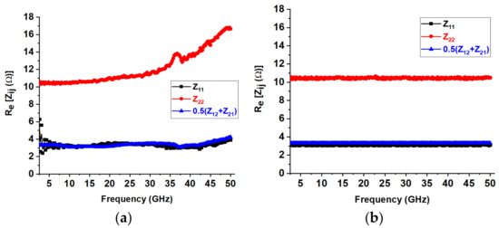
Figure 5.
Re (Zij) against frequency under zero bias condition: (a) before and (b) after de-embedding of the extrinsic capacitances.

Table 1.
Extrinsic parameter values of the GaN HEMT.
The initial phase of the extraction process is dedicated to identifying the extrinsic parameters. The intrinsic parameters can be established once these parameters are minimized. The applied bias ranged from Vgs = −6.0 V to −3.0 V and Vds = 3 V to 15 V, with intrinsic parameters being extracted between 45 MHz and 50 GHz. Figure 6a shows that the gate-source capacitance, Cgs, went up when both Vds and Vgs went up. Cgs stands for the capacitance between the gate electrode and the channel. It shows very non-linear behaviour. It includes both depletion and inversion charges, which are essential for determining the extrinsic cut-off frequency. Cgs decreases as Vgs decreases owing to the widening of the gate-source depletion region at higher negative voltages [46]. Furthermore, Cgd represents the feedback capacitance between the gate and drain, as shown in Figure 6b. Remarkably, this capacitance decreased at higher Vds, contrasting with the lower Cgd values observed at high negative Vgs across varying Vds. As Vgs increased at a constant Vds, Cgd gradually rose. The subsequent capacitance analyzed is the drain-source capacitance, Cds, depicted in Figure 6c with Vgs and Vds. As Vgs rose from −6 V to −3 V, the Cds values demonstrated a significant increase, especially at lower Vds values. The capacitance substantially rose as Vgs transitioned from −6 V to −5.2 V, indicating a substantial effect of gate voltage on capacitance. The effect of changing Vds is clear, especially in the middle range of Vgs. On the other hand, changing Cds values has a bigger effect when Vgs changes. The series resistances, Rgs and Rgd, are derived from the real components of Y11 and Y12, respectively. The charging delay resulting from non-quasi-static effects is depicted by the distributed channel resistances Rgs and Rgd [47] in Figure 7a,b. As Vgs went from −6 V to −3 V, the Rgs resistance values showed a clear downward trend. The resistance was relatively high when Vgs was low, such as around −6 V. However, it dropped significantly as Vgs increased, especially between −5.4 V and −4.8 V. This behavior indicates that within this range, elevated gate voltages result in lower resistance. The overall trend suggests a more pronounced decline with increasing Vgs, even though variations in Vds also affect the resistance values. As Vgs rose from −6 V to −3 V, the Rgd values typically exhibited a declining trend. At reduced Vgs values, especially at −6 V, the resistance was comparatively elevated, reaching its maximum at increased Vds levels. As Vgs rose, particularly between −5.4 V and −4.8 V, Rgd declined considerably, indicating that elevated gate voltages result in reduced resistance. Although changes in Vds affected Rgs, the main trend indicates that Vgs had the most significant impact on resistance characteristics. The “anomalous dip” in S-parameters is more pronounced in devices connected in series to gate-drain capacitance with higher effective gate-drain channel resistance (Rgd).
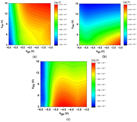
Figure 6.
Variation in intrinsic capacitances plotted at different Vds and Vgs for the AlGaN/GaN/SiC HEMT: (a) Cgs, (b) Cgd, and (c) Cds.
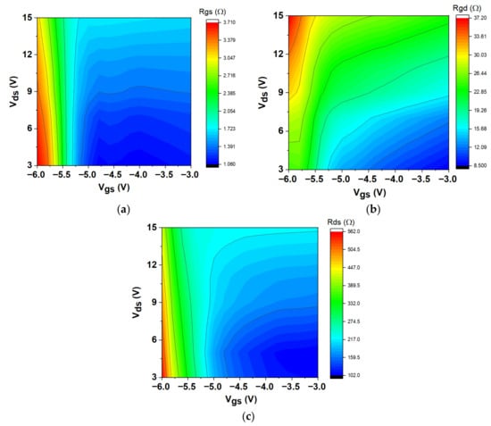
Figure 7.
Variation in intrinsic resistances plotted at different Vds and Vgs: (a) Rgs, (b) Rgd, and (c) Rds.
As the Vgs rose from −6 V to −3 V, the Rds values usually showed a decreasing trend, as shown in Figure 7c. Rds was relatively high at lower Vgs values (roughly −6 V), indicating that the device was less conductive. Rds dramatically decreased as Vgs increased, particularly between −5.4 V and −4.8 V, suggesting that the device has better conductivity at higher gate voltages. The overall pattern indicates that higher Vgs values result in lower Rds, underscoring the influence of gate control on the device’s conductivity. In addition, the Rds values vary with Vds.
Figure 8 illustrates the intrinsic transconductance (gmo) alongside three intrinsic time constants (τgm, τgs, and τgd). The time constants arise from the transistor’s inherent delay in reacting to rapid signal variations and represent the intrinsic non-quasi-static (NQS) effects that become increasingly pronounced at elevated frequencies. As Vgs transitioned from −6 V to −3 V, gmo typically rose across all Vds levels, signifying improved conductivity and the creation of channels within the transistor. The gmo values were noticeably low at Vgs = −6 V, suggesting that there was insufficient gate voltage for strong channel formation. On the other hand, gmo attained significantly greater values at Vgs = −3 V, peaking at roughly 0.071 mS at Vds = 11 V, suggesting adequate amplification. The data indicate that as Vds increases, gmo tends to stabilize, signifying that the transistor entered the saturation region where further increases in Vds have a decreasing impact on gmo. The time delay τgm in a transistor circuit indicates that as Vgs becomes less negative, τgm typically decreases. This means that charge carriers can move around more easily and respond faster. The time delay increased when Vgs was lower, such as when it was close to −6 V, because the conductivity was insufficient. On the other hand, values close to −3 V showed minimal delay, which is perfect for quick switching.
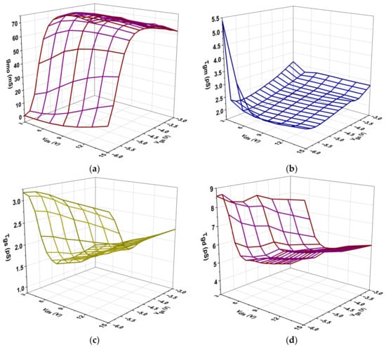
Figure 8.
Variation in intrinsic parameters plotted at different Vds and Vgs for the AlGaN/GaN/SiC HEMT: (a) gmo, (b) τgmo, (c) τgs, and (d) τgd.
Furthermore, increasing the Vds can improve performance, although delays may stabilize at elevated levels due to saturation effects. This relationship is crucial for designing high-speed circuits. The intrinsic time delay values, τgs, ranged from approximately 3.18 × 10⁻¹² s at Vgs = −6 V and Vds = 3 V to about 1.29 × 10⁻¹² s as Vgs approached −3 V with increasing Vds. This pattern implies that lower τgs is linked to higher Vgs, suggesting a quicker transistor response, particularly at higher Vds levels. The intrinsic time delay values τgd ranged from approximately 8.59 × 10⁻¹² s at Vgs= − 6 V and Vds = 3 V to about 3.47 × 10⁻¹² s at Vgs = −3 V and Vds = 3 V. A quicker gate-drain response was indicated by decreasing τgd values as the Vgs became less negative. According to this pattern, improved transistor switching speeds—which are essential for high-frequency applications—are a result of higher Vgs.
Even in the presence of parasitic effects, Figure 9 demonstrates that the measured h21 and MAG exhibited ideal behaviour, declining with frequency at a rate of −20 dB/decade. The ft and fmax obtained from the data are displayed in the inset images in Figure 9c,d, which show an inversion at various Vds values. When Vds was higher and Vgs was less negative, the cutoff frequency (Figure 9a) typically increased, indicating improved device performance. The range of values was approximately 1.18 × 10⁸ Hz to 5.16 × 10¹⁰ Hz. Better device performance under these bias conditions was indicated by the fmax (Figure 9b), which normally increases with increasing Vds and decreasing negative Vgs. The range of the fmax values was approximately 5.23 × 10⁸ Hz to 9.96 × 10¹⁰ Hz. The transistor’s suitability for high-frequency applications, such as RF amplifiers and high-speed switching, is demonstrated by both ft and fmax [48].
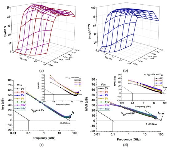
Figure 9.
Variation in cut-off and maximum frequencies: (a) ft, (b) fmax, (c) h21, (d) MAG.
In Figure 10, the impact of biasing on the real part of Y21, the magnitude of S21, and the stability factor K, is illustrated. It is essential to note that the low-frequency values of both Y21 and S21 are specifically correlated with the intrinsic transconductance gmo, as depicted below [49]:
where Z0 equals 50 ohms, which is generally much smaller than 1/Y22.
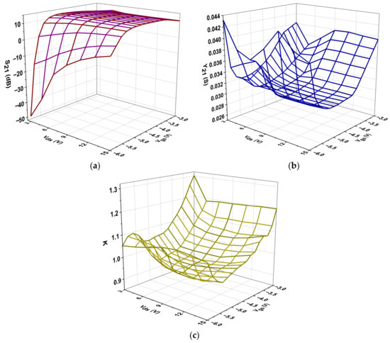
Figure 10.
Variation in the intrinsic parameters: (a) S21, (b) Y21, and (c) K.
The S21 parameter indicates that the values were highly negative at lower Vgs, such as −6 V, but increased significantly as Vgs approached −3.0 V, reflecting improved signal transmission. The highest S21 values, approximately 11.2 dB, occurred when Vgs = −3.2 V and Vds ranged from 11 to 15 V. Additionally, beyond a certain point, higher Vds values resulted in smaller gains, indicating the transistor’s limitations. As the drain-source voltage rose, the Y21 values typically increased with higher Vds across the various Vgs values, indicating improved signal transmission. The Y21 values tended to rise as Vgs became less negative (going from −6 V to −3 V), suggesting improved conductivity and transmission properties of the transistor. The values, which fell between roughly 0.032 and 0.043, indicate that the transistor exhibits good signal amplification capabilities within the tested voltage range. As Vds rose, the stability factor K usually increased as well. This was especially noticeable at Vgs = −3 V, where K peaked at about 1.30. Conversely, lower Vgs values exhibited a decreasing trend in K for most Vds levels, particularly at Vgs = −6 V, where K initially started at around 1.05 but increased slightly at higher Vds values.
The equivalent-circuit model’s precision in depicting the device’s performance under these conditions is corroborated by the robust correlation between simulations and experimental data (Figure 11). Table 2 shows the coefficient of determination (R2) and root mean square error (RMSE) values for each bias setting. This was to verify that the simulated and experimental results are in agreement. The model’s accuracy was validated by the low RMSE and high R2 values; the former indicates the magnitude of error between the simulated and observed S21 values, while the latter demonstrates the robustness of the linear correlation. This validation is essential for assessing practical performance, optimizing design, and advancing complex RF integrated circuit designs.
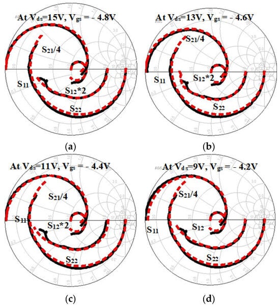
Figure 11.
Verification of experimental (black) and modeled (red) data: (a) at Vds = 15 V, Vgs = −4.8 V, (b) at Vds = 13 V, Vgs = −4.6 V, (c) at Vds = 11 V, Vgs = −4.4 V, and (d) at Vds = 9 V, Vgs = −4.2 V.
Table 2.
Quantitative comparison between simulated and experimental data (Figure 11).
The data in Table 3 illustrate the performance of the GaN HEMT at varying Vds with a constant Vgs of −4.8 V. The Ids consistently rose from 21.81 mA to 54.71 mA as Vds increased from 3 V to 15 V, suggesting better conduction and increased amplification potential. The transconductance (gm) peaked at 61.25 mS at 7 V, and the intrinsic gmo also peaked at 73.77 mS under the same conditions. This indicates that the output current control is functioning properly. The Cgd went down, which is good because it would reduce the Miller effect and make things more stable. However, the Cgs went up, which could mean that switching speeds would be slower. The resistances of Rgs and Rgd also increased, which could alter the input impedance and the amount of power used. Higher distributed resistance and a delayed charge response are likely causes of the increasing trend of Rgd with Vds, resulting from non-quasi-static effects and increased voltage stress across the gate-drain region at higher drain biases.
Table 3.
DC, RF, and intrinsic parameters for various drain biases at Vgs = −4.8 V.
Rds showed some fluctuation, which could affect efficiency and heat generation. Time constants (τgm, τgs, τgd) also increased with Vds, resulting in longer response times and potentially limiting high-speed performance. ft reached its highest point at 51.62 GHz at 7 V, and fmax rose to 98.90 GHz at 11 V. This means that the device can work at high frequencies. Overall, the forward gearbox gain, S21, increased slightly, indicating that amplification remained stable. The forward transconductance parameter, Y21, remained constant, indicating that the device remained stable. The stability factor K remained close to 1, indicating that the entire device operated effectively.
4. Discussions and Future Directions
This study thoroughly investigates the performance of the 150 nm AlGaN/GaN HEMT on a SiC substrate in the DC, RF, and small-signal regimes. Essential conclusions are emphasised, including the necessity for precise Vds control in high-frequency applications and the threshold voltage’s (Vth) susceptibility to the drain-source voltage (Vds), which signifies short-channel phenomena such as DIBL. The study found that transconductance (gm and gmo) also changed with bias points, which suggests that charge transport is not linear. The highest intrinsic transconductance occurred at Vgs = −4.8 V and Vds = 11 V, which was when the small-signal gain was at its highest. This highlights the importance of parasitic elements, such as capacitances (Cpg, Cpd) and resistances (Rg, Rs, Rd), and illustrates how they affect high-frequency performance and frequency-dependent behaviour. Capacitance trends also indicate that increasing Vgs and Vds could enhance forward gain and mitigate the Miller effect. This can improve high-frequency parameters, such as ft and fmax. The research illustrates the influence of intrinsic resistances on conductivity and switching times, indicating that enhancements in resistance at reduced negative gate biases facilitated expedited carrier movement and diminished RC time delays. The S-parameter and Y-parameter responses confirm that signal transmission was improved and the RF amplifier performed well in various situations. Ultimately, the study offers essential insights for future RF circuit designs by validating the equivalent circuit model through substantial concordance with both measured and simulated results.
Future research must focus on several critical domains. To determine how GaN HEMTs will perform over time, they must undergo accelerated ageing tests, particularly under various biasing conditions. This will help us understand how the devices break down, how they fail, and how stable their performance is in high-power, high-frequency applications. A comparative analysis of GaN HEMT performance on various substrates, including SiC, Sapphire, and Si, could also shed light on the trade-offs between power handling, efficiency, cost, and scalability. Additionally, because non-linearities and parasitic effects become more pronounced at higher frequencies, future research should focus on enhancing thermal management, developing innovative packaging technologies, and optimizing device design to ensure that devices operate effectively in the mmWave and terahertz ranges. We also need better methods to address issues with device uniformity that arise due to fabrication tolerances. These tolerances are necessary to ensure that devices function consistently across a wide range of commercial applications. Ultimately, future research should incorporate noise figure measurements and power handling tests to gain a deeper understanding of how GaN HEMTs function. To further enhance the dependability and power handling capabilities of GaN HEMTs for high-frequency applications, effective thermal management techniques should be employed.
5. Conclusions
The detailed analysis reveals that the GaN HEMT device has considerable potential for high-frequency applications. It also illustrates the complexity of the relationship between performance metrics and biasing conditions. When there was no bias, the device had a low drain current. As the gate voltage (Vgs) increased, the drain current (Ids) also increased. There were two distinct operating regions: the triode and saturation regions. Key metrics, such as Idss and maximum transconductance (gm), show that the device could significantly amplify signals, especially when the bias levels are just right. The observed decrease in threshold voltage (Vth) as the drain-source voltage (Vds) increased indicates that drain-induced barrier lowering (DIBL) and other important short-channel effects were occurring. To ensure the device works properly, these effects must be kept in check. Additionally, the dark current’s exponential growth with higher Vds suggests that more carriers were being generated, which could render high-voltage applications less reliable. Finding the equivalent circuit parameters reveals how parasitic components impact a device’s operation. For example, capacitances and resistances are very sensitive to changes in Vgs and Vds. Analysis of the intrinsic parameters shows that response times were faster and transconductance was better at lower negative gate voltages. These parameters are crucial for applications that require rapid switching. In the end, the equivalent-circuit model and the experimental data agreed very well with each other, indicating that the model is accurate in predicting the performance of a device. This study not only enhances our understanding of how GaN HEMTs function, but also provides valuable insights for developing more effective designs in cutting-edge RF integrated circuits.
Author Contributions
Conceptualization, M.A.A.; methodology, M.A.A. and C.G.; validation, M.A.A.; investigation, M.A.A.; writing—original draft preparation, M.A.A.; writing, review, and editing, C.G.; supervision, C.G. All authors have read and agreed to the published version of the manuscript.
Funding
This research received no external funding.
Data Availability Statement
The data presented in this study are available on request from the authors.
Conflicts of Interest
The authors declare no conflict of interest.
References
- Islam, N.; Mohamed, M.F.P.; Khan, M.F.A.J.; Falina, S.; Kawarada, H.; Syamsul, M. Reliability, Applications and Challenges of GaN HEMT Technology for Modern Power Devices: A Review. Crystals 2022, 12, 1581. [Google Scholar] [CrossRef]
- Wu, N.; Xing, Z.; Li, S.; Luo, L.; Zeng, F.; Li, G. GaN-based power high-electron-mobility transistors on Si substrates: From materials to devices. Semicond. Sci. Technol. 2023, 38, 063002. [Google Scholar] [CrossRef]
- Fletcher, A.S.A.; Nirmal, D. A survey of Gallium Nitride HEMT for RF and high power applications. Superlattices Microstruct. 2017, 109, 519–537. [Google Scholar] [CrossRef]
- Zeng, F.; An, J.X.; Zhou, G.; Li, W.; Wang, H.; Duan, T.; Jiang, L.; Yu, H. A Comprehensive Review of Recent Progress on GaN High Electron Mobility Transistors: Devices, Fabrication and Reliability. Electronics 2018, 7, 377. [Google Scholar] [CrossRef]
- Pengelly, R.S.; Wood, S.M.; Milligan, J.W.; Sheppard, S.T.; Pribble, W.L. A review of GaN on SiC high electron-mobility power transistors and MMICs. IEEE Trans. Microw. Theory Tech. 2012, 60, 1764–1783. [Google Scholar] [CrossRef]
- Jarndal, A. AlGaN/GaN HEMTs on SiC and Si substrates: A review from the small-signal-modeling’s perspective. Int. J. RF Microw. Comput. -Aided Eng. 2014, 24, 389–400. [Google Scholar] [CrossRef]
- Chuang, T.P.; Tumilty, N.; Yu, C.H.; Horng, R.H. Comparison of Performance in GaN-HEMTs on thin SiC substrate and Sapphire substrates. Chin. J. Phys. 2024, 90, 1117–1124. [Google Scholar] [CrossRef]
- Treu, M.; Rupp, R.; Sölkner, G. Reliability of SiC power devices and its influence on their commercialization-review, status, and remaining issues. In Proceedings of the 2010 IEEE International Reliability Physics Symposium, Anaheim, CA, USA, 2–6 May 2010; pp. 156–161. [Google Scholar]
- Chen, J.T.; Bergsten, J.; Lu, J.; Janzén, E.; Thorsell, M.; Hultman, L.; Rorsman, N.; Kordina, O. A GaN–SiC hybrid material for high-frequency and power electronics. Appl. Phys. Lett. 2018, 113, 041605. [Google Scholar] [CrossRef]
- Roccaforte, F.; Fiorenza, P.; Greco, G.; Nigro, R.L.; Giannazzo, F.; Iucolano, F.; Saggio, M. Emerging trends in wide band gap semiconductors (SiC and GaN) technology for power devices. Microelectron. Eng. 2018, 187, 66–77. [Google Scholar] [CrossRef]
- Yadav, Y.K.; Upadhyay, B.B.; Jha, J.; Ganguly, S.; Saha, D. Impact of relative gate position on DC and RF characteristics of high performance AlGaN/GaN HEMTs. IEEE Trans. Electron Devices 2020, 67, 4141–4146. [Google Scholar] [CrossRef]
- Liu, J.; Zhou, Y.; Zhu, J.; Cai, Y.; Lau, K.M.; Chen, K.J. DC and RF characteristics of AlGaN/GaN/InGaN/GaN double-heterojunction HEMTs. IEEE Trans. Electron Devices 2006, 54, 2–10. [Google Scholar] [CrossRef]
- Wang, X.L.; Wang, C.M.; Hu, G.X.; Wang, J.X.; Chen, T.S.; Jiao, G.; Li, J.; Zeng, Y.; Li, J.M. Improved DC and RF performance of AlGaN/GaN HEMTs grown by MOCVD on sapphire substrates. Solid-State Electron. 2005, 49, 1387–1390. [Google Scholar] [CrossRef]
- Lu, W.; Kumar, V.; Schwindt, R.; Piner, E.; Adesida, I. DC, RF, and microwave noise performances of AlGaN/GaN HEMTs on sapphire substrates. IEEE Trans. Microw. Theory Tech. 2002, 50, 2499–2504. [Google Scholar] [CrossRef]
- Toprak, A.; Osmanoğlu, S.; Öztürk, M.; Yılmaz, D.; Cengiz, Ö.; Şen, Ö.; Bütün, B.; Özcan, Ş.; Özbay, E. Effect of gate structures on the DC and RF Performance of AlGaN/GaN HEMTs. Semicond. Sci. Technol. 2018, 33, 125017. [Google Scholar] [CrossRef]
- Luo, B.; Johnson, J.W.; Ren, F.; Allums, K.K.; Abernathy, C.R.; Pearton, S.J.; Dwivedi, R.; Fogarty, T.N.; Wilkins, R.; Dabiran, A.M.; et al. DC and RF Performance of proton-irradiated AlGaN/GaN high electron mobility transistors. Appl. Phys. Lett. 2001, 79, 2196–2198. [Google Scholar] [CrossRef]
- Arivazhagan, L.; Nirmal, D.; Godfrey, D.; Ajayan, J.; Prajoon, P.; Fletcher, A.A.; Jone, A.A.A.; Kumar, J.R. Improved RF and DC Performance in AlGaN/GaN HEMT by P-type doping in GaN buffer for millimetre-wave applications. AEU-Int. J. Electron. Commun. 2019, 108, 189–194. [Google Scholar] [CrossRef]
- Gassoumi, M.; Helali, A.; Maaref, H.; Gassoumi, M. DC and RF characteristics optimization of AlGaN/GaN/BGaN/GaN/Si HEMT for microwave-power and high temperature application. Results Phys. 2019, 12, 302–306. [Google Scholar] [CrossRef]
- Yang, L.; Hou, B.; Jia, F.; Zhang, M.; Wu, M.; Niu, X.; Lu, H.; Shi, C.; Mi, M.; Zhu, Q.; et al. The DC performance and RF characteristics of GaN-based HEMTs improvement using graded AlGaN back barrier and Fe/C Co-doped buffer. IEEE Trans. Electron Devices 2022, 69, 4170–4174. [Google Scholar] [CrossRef]
- Wang, X.; Huang, S.; Zheng, Y.; Wei, K.; Chen, X.; Zhang, H.; Liu, X. Effect of GaN channel layer thickness on DC and RF performance of GaN HEMTs with composite AlGaN/GaN buffer. IEEE Trans. Electron Devices 2014, 61, 1341–1346. [Google Scholar] [CrossRef]
- Visvkarma, A.K.; Sehra, K.; Laishram, R.; Malik, A.; Sharma, S.; Kumar, S.; Rawal, D.S.; Vinayak, S.; Saxena, M. Impact of gamma radiations on static, pulsed I–V, and RF performance parameters of AlGaN/GaN HEMT. IEEE Trans. Electron Devices 2022, 69, 2299–2306. [Google Scholar] [CrossRef]
- Ranjan, K.; Arulkumaran, S.; Ng, G.I.; Sandupatla, A. Investigation of self-heating effect on DC and RF performances in AlGaN/GaN HEMTs on CVD-diamond. IEEE J. Electron Devices Soc. 2019, 7, 1264–1269. [Google Scholar] [CrossRef]
- Lin, H.K.; Huang, F.H.; Yu, H.L. DC and RF characterization of AlGaN/GaN HEMTs with different gate recess depths. Solid-State Electron. 2010, 54, 582–585. [Google Scholar] [CrossRef]
- Chu, R.; Shen, L.; Fichtenbaum, N.; Chen, Z.; Keller, S.; DenBaars, S.P.; Mishra, U.K. Correlation between DC–RF dispersion and gate leakage in deeply recessed GaN/AlGaN/GaN HEMTs. IEEE Electron Device Lett. 2008, 29, 303–305. [Google Scholar]
- Charbonniaud, C.; Xiong, A.; Dellier, S.; Jardel, O.; Quéré, R. A non linear power HEMT model operating in multi-bias conditions. In Proceedings of the 5th European Microwave Integrated Circuits Conference, Paris, France, 27–28 September 2010; pp. 134–137. [Google Scholar]
- Ahsan, S.A.; Ghosh, S.; Khandelwal, S.; Chauhan, Y.S. Physics-based multi-bias RF large-signal GaN HEMT modeling and parameter extraction flow. IEEE J. Electron Devices Soc. 2017, 5, 310–319. [Google Scholar] [CrossRef]
- Chen, Z.; Xu, Y.; Wang, C.; Wen, Z.; Xu, R. Design of Ku-band GaN HEMT power amplifier based on multi-bias statistical model. Int. J. Numer. Model. Electron. Netw. Devices Fields 2017, 30, e2130. [Google Scholar] [CrossRef]
- Gibiino, G.P.; Santarelli, A.; Filicori, F. A Procedure for GaN HEMT Charge Functions Extraction from Multi-Bias S-Parameters. In Proceedings of the 2018 13th European Microwave Integrated Circuits Conference (EuMIC), Madrid, Spain, 23–25 September 2018; pp. 65–68. [Google Scholar]
- Alim, M.A.; Rezazadeh, A.A.; Gaquiere, C. Multibias and thermal behavior of microwave GaN and GaAs based HEMTs. Solid-State Electron. 2016, 126, 67–74. [Google Scholar] [CrossRef]
- Pampori, A.U.H.; Ahsan, S.A.; Dangi, R.; Goyal, U.; Tomar, S.K.; Mishra, M.; Chauhan, Y.S. Modeling of bias-dependent effective velocity and its impact on saturation transconductance in AlGaN/GaN HEMTs. IEEE Trans. Electron Devices 2021, 68, 3302–3307. [Google Scholar] [CrossRef]
- Xiao, D.; Schreurs, D.; De Raedt, W.; Derluyn, J.; Germain, M.; Nauwelaers, B.; Borghs, G. Detailed analysis of parasitic loading effects on power performance of GaN-on-silicon HEMTs. Solid-State Electron. 2009, 53, 185–189. [Google Scholar] [CrossRef]
- Malbert, N.; Labat, N.; Curutchet, A.; Sury, C.; Hoel, V.; de Jaeger, J.C.; Defrance, N.; Douvry, Y.; Dua, C.; Oualli, M.; et al. Characterisation and modelling of parasitic effects and failure mechanisms in AlGaN/GaN HEMTs. Microelectron. Reliab. 2009, 49, 1216–1221. [Google Scholar] [CrossRef]
- Meneghesso, G.; Meneghini, M.; Bisi, D.; Silvestri, R.; Zanandrea, A.; Hilt, O.; Bahat-Treidel, E.; Brunner, F.; Knauer, A.; Wuerfl, J.; et al. GaN-based power HEMTs: Parasitic, reliability and high field issues. ECS Trans. 2013, 58, 187. [Google Scholar] [CrossRef]
- Axelsson, O.; Thorsell, M.; Andersson, K.; Rorsman, N. The effect of forward gate bias stress on the noise performance of mesa isolated GaN HEMTs. IEEE Trans. Device Mater. Reliab. 2014, 15, 40–46. [Google Scholar] [CrossRef]
- Lei, P.; Yan, P.; Xinyu, L.; Liang, W.; Jian, L. Noise performance in AlGaN/GaN HEMTs under high drain bias. J. Semicond. 2009, 30, 084004. [Google Scholar] [CrossRef]
- Alim, M.A.; Gaquiere, C.; Crupi, G. An experimental and systematic insight into the temperature sensitivity for a 0.15-µm gate-length HEMT based on the GaN technology. Micromachines 2021, 12, 549. [Google Scholar] [CrossRef] [PubMed]
- Mishra, U.K.; Singh, J.; Mishra, U.K.; Singh, J. Field effect transistors. In Semiconductor Device Physics and Design; Springer: Dordrecht, The Netherlands, 2008; pp. 356–432. [Google Scholar]
- Sedra, A.S.; Smith, K.C. Microelectronic Circuits, 7th ed.; Oxford University Press: Oxford, UK, 2015. [Google Scholar]
- Jia, Y.; Wen, Z.; Chen, Y.; Xie, C.C.; Guo, Y.X.; Xu, Y. A threshold voltage model for charge trapping effect of AlGaN/GaN HEMTs. IEEE Access 2019, 7, 120638–120647. [Google Scholar] [CrossRef]
- Nuo, M.; Wei, J.; Wang, M.; Yang, J.; Wu, Y.; Hao, Y.; Shen, B. Gate/drain coupled barrier lowering effect and negative threshold voltage shift in Schottky-type p-GaN gate HEMT. IEEE Trans. Electron Devices 2022, 69, 3630–3635. [Google Scholar] [CrossRef]
- Ando, Y.; Takahashi, H.; Makisako, R.; Wakejima, A.; Suda, J. Improvement of Gate Length Dependence in Electrical Characteristics of AlGaN/GaN Dual-Gate HEMTs. IEEE Trans. Electron Devices 2024, 71, 5280–5288. [Google Scholar] [CrossRef]
- Pratiyush, A.S.; Dolmanan, S.B.; Tripathy, S.; Muralidharan, R.; Nath, D.N. UV detector based on InAlN/GaN-on-Si HEMT stack with photo-to-dark current ratio> 107. Appl. Phys. Lett. 2017, 111, 251103. [Google Scholar]
- Li, N.; Lassiter, B.E.; Lunt, R.R.; Wei, G.; Forrest, S.R. Open circuit voltage enhancement due to reduced dark current in small molecule photovoltaic cells. Appl. Phys. Lett. 2009, 94, 023307. [Google Scholar] [CrossRef]
- Alim, M.A.; Rezazadeh, A.A.; Gaquiere, C. Temperature Effect on DC and Equivalent Circuit Parameters of 0.15 µm Gate Length GaN/SiC HEMT for Microwave Applications. IEEE Trans. Microw. Theory Tech. 2016, 64, 3483–3491. [Google Scholar] [CrossRef]
- Alim, M.A.; Rezazadeh, A.A.; Gaquiere, C.; Crupi, G. Extrinsic capacitance extraction for GaAs and GaN FETs from low to high temperatures. Semicond. Sci. Technol. 2018, 33, 085007. [Google Scholar] [CrossRef]
- Sahoo, J.; Mahapatra, R. Effect of Dummy Gate Bias on Breakdown Voltage and Gate Charge of a Novel In 0.53 Ga 0.47 As/InP Trench-Gate Pentode Power Device. IEEE Trans. Device Mater. Reliab. 2023, 23, 269–275. [Google Scholar] [CrossRef]
- Koley, K.; Dutta, A.; Saha, S.K.; Sarkar, C.K. Effect of source/drain lateral straggle on distortion and intrinsic Performance of asymmetric underlap DG-MOSFETs. IEEE J. Electron Devices Soc. 2014, 2, 135–144. [Google Scholar] [CrossRef]
- Dubey, S.K.; Mishra, M.; Islam, A. Characterization of AlGaN/GaN based HEMT for low noise and high frequency application. Int. J. Numer. Model. Electron. Netw. Devices Fields 2022, 35, e2932. [Google Scholar] [CrossRef]
- Alim, M.A.; Gaquière, C.; Crupi, G. Experimental Investigation on the Bias and Temperature Dependence of the Forward Transmission Coefficient for HEMT Technologies. In Proceedings of the 2021 15th International Conference on Advanced Technologies, Systems and Services in Telecommunications (TELSIKS), Nis, Serbia, 20–22 October 2021; pp. 70–73. [Google Scholar]
Disclaimer/Publisher’s Note: The statements, opinions and data contained in all publications are solely those of the individual author(s) and contributor(s) and not of MDPI and/or the editor(s). MDPI and/or the editor(s) disclaim responsibility for any injury to people or property resulting from any ideas, methods, instructions or products referred to in the content. |
© 2025 by the authors. Licensee MDPI, Basel, Switzerland. This article is an open access article distributed under the terms and conditions of the Creative Commons Attribution (CC BY) license (https://creativecommons.org/licenses/by/4.0/).