1. Introduction
As one of the components in photonic integrated circuits (PICs), the optical switch can be compared to transistor in ICs and plays a vital role in optical communications [
1,
2], data centers [
3,
4,
5,
6,
7], LiDAR [
8,
9,
10], and other fields. So far, on-chip optical switches have been researched for decades. In terms of mechanisms, the main ones include thermo-optic and electro-optic effects. In terms of structures, the main ones include the Mach–Zehnder interferometer (MZI), microring resonator (MRR), etc. Thermo-optic switches based on the MZI, which combine subwavelength gratings to enhance bandwidth, have their designed switching cell with an extinction ratio of about 13 dB, an insertion loss of less than 2 dB, and crosstalk of 12 dB, over a bandwidth of 150 nm, as well as a footprint of 240 μm × 9 μm [
11]. However, heating and heat dissipation easily result in low switching speeds, such as in [
12], where, for a 1 × 8 thermo-optic switch based on a silica waveguide with a footprint of 18,669 × 1754 μm
2, the measured insertion loss is less than 3.69 dB, the rise time and fall time are 1.0 ms and 1.24 ms, respectively, and the average power is 1830 mW. In [
13], a polymer thermo-optic switch based on MZI achieved an insertion loss of 2.6 dB with a driving power of 4.5 mW; the rise and fall times of the device are 400 μs and 600 μs, respectively. Electro-optic switches can achieve switching times on a nanosecond scale due to carrier injection. However, the presence of carriers leads to the absorption of photon energy, resulting in larger insertion losses compared to thermo-optic switches. In [
14], a 2 × 2 silicon electro-optic switch unit based on a double ring-assisted MZI has experimentally demonstrated insertion losses of 1.8 dB to 3.4 dB, and the rise and fall times of the switch are 405 ps and 414 ps, respectively. In particular, the optical bandwidth of electro-optic switches based on MRRs is very narrow, and it is usually intended for certain narrow-bandwidth requirements. For example, in [
15], the optical bandwidth is 0.09 nm and fast switching speeding is 10 ns. Therefore, both types of optical switches have various limitations when integrated on a large scale on a chip. The modulating mechanism of a MEMS-actuated waveguide optical switch utilizes mechanical movement of the microstructure. Its advantages are that it does not rely on the thermo-optic effect or electro-optic effect, that is, there is no heating and heat dissipation, nor it is affected by carriers, and the switching time of electrostatic actuation can be at a microsecond scale [
16,
17,
18,
19,
20]. Through low-loss material, high switching speed and low insertion loss can be simultaneously achieved; actuated component can be integrated in a waveguide layer and compatible with PIC technology [
21]; there is no power consumption in the static state [
22,
23]; etc. Therefore, research on MEMS-actuated waveguide optical switches has substantial engineering application value.
The required performance for optical switches mainly includes a compact footprint, certain range of bandwidth, large extinction ratio, low crosstalk, low insertion loss, high switching speed, low power consumption, etc., when they are applied in an N × N switch array. For optical communications or LiDAR, insertion loss, extinction ratio, crosstalk, broad bandwidth, power consumption, and switching speed are critical. Especially for LiDAR, the compact footprint of the switch unit enables the construction of finer scanning for objects. In 2002, Sandia National Laboratories in the United States built a polymer waveguide based on MEMS, with comb-shaped MEMS actuators on both sides of the waveguide. The input waveguide was moved laterally by electrostatic force to align with any of two outputs, thereby switching the optical path. However, perfect alignment was difficult, easily resulting in large coupling losses [
24]. Subsequently, the United States and Japan have successively carried out related research, using comb-shaped MEMS actuator structure and the same mechanism, but none of them were satisfactory [
25,
26,
27]. In 2018, Tohoku University in Japan designed a lateral comb-actuated adiabatic coupling optical switch with a port isolation of 16.7 dB, insertion loss less than 1 dB, and switching time of 36.7 μs. But three actuators were required to control the coupling gap of a pair of silicon waveguides to achieve optical switching. The device structure was complex and large in size [
20]. The Korea Advanced Institute of Science and Technology improved to the point where a MEMS actuator could be used to control change in the waveguide coupling gap. The switch has a 59 dB extinction ratio, insertion loss less than 4.0 dB, a footprint of 1.2 × 4.5 mm
2, switching time of 9.8 μs, switching voltage of 9.6 V, and 20 dB bandwidth of 31.5 nm. But it also uses lateral control and still occupies a large space [
19]. Currently, the most advanced MEMS-actuated waveguide optical switch comes from the University of California, Berkeley. In 2016, a vertical adiabatic coupler silicon optical switch with 42 V pull-in voltage was designed, which changed the optical path by adjusting the vertical coupling distance of the upper and lower straight waveguides, and then a 64 × 64 optical switch array was constructed. The 64 × 64 digital silicon photonic switch has a 3.7 dB on-chip insertion loss and broadband operation of 300 nm. The measured switching time is 0.91 μs, and the extinction ratio is larger than 60 dB [
17]. In 2019, an on-chip 240 × 240 switch matrix was prepared, which is currently the world’s largest silicon-based MEMS technology optical switch array as far as we know [
28]. In 2022, the above optical switch was used as routing switches for “row” and “column” path selection to control a 2D beam-scanning system, to demonstrate a LiDAR system with focal plane optics together with a 128 × 128 solid-state frequency modulated continuous wave (FMCW) and to reconstruct an image combining the light source and the returned beam [
10]. In particular, the University of California, Berkeley achieved “CMOS + PIC + MEMS” chip-level integration and preliminarily completed verification of solid-state LiDAR with a closed-loop “control + logic + actuation” function.
In this paper, we modulate the coupling between silicon nitride (Si3N4) waveguides to perform an optical switch based on a directional coupling (DC) structure, changing the position of the microstructure, switching optical paths, and realizing the switching function. The switch is characterized by the following: its waveguide core layer uses Si3N4 material, which is compatible with PIC technology and enables a compact footprint; the Si3N4 material has no nonlinear absorption effect, resulting in low insertion loss of the device; there is a small insertion loss variation in the communication C band; it adopts an electrostatic force-actuated microstructure mechanism, which requires power only during actuation, thus easily achieving low power consumption. Here, a new design of an optical switch and the analysis of its static optical properties are the key focuses in this paper.
3. Parameter Optimization and Optical Performance Analysis
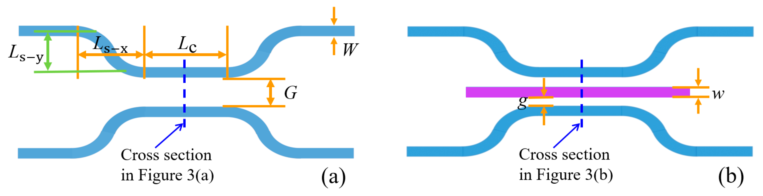
Here, the optical performance of the proposed switch is analyzed. To more accurately analyze the device performance, the three-dimensional finite-difference time-domain (3D FDTD) method is utilized for optimization, with a mesh of 0.02 µm in the
X direction, 0.05 µm in the
Y direction, and 0.01 µm in the
Z direction. Considering the calculated capacity of the computer, the waveguide roughness is set to zero. In order to achieve better performance with size reduction so as to only work under the fundamental mode, the single-mode waveguide is calculated. With an incident wavelength of 1.550 μm and waveguide height
H of 0.5 μm as an example, the effective refractive indices
neff under different waveguide widths
W are calculated as shown in
Figure 4, and the insets are the mode fields under the corresponding size.
It is found that when W < 1.4 μm, the mode supported by the waveguide is still only the fundamental mode TE0; when W ≥ 1.4 μm, the high-order mode TE1 appears. In order to reduce device size, the waveguide width W is selected to be 0.8 μm. Considering factors such as ideal coupling, simplified structure, and reduced fabrication difficulty, the size of the middle straight waveguide, 0.8 μm (w) × 0.5 μm (H), is selected.
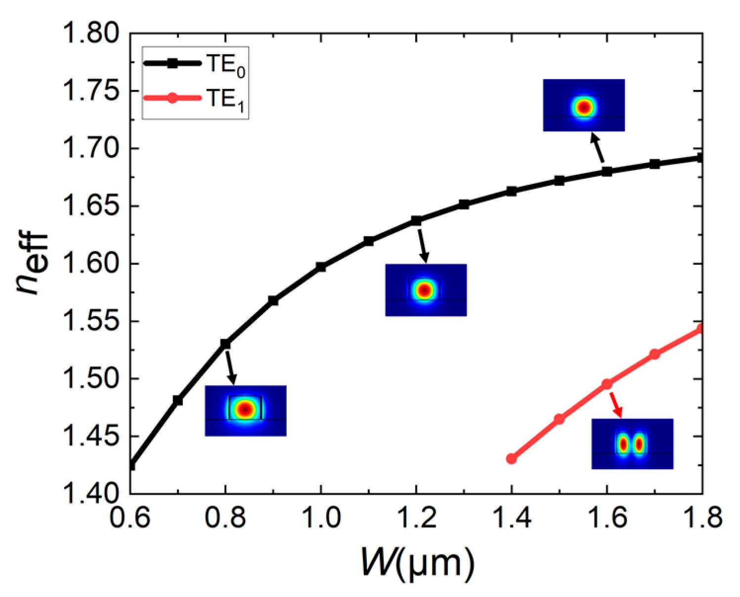
After the basic size of the waveguide is determined, in order to reduce the insertion loss of the device, the bend length of the DC curved waveguide needs to be determined. For the top view of the DC structure in
Figure 2a, it can be seen that
Ls-y and
Ls-x jointly affect the bending degree of the waveguide. In order to simplify calculation and reduce device size, when
Ls-y is selected as 2.9 μm, the relationship between transmission T of waveguide and
Ls-x is calculated, and the result is shown in
Figure 5. As shown in
Figure 5, as
Ls-x increases, the transmission of the waveguide increases. That is, as
Ls-x increases, the curvature of the waveguide becomes gentler, and the mode in the waveguide changes less. Considering the device size, when
Ls-y = 2.9 μm,
Ls-x is selected as 17 μm.
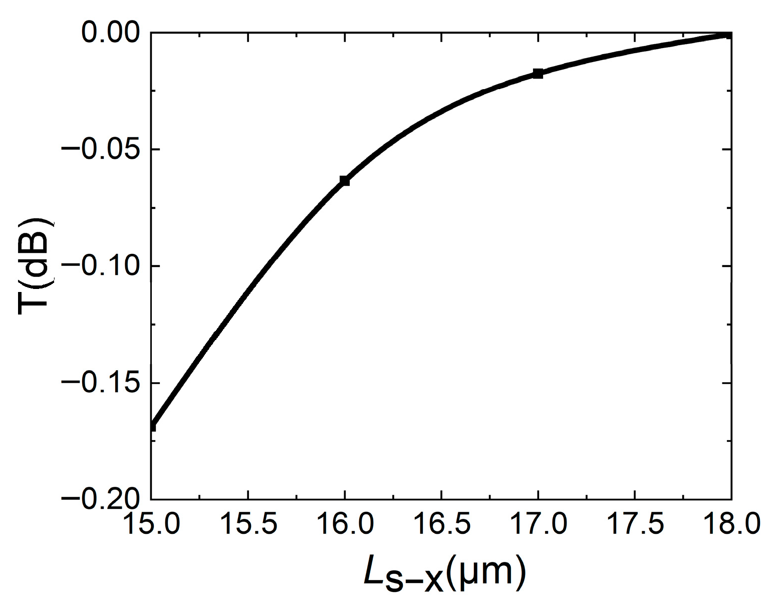
For DC structures, the key structural parameters that affect DC coupling are coupling length and coupling gap. The coupling gap should not be too small and should be selected based on the characteristic size of lithography. Otherwise, the difficulty of fabrication will increase and the fabrication parameters will not easily meet the theoretical design, thereby affecting performance. For the structural parameters in
Figure 2, since the waveguide width
W has been determined to be 0.8 μm, considering reducing the subsequent difficulty of static fabrication and device size,
g is selected as 0.25 μm, that is,
G = 2
g +
w = 1.3 μm. For a coupling gap of 1.3 μm in a DC structure, it is difficult to achieve optical coupling, so the coupling length needs to be determined under the condition that the suspended straight waveguide is pulled down. In
Figure 6, the relationship between transmissions of the bar port and cross port and the coupling length
Lc when
g = 0.25 μm is calulated. Since the straight waveguide is moved down, the larger the transmission of the cross port, the better the performance. It can be seen that the transmissions of both ports increase with increasing coupling length. This is because different coupling lengths lead to different light energies in the straight waveguide, which in turn affects the energy of two output ports.
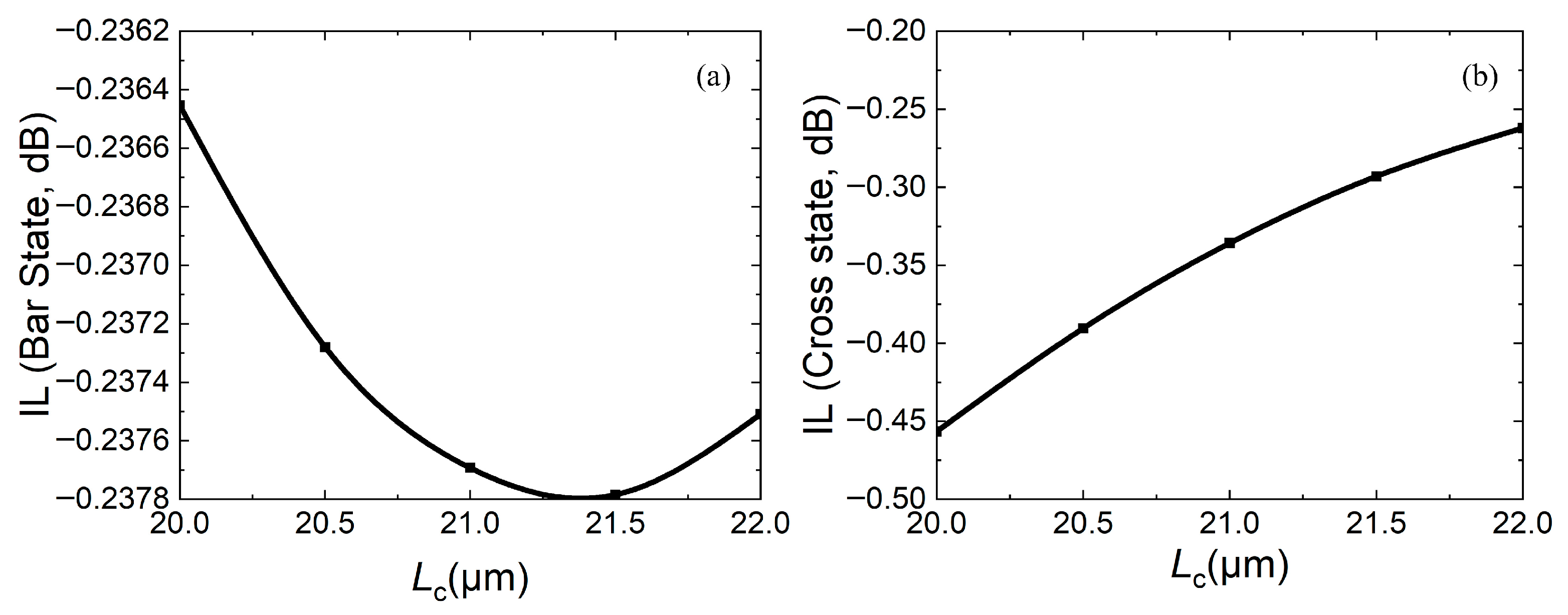
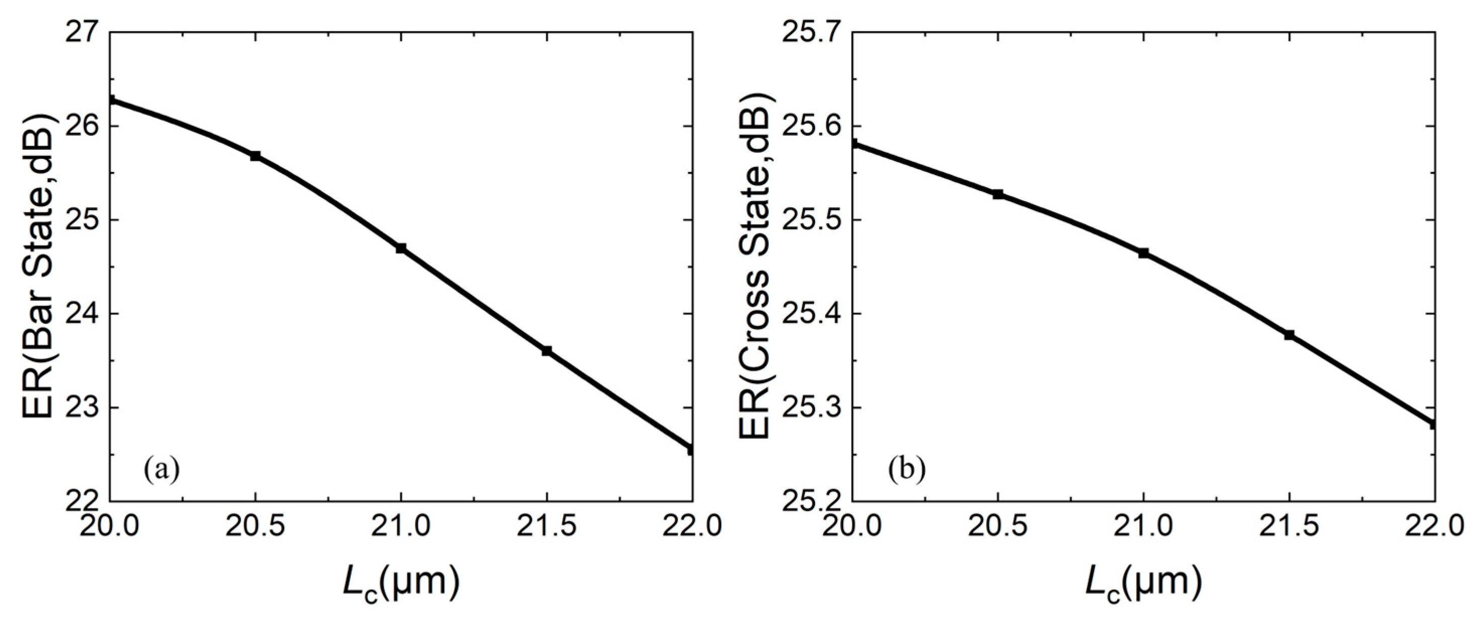
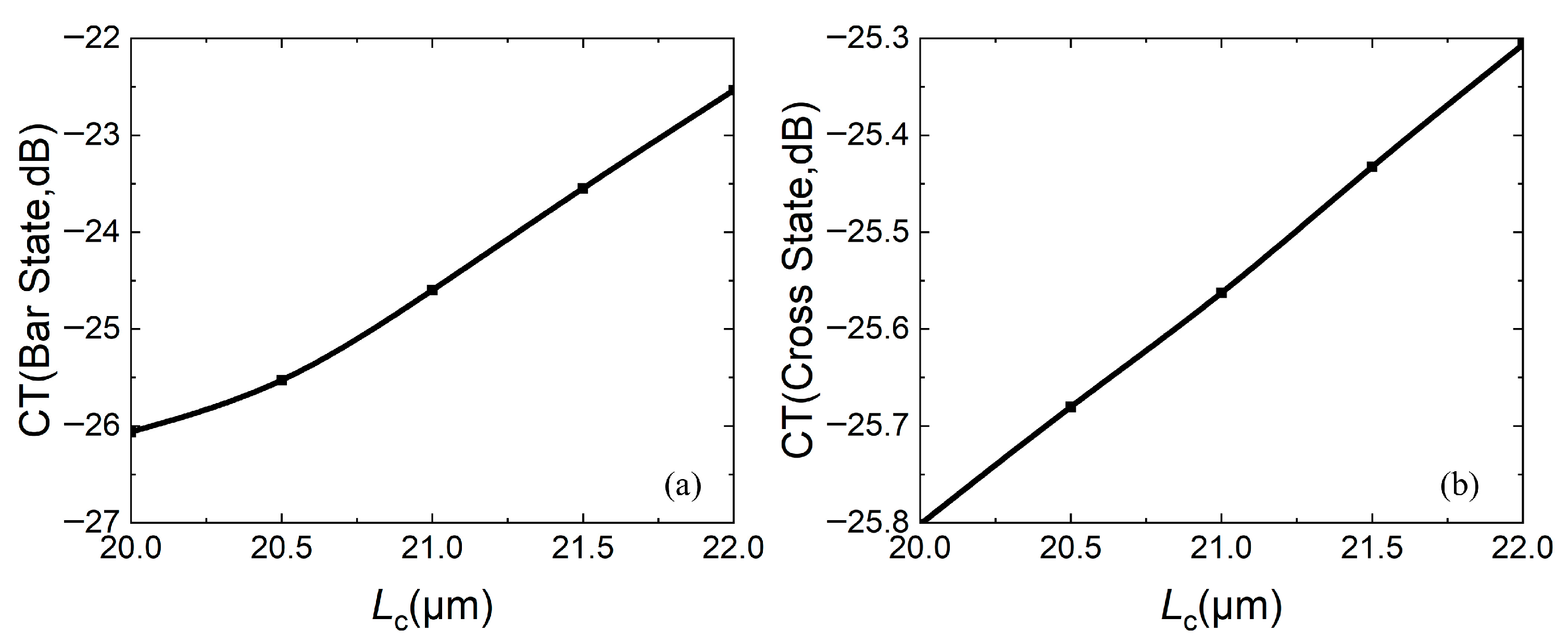
To further determine the coupling length, the relationship between the coupling length and insertion loss (IL), extinction ratio (ER), and crosstalk (CT) is calculated, as shown in
Figure 7,
Figure 8 and
Figure 9, respectively. For insertion loss, the smaller the better (expressed as an absolute value), whether the device is in the bar state or the cross state.
Figure 7a shows that as
Lc increases, insertion loss firstly increases and then decreases, while
Figure 7b shows that as
Lc increases, the insertion loss decreases. In both states, the insertion losses are less than 0.5 dB.
For the extinction ratio, the larger, the better. The larger the ER is, the better performance of the same port in switching light “on” and “off”.
Figure 8a,b both show that as
Lc increases, the ER decreases. In both states, the ERs of two ports is greater than 22 dB.
For the crosstalk, the smaller, the better. The smaller the CT is, the smaller the light energy of the port that should not exist under the same state.
Figure 9a,b both show that the CT increases with increasing
Lc. In both states, two-port CTs are less than −22 dB.
Considering comprehensively, the coupling length Lc is selected as 21 μm.
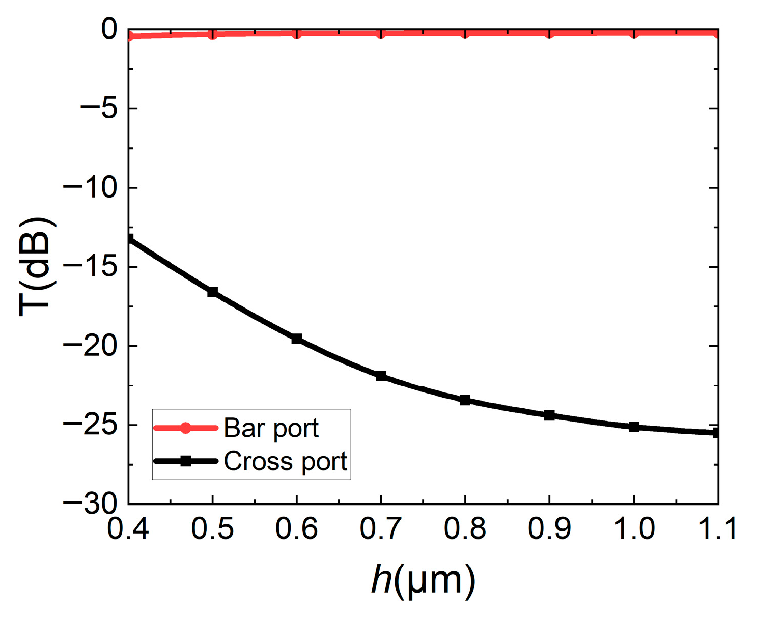
In order to further determine that the straight waveguide will not interfere with optical coupling in the bar state when it is suspended, the influence of the straight waveguide suspension height
h on the transmissions of two output ports is calculated, and the results are shown in
Figure 10. It can be seen that when the straight waveguide is suspended by 0.4 μm, the straight waveguide still has a height of 0.1 μm between the DC, causing some light to couple. As the straight waveguide suspended height gradually increases, it is difficult for optical coupling to occur between DC waveguides, the energy of the cross port gradually decreases, and the switch is in the bar state. According to the simulation results, the suspended height
h of the straight waveguide needs to be higher than 1.1 μm, at which time the suspended straight waveguide will not affect the bar state.
When the straight waveguide is pulled down, since the surface of the lower cladding layer is possibly rough, the straight waveguide may not be closely stitched to the lower cladding layer. Considering the capacity of the computer and saving calculating time, the mesh in the
Z direction is set to 0.01 μm, the analysis for the cases where stitched slot
hv measures 0.01 μm, 0.02 μm, and 0.03 μm between the straight waveguide and the lower cladding is shown in
Figure 11. It has the same trend as
Figure 10, and failure to closely stitched to the lower cladding layer will seriously affect performance. When the stitched slot is 0.01 μm, the transmissions of the cross port and bar port are 0.48 dB and 15.03 dB, respectively. Chemical mechanical polishing (CMP) needs to be used to flatten the surface of the lower cladding layer in later fabrication. At the same time, when fabricating the straight waveguide, it is also necessary to ensure that the lower surface of the waveguide is flat enough.
Based on the optimization and confirmation of the above structural parameters, the overall performance is calculated. The optical field distribution in the bar state and cross state are shown in
Figure 12a,b, respectively. The structural parameters and key performance are summarized in
Table 1. It can be seen that the optical switching function is realized by affecting DC coupling through the straight waveguide. In the bar and cross states, the insertion loss is approximately 0.24 dB and 0.33 dB, the extinction ratio is approximately 24.70 dB and 25.46 dB, and the crosstalk is approximately −24.60 dB and −25.56 dB, respectively. The device shows good optical switch performance.
By positioning the straight waveguide at up and down positions in the
Z direction, it is possible that the straight waveguide will deviate on one side of the DC waveguide in the
X direction.
Figure 13a,b analyze an optical field comparison of the straight waveguide at the down position with an upward and downward offset 0.05 μm of the DC. When the straight waveguide is offset by 0.05 μm upward, the coupling length between the DC input waveguide and the straight waveguide remains unchanged, but the coupling gap decreases, so some of the light is coupled back to the DC waveguide. At this time, the transmission of the bar port is 7.90 dB and the transmission of the cross port loss is 1.08 dB. When the straight waveguide is offset by 0.05 μm downward, similarly, the coupling gap increases, so some of the light is not coupled into the straight waveguide. At this time, the transmission of the bar port is 7.98 dB and the transmission of the cross port is 1.07 dB.
At the same time, fabrication errors are also calculated.
Figure 14,
Figure 15 and
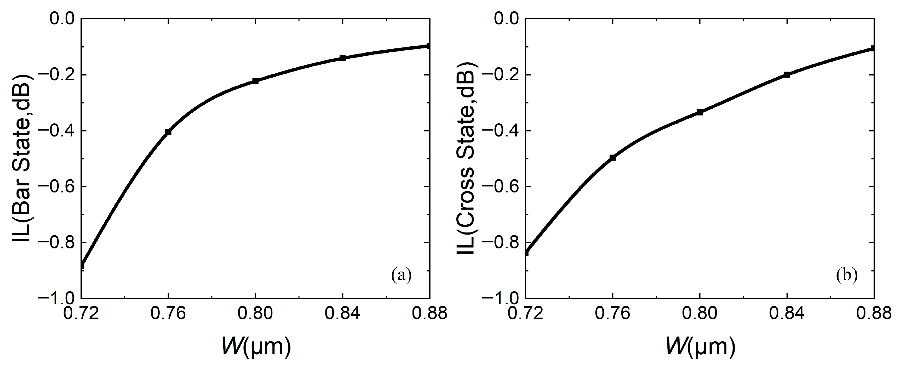
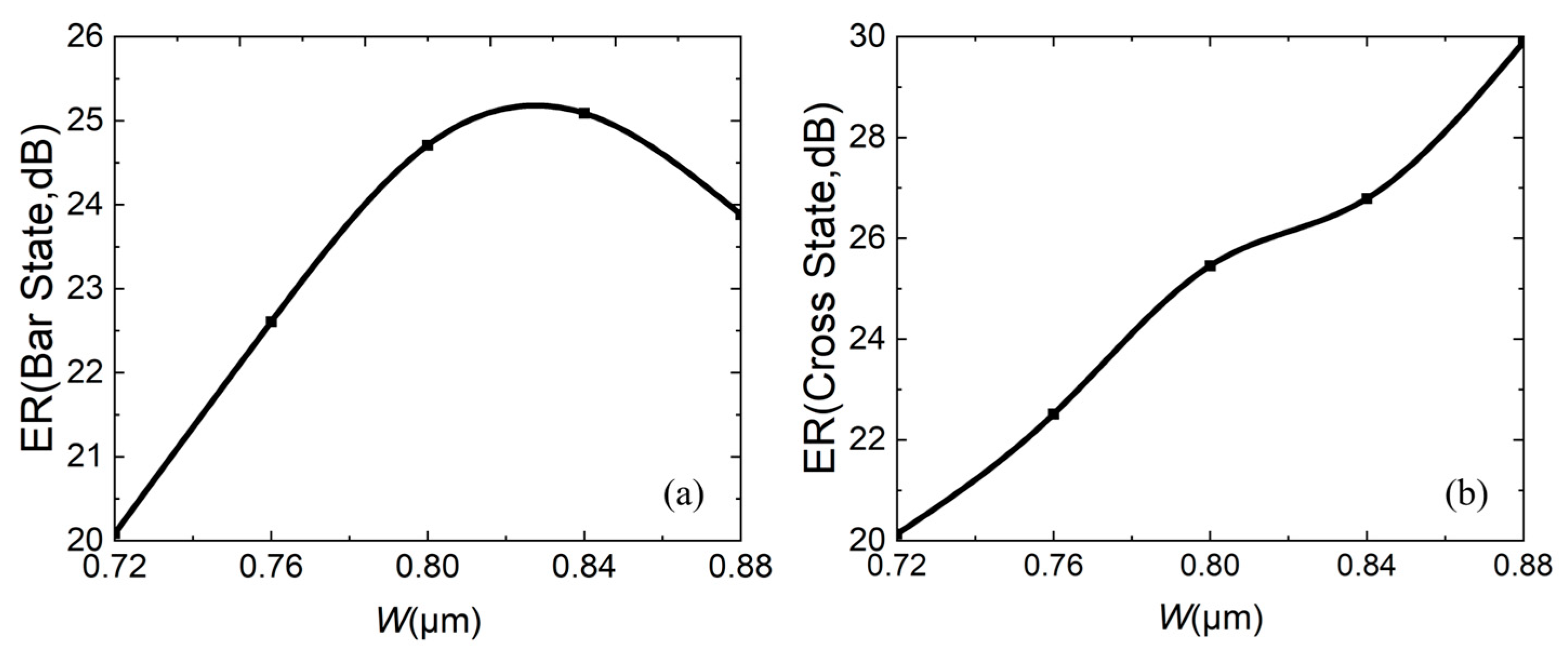
Figure 16 analyze the impact of fabrication errors at ±5% and ±10% on insertion loss, extinction ratio, and crosstalk. It should be noted that the following simulations are performed under the conditions that the waveguide width increases and the coupling gap decreases, while the waveguide width decreases and the coupling gap increases.
Figure 14a,b shows the insertion loss in the bar and cross states, respectively. It can be seen that the insertion loss decreases with increasing waveguide width, due to an increase in the mode restriction ability, and the bar state leads to reduced insertion loss. The cross state is such that the coupling efficiency between the waveguides is higher at a wider waveguide width, and there is less residual light in the straight waveguide, which leads to reduced insertion loss. If device insertion losses are less than 0.5 dB in both states, the waveguide width must be wider than 0.76 μm.
Figure 15a,b are the extinction ratios of the bar port and cross port, respectively, and
Figure 16a,b are the crosstalk of the bar port and cross port, respectively. From
Figure 15 and
Figure 16, a fabrication error of ±5% and ±10% can satisfy an extinction ratio greater than 20 dB and a crosstalk of less than −20 dB, which shows that the fabrication tolerance of the device is large. In addition, when the fabrication error is +5%, corresponding to
W = 0.84 μm and
g = 0.21 μm, it has the best comprehensive performance.
In the field of LiDAR, phase modulation can be used for horizontal scanning, and frequency (or wavelength) modulation can be used for vertical scanning. In the field of optical communications, wavelength division multiplexing (WDM) technology is often used to increase data capacity. Therefore, the optical switch needs to work with low insertion loss within a certain optical bandwidth.
Figure 17a,b calculates the insertion losses and crosstalk in the C band.
When the device is in the bar state, the straight waveguide is suspended. As the wavelength increases, the insertion loss increases, because of the material’s dispersion effect. As the wavelength increases, the device’s effective refractive index diminishes. Consequently, the waveguide’s capacity to confine light weakens, leading to heightened waveguide propagation loss. Simultaneously, the coupling length required for complete coupling shortens. Given that the actual coupling length remains fixed, a greater portion of light is coupled into the cross port, thereby resulting in increased insertion loss and crosstalk at the bar state.
When the device is in the cross state, the straight waveguide is pulled down. The same principle applies as above: the required coupling length for complete coupling is reduced, and the residual light of the straight waveguide is decreased because of shortened complete coupling and it is better coupled to the cross port. Also due to the above reason, a greater portion of light is coupled into the bar port again. Light in the cross state is coupled twice, and insertion loss and crosstalk do not change completely linearly with wavelengths, as shown in the square black dots in
Figure 17. After linear fitting, they are shown as a solid black line. As a result, the insertion loss of cross states is reduced and crosstalk enhances with increasing wavelength.
5. Feasibility and Mechanical Analysis
The operating mechanism is that the electrodes on the Si layer provide the different voltages, the electric potential difference in the two electrodes leads to electrostatic force, and the straight waveguide is pulled down. Due to the thickness of the SiO
2 layer being higher, the straight waveguide touches the SiO
2 lower cladding layer and stops. Two electrodes cannot touch. When there is no potential difference, the electrostatic force disappears. Due to the Si
3N
4 film deposited on the suspended Al top electrode to enhance the stiffness of the Al film, a suitable voltage is used without destroying the suspended electrode structure, and the electrodes can rebound to their initial position by relying on inherent stress. Stiction is less likely to occur. In addition, the suspended Si
3N
4 straight waveguide has a large aspect ratio, but there is no need to worry about deformation. Similar structures are referenced in [
31,
32].
Although the electrodes are located near the waveguides, the device is essentially unaffected by heat. This is due to the following reasons: Firstly, both Si3N4 and SiO2 are materials with low thermo-optic coefficients. Secondly, the waveguide is situated above the SiO2 lower cladding layer, and SiO2 is a material with low thermal conductivity; above the electrodes is air, whose thermal conductivity is even poorer than that of SiO2. Thirdly, there is a certain distance between the electrode and the waveguide, and the electrodes are in direct contact with the Si layer, and Si serves as an excellent heat sink. Fourthly, the switch is actuated by electrostatic attraction induced by potential difference, where the voltages of the upper and lower electrodes is different. There is no directly conducting current and no metal wires with high resistance, resulting in minimal heat generation.
For the proposed electrostatically actuated optical switch, the actuation voltage characteristics of cross and bar states are inherently distinct. Cross-state operation requires a sustained voltage to maintain the electrostatic attraction between the top and bottom electrodes, ensuring the waveguide adheres to the lower cladding. Bar state operation relies on the elastic recovery of the suspended electrode structure after the voltage is removed, requiring no additional power input. According to the structure and mechanism of the proposed switch, the stability will not be a problem and there is reliable feasibility.
The pull-in voltage
Vpi of electrostatic parallel plate actuators is described by Equation (1) [
33]. The key parameters include the stiffness
k, the overlap area
A of the parallel electrodes, and the initial gap
d0 between the electrodes.
is the permittivity of air between the electrodes. It can be seen that
Vpi is positively correlated with
k and
d0 and negatively correlated with
and
A.According to Equation (1) above, the
of air is 8.85 × 10
−12 F/m, based on the results of
Figure 10, and assuming
d0 is 1.1 μm,
A is 54 μm
2. The key factor is the
k of the suspended electrode material. In our design, the suspended top electrode material is hybrid, and the Si
3N
4 is the key element that influences the stiffness. In simplified models and calculations, only Si
3N
4 is considered. The factor
k that electrostatically actuates planar capacitive actuators with a single support structure for an edge is simplified to Equation (2):
Assume the suspending Si3N4 film has 0.1 μm thickness t, 9 μm length l, and 6 μm width w. The Young’s modulus E of Si3N4 is 290 GPa, so via Equation (2), k ≈ 0.6 N/m. Then, via Equation (1), Vpi ≈ 22.3 V.
As for one proposed structure, the resonant frequency
f can be calculated by Equation (3).
m is the mass of one side-suspended structure. It consists of two parts: one is the mass
m1 of the electrode, and the other is the mass
m2 of the straight waveguide.
m1 = (
) ×
lwt = 3.2 × 10
−14 kg, and
m2 = 6.4 × 10
−14 kg. However, the weight of the straight waveguide is borne by the two electrodes,
m =
m1 + 0.5
m2, with
f ≈ 0.5 MHz.
The resonant frequency is the natural frequency of the material and structure under specific conditions. If a device operates at this frequency, it will malfunction. Therefore, to ensure normal operation, the device’s working frequency should be less than 1/10 of the resonant frequency. Theoretically, higher resonant frequencies correspond to faster switching speeds. A rough estimate of the switching speed is the reciprocal of the resonant frequency [
34]. Based on this assessment, the switching speed may be 20 μs. Actually, switching speed is included the cross and bar times. The factors affecting the two switching times are also different. The cross time (pull-down) is mainly affected by stiffness. As for the bar time, it depends on the suspended structure’s built-in tension to snap it back to the suspended position. Damping action of air, stiffness and tension of films, and suspended height are all key factors.


