Article

The Impact of Single-Event Radiation on Latch-Up Effect in High-Temperature CMOS Devices and Its Mechanism

by
Bin Wang
,
Jianguo Cui
,
Ling Lv
* and
Longsheng Wu
State Key Laboratory of Wide Bandgap Semiconductor Technology, Faculty of Integrated Circuit, XiDian University, Xi’an 710071, China
*
Author to whom correspondence should be addressed.
Micromachines 2025, 16(7), 783; https://doi.org/10.3390/mi16070783
Submission received: 31 May 2025 / Revised: 28 June 2025 / Accepted: 29 June 2025 / Published: 30 June 2025

Abstract

This paper investigates the latch-up effect in CMOS devices based on a 28 nm CMOS process within the temperature range of 200 K to 450 K using Sentaurus Technology Computer-Aided Design (TCAD) simulation, with a particular focus on the single-event latch-up (SEL) effect in the high-temperature range of 300 K to 450 K. The physical mechanism underlying the triggering of SEL in CMOS devices at high temperatures is revealed. The results show that when the linear energy transfer (LET) value is 75 MeV cm2/mg, the CMOS devices do not exhibit SEL effects at 300 K and 350 K. However, when the temperature rises to 400 K, a significant latch-up effect occurs, which becomes more pronounced with increasing temperature. Additionally, at a supply voltage of 1.2 V and a temperature of 450 K, the LET threshold for triggering SEL in CMOS devices decreases by 91.4% compared to 75 MeV cm2/mg at 300 K, dropping to 6 MeV cm2/mg. As the temperature increases, the latch-up trigger current of the CMOS devices decreases from 1.18 × 10⁻⁴ A/μm at 300 K to 4.65 × 10⁻⁵ A/μm at 450 K, and the hold voltage decreases from 1.48 V at 300 K to 1.07 V at 450 K.

1. Introduction

In space environments such as near-Earth orbits and the lunar surface, CMOS integrated circuits are exposed to significant temperature variations. The surface facing the sun can reach temperatures above 150 °C (423 K), while the shaded side can drop to below −100 °C (173 K) [1]. However, the latch-up effect in CMOS devices is highly sensitive to temperature variations. The latch-up effect in CMOS devices at low temperatures has been extensively studied, yielding a series of meaningful results [2,3,4,5,6]. Concurrently, the single-event latch-up (SEL) effect under elevated-temperature conditions is attracting growing research interest.
In fact, as integrated circuit technology enters the deep sub-micron era, the high-temperature characteristics of MOSFET devices have changed significantly. The threshold voltage decreases, the off-state current deteriorates, the carrier mobility reduces, and the power consumption of the circuit increases, severely affecting the performance of CMOS integrated circuits and potentially causing functional failures [7]. The temperature dependence of CMOS latch-up has been widely studied. J.G. Dooley et al. investigated the temperature dependence of latch-up hold current, trigger current, and bulk resistance in CMOS devices, finding that the hold and trigger currents decrease with increasing temperature, while the CMOS bulk resistance and parasitic transistor current gain increase [8]. E. Sangiorgi et al. studied the temperature dependence of latch-up hold voltage in very large-scale integration (VLSI) CMOS technology over the range of 77 K to 400 K, observing a significant increase in CMOS parasitic bulk resistance with rising temperature, leading to an increase in hold voltage [9]. C.C. Yao et al. investigated the temperature dependence of latch-up in asymmetric lightly doped drain (LDD) CMOS, proposing that the hold current decreases with increasing temperature and the trigger voltage slightly decreases as temperature rises [10]. They also provided a relationship between the hold current, parasitic transistor current gain, and parasitic bulk resistance. Liang et al. studied the temperature characteristics of electrostatic discharge (ESD) protection devices in the high-temperature range of 300 K to 500 K, finding that the hold voltage and hold current decrease with increasing temperature, increasing the risk of latch-up in ESD protection devices at high temperatures [11]. These studies reveal that CMOS latch-up effects exhibit pronounced temperature dependence.
However, the above research exclusively addresses conventional latch-up phenomena without addressing single-particle radiation impacts. Actually, the SEL effects induced by the radiation become significantly more pronounced under elevated temperatures. A. H. Johnston et al. investigated the impact of elevated temperatures on SEL effects. The study revealed that latch-up thresholds are strongly influenced by contact geometry, with temperature dependence consistent with models based on triggering vertical parasitic transistors. At 125 °C, the linear energy transfer (LET) threshold decreased by a factor of approximately 2.5 relative to room temperature [12]. H. Iwata et al. investigated the temperature dependence of SEL phenomena in CMOS devices across the 77–450 K temperature range. The study demonstrated that CMOS immunity to SEL progressively diminishes as temperature increases from 120 K to 450 K [13]. S. Guagliardo et al. investigated the impact of temperature variations on SEL susceptibility in CMOS devices. The investigation considered three geometry and design-dependent parameters: doping profiles, anode-to-cathode (A–C) spacing, and placement of substrate/well contacts. The study revealed that temperature effects on SEL susceptibility become more pronounced in devices exhibiting lower inherent SEL sensitivity [14]. E. V. Mrozovskaya et al. experimentally investigated the relationship between SEL cross-section and LET for various CMOS circuits across different temperatures. The experimental results demonstrated that the SEL cross-section increases with elevated temperatures [15]. However, these studies have primarily focused on the impact of parameters such as CMOS device process manufacturing, doping profiles, and anode-to-cathode spacing on SEL effects, while the physical mechanisms triggering SEL in CMOS devices at elevated temperatures have not been sufficiently explored. Furthermore, with the continued scaling of CMOS device feature sizes, the characteristics of 28 nm process CMOS devices under single-particle irradiation differ significantly from those with larger feature sizes [16].
Therefore, this paper investigates the high-temperature characteristics of single-event latch-up in CMOS devices based on the 28 nm process over the temperature range of 300 K to 450 K, using Sentaurus TCAD simulation to reveal the physical mechanism underlying the triggering of SEL in CMOS devices at high temperatures based on the generation and recovery processes of excess carriers. The study also explores the sensitivity factors of SEL effects.

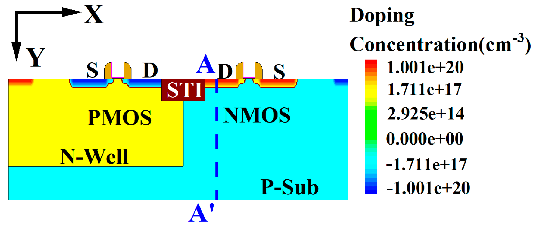
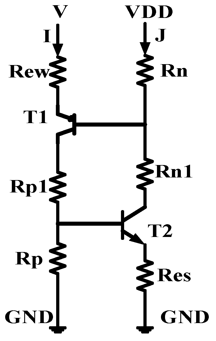
2. Device Parameters and Model Establishment

Figure 1 shows the structure of the CMOS device, with parameters designed based on 28 nm CMOS technology. The P-type substrate doping concentration is 1 × 1016 cm−3, the N-Well doping concentration is 1 × 1018 cm−3, and the source and drain doping concentrations of both NMOS and PMOS are 1 × 1020 cm−3. Detailed parameters are listed in Table 1.
Figure 2 illustrates the equivalent circuit diagram of the CMOS single-event latch-up effect [17,18]. Rn and Rp represent the parasitic bulk resistances of the N-Well and P-substrate, respectively, while Rn1 and Rp1 are the internal extended resistances of the N-Well and P-substrate, which act as shunts for the emitter junctions. T1 and T2 are the parasitic transistors within the well and substrate. To study the SEL effect in high-temperature environments, a heavy ion model was added to the Sentaurus TCAD software. A single heavy ion is incident on the sensitive region of the NMOS drain when the CMOS device input is at low voltage [19]. The ion incidence direction is along the positive Y-axis, with a radiation time of 1 × 10⁻¹¹ s. The A-A’ cutline indicates the direction along the heavy ion incidence. Additionally, the following models were included: Fermi model, bandgap narrowing model, SRH (Shockley–Read–Hall recombination) and Auger recombination models, high-field saturation effect model, doping-dependent scattering, interface scattering, and carrier–carrier scattering [13,14].

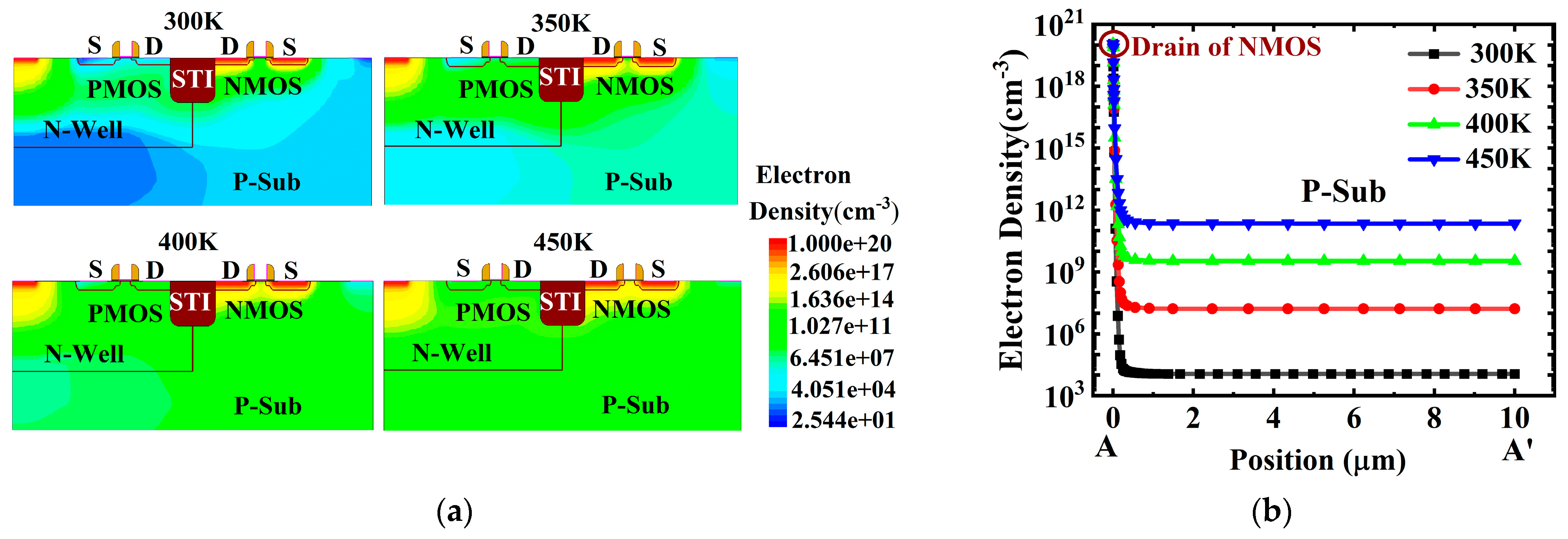
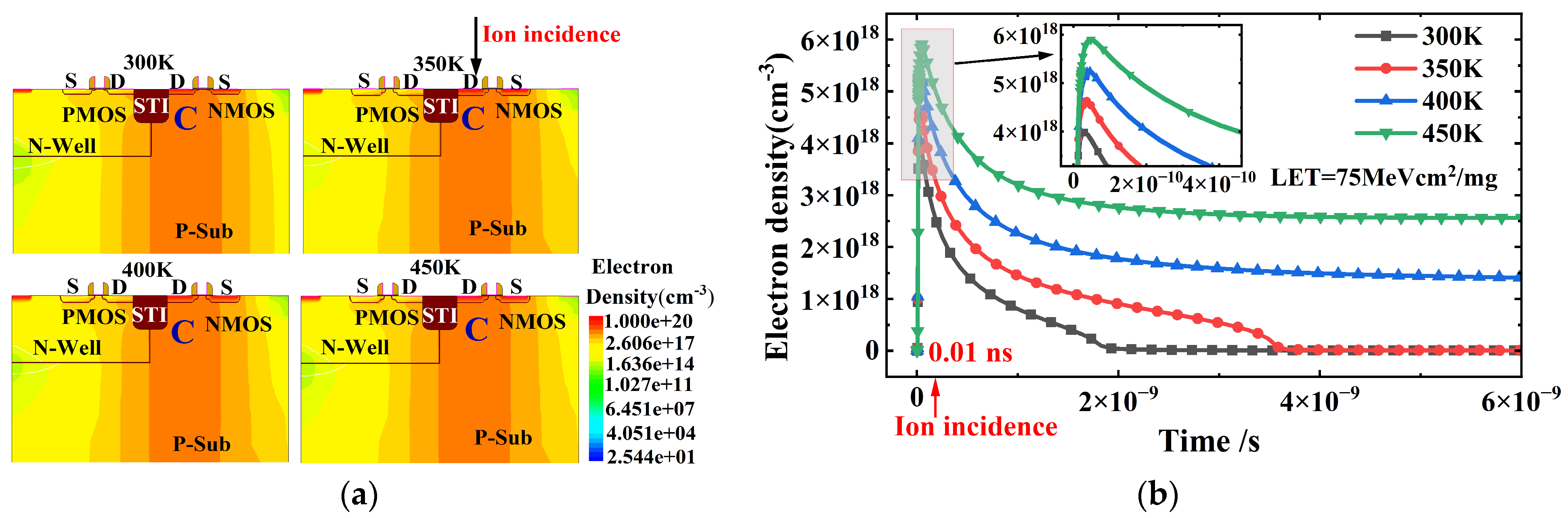
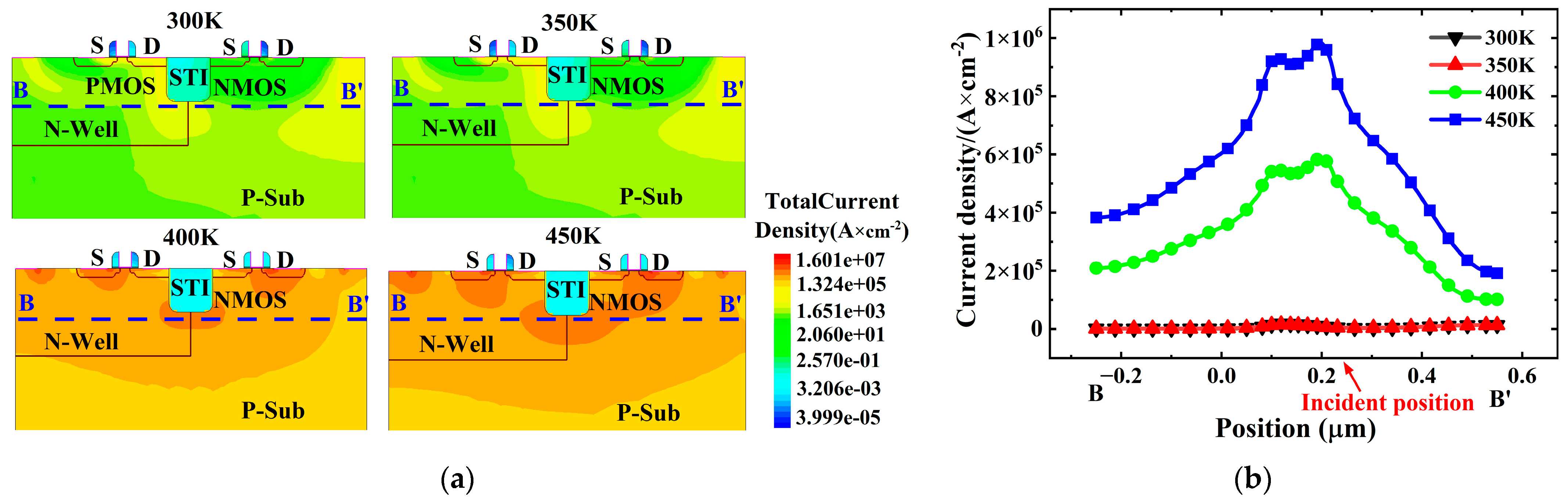
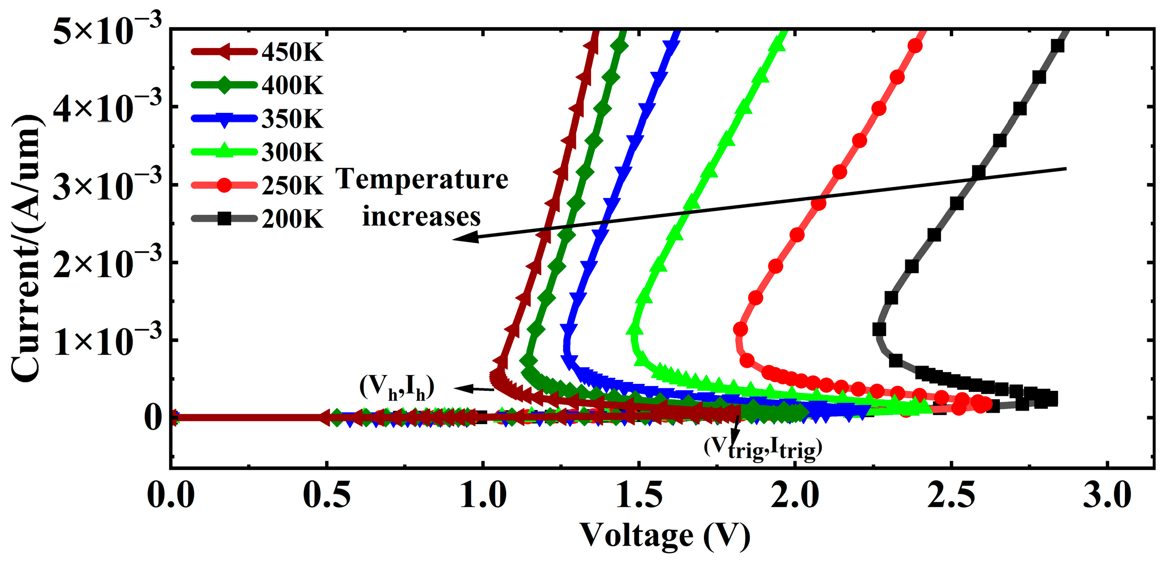
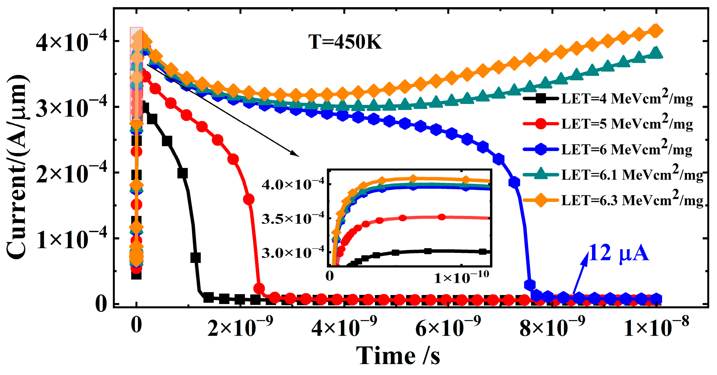
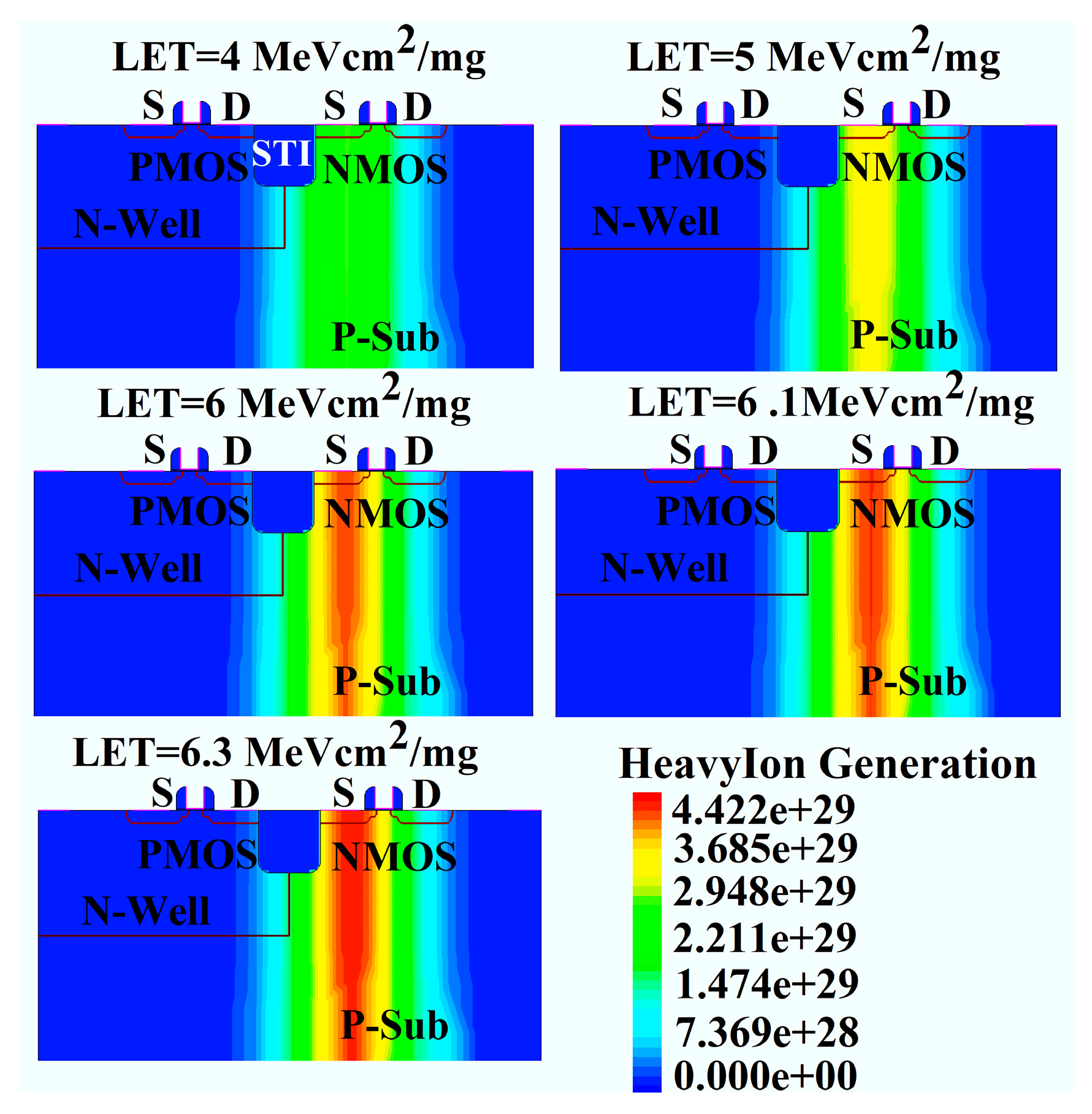
3. Simulation Results and Analysis

Figure 3 describes the impact of single-event radiation on the latch-up effect in CMOS devices at different temperatures ranging from 300 K to 450 K. The LET value of the heavy ion is 75 MeV cm2/mg, and the supply voltage is 1.2 V. At 0.01 ns, a heavy ion strikes the drain side of the NMOS, and the internal current of the CMOS device is monitored after the ion strike. The transient scan duration is 6 ns. Before the heavy ion incidence (t < 0.01 ns), the internal current of the CMOS device remains at the μA level. After the ion incidence (t = 0.01 ns), a transient current pulse appears due to the generation of a large number of non-equilibrium carriers, as shown in Figure 3. At 300 K, the peak pulse current is 2.0 mA, and it increases to 2.1 mA at 350 K, 2.2 mA at 400 K, and 2.4 mA at 450 K with rising temperature. Additionally, the pulse current at 300 K and 350 K returns to the μA level before ion incidence (t < 0.01 ns) after 2 ns and 3.5 ns, respectively, indicating that the latch-up effect does not occur. However, when the temperature rises to 400 K and 450 K, the pulse current remains at the 10−4 level after 6 ns, significantly higher than the current before ion incidence, resulting in a tail current (latch-up current), indicating that the latch-up effect is triggered. Moreover, the latch-up current at 450 K is 9.5 × 10⁻⁴ A/μm, higher than the latch-up current at 400 K (5.6 × 10⁻⁴ A/μm), demonstrating that the SEL effect becomes more pronounced with increasing temperature. The reasons why the SEL effect is more severe at high temperatures are mainly twofold. First, the concentration of non-equilibrium carriers generated by single-particle irradiation increases significantly at high temperatures. Second, the latch-up threshold of CMOS devices decreases with the rise in temperature. The following analysis will focus on these two aspects.
Figure 4 depicts the electron distribution within the device at different temperatures ranging from 300 K to 450 K before ion incidence (t = 0.005 ns). At t = 0.005 ns, carriers drift under the influence of the supply voltage. Due to the decrease in ionization energy with increasing temperature, the electron density in the P-Sub region increases from 104 cm−3 at 300 K to 1011 cm−3 at 450 K, as illustrated in Figure 4, increasing the current before ion incidence (t = 0.005 ns). Figure 5 shows the electron distribution within the device at different temperatures ranging from 300 K to 450 K after ion incidence (t = 0.01 ns). At t = 0.01 ns, a large number of excess carriers are generated within the ion incidence track, and the concentration of excess carriers increases significantly with rising temperature, from 4.0 × 1018 cm−3 at 300 K to 6 × 1018 cm−3 at 450 K, as shown in Figure 5. The large number of excess carriers generated by irradiation creates a transient current pulse, as shown in Figure 3. Since the pulse current is positively correlated with the concentration of excess carriers, the peak pulse current increases significantly from 2.1 mA to 2.4 mA with rising temperature, as shown in Figure 3.
Figure 5b describes the variation in excess carrier concentration at point C concerning time. The variation in current within the device, as shown in Figure 3, is consistent with the variation in excess carriers generated by irradiation. At 300 K, the excess carriers return to equilibrium after 2 ns. Therefore, the pulse current at 300 K decreases from a peak of 2.1 mA to the μA level before irradiation after 2 ns. As the recovery time of excess carriers increases with their concentration, the recovery time at 350 K increases to 3.5 ns. When the temperature rises to 400 K and 450 K, the carrier concentration remains at the 1018 level after irradiation, significantly higher than the carrier concentration before irradiation. The high concentration of excess carriers triggers the parasitic thyristor in the CMOS structure, causing the latch-up effect and forming a latch-up current. Moreover, the latch-up current at 450 K is higher than that at 400 K due to the higher carrier concentration after irradiation, as shown in Figure 3.
Figure 6 shows the current density distribution within the CMOS device at different temperatures ranging from 300 K to 450 K after ion incidence (t = 6 ns). At 300 K and 350 K, the device returns to equilibrium, and the current density after irradiation is 101 A × cm−2, indicating that the latch-up effect does not occur. However, when the temperature rises to 400 K, the current density along the B-B′ cutline increases significantly, with the highest current density near the ion incidence point, forming a latch-up current. Moreover, the current density at 450 K increases significantly with rising temperature, leading to a more severe latch-up effect, as shown in Figure 6. This proves that the SEL effect in CMOS devices is positively correlated with temperature.
Figure 7 shows the equivalent circuit diagram of the lumped element model for CMOS latch-up [20]. The trigger voltage, trigger current, hold voltage, and hold current can be calculated from the equivalent circuit as follows:
V t r i g = V D D + V b i 1 + V b i 2 × R e w R p × P N P
I t r i g = V b i 2 R p × P N P    
I h = R e s × V D D + R e s × V b i 1 + R n × V b i 2 R e s × P N P R p + R p 1 + P N P R p + R n  
V h = I h × R e w + R p × P N P + R p 1 × P N P + V C E 1 V b i 2 × 1 + R P 1 R p + V C E 1
where β is the common-base current gain of the PNP transistor; RP, Rn, Res, and Rew are the parasitic bulk resistances of the CMOS device; VCE1 is the saturation voltage of the PNP transistor; and Vbi1 and Vbi2 are the built-in potentials of the emitter junctions of the parasitic transistors T1 and T2. Since the parasitic bulk resistance and transistor current gain have positive temperature coefficients, while the built-in potential has a negative temperature coefficient, the latch-up trigger voltage (Vtrig), trigger current (Itrig), hold current (Ih), and hold voltage (Vh) all decrease with increasing temperature.
Figure 8 illustrates the I-V characteristic curve of the CMOS latch-up effect over the temperature range of 200 K to 450 K. The point where the device transitions from the high-resistance off-state to the negative resistance region is the trigger point, corresponding to the trigger current (Itrig) and trigger voltage (Vtrig). The point where the device transitions from the negative resistance region to the latch-up region is the hold point, corresponding to the hold voltage (Vh) and hold current (Ih). The trigger current and hold voltage determine whether the latch-up effect occurs. As the temperature increases from 200 K to 450 K, the latch-up trigger current, trigger voltage, hold voltage, and hold current all decrease, as shown in Figure 8.
Table 2 presents the simulation results of Itrig, Vtrig, Vh, and Ih over the temperature range of 200 K to 450 K. As the temperature increases, Itrig decreases from 1.18 × 10⁻⁴ A at 300 K to 4.65 × 10⁻⁵ A at 450 K, while Vh decreases from 1.48 V at 300 K to 1.07 V at 450 K. The reduction in latch-up threshold increases the risk of latch-up occurrence in CMOS devices at high temperatures. The supply voltage of 1.2 V is lower than the hold voltage (Vh) at 300 K and 350 K, failing to reach the latch-up threshold at these temperatures. Consequently, the pulse current induced by irradiation decays to the μA level after 2 ns and 3.5 ns, respectively, without triggering latch-up. However, as the temperature rises to 400 K and 450 K, the hold voltage (Vh) drops to 1.18 V and 1.07 V, respectively. The supply voltage of 1.2 V then reaches the latch-up threshold, thereby triggering the latch-up effect, which becomes more pronounced with increasing temperature, as shown in Figure 3.
Following the heavy ion strike, the carrier generation function of the device follows the Gaussian distribution with a 10 nm radius and characteristic time of (TC = 10 ps) [21]. LET represents the charge deposition per unit length along the radiation track, with units of MeV·cm2/mg. The impact of heavy ions is carried out through another parameter known as ion generation rate (Grion). It is calculated by mathematical expressions.
G r i o n = G r L E T × R i O N × T i O N  
Here, GrLET is the LET density, and RiON and TiON are functions for spatial and temporal distribution of the generation rate, respectively:
G r L E T = 1 π r 0 2 L E T _ f ( l )
R i O N r , l = e x p r r 0 2
T i O N t = 2 exp t t 0 2 W 0 2 2 W 0 π 1 + erf t 0 2 W 0
LET_f is defined as the heavy ion model in picoCoulombs, r is the perpendicular radial distance from the ion track, t is time, and r0 and W0 are characteristic parameters of the Gaussian function [22,23,24].
Figure 9 describes the SEL effect in CMOS devices at 450 K for different LET values, namely 4 MeV cm2/mg, 5 MeV cm2/mg, 6 MeV cm2/mg, 6.1 MeV cm2/mg, and 6.3 MeV cm2/mg. When the LET is 4 MeV cm2/mg and 5 MeV cm2/mg, the pulse current returns to the μA level before ion incidence (t < 0.01 ns) after 1.6 ns and 2.1 ns, respectively, without triggering the latch-up effect. According to Equation (6), the concentration of excess carriers generated by heavy ions in silicon increases with the increasing LET value, as shown in Figure 10. Therefore, the transient current at 6 MeV cm2/mg is significantly higher than that at 4 MeV cm2/mg and 5 MeV cm2/mg, and the pulse current duration increases to 8 ns. However, the stable current value at 6 MeV cm2/mg is 12 μA/μm, higher than that at 4 MeV cm2/mg and 5 MeV cm2/mg. When the LET value further increases to 6.1 MeV cm2/mg and 6.3 MeV cm2/mg, the high concentration of excess carriers triggers the parasitic positive feedback loop in the CMOS structure, causing a sharp increase in current and triggering the latch-up effect, with the latch-up current increasing with the increasing LET value. Therefore, once the LET value of the incident heavy ion exceeds 6 MeV cm2/mg, the CMOS device will experience latch-up. Compared to the 75 MeV cm2/mg LET value at 300 K, which did not trigger latch-up, the latch-up LET threshold decreases by 91.4%.

4. Conclusions

This paper reveals the physical mechanism of the temperature dependence of latch-up effects in CMOS devices by deriving expressions for the latch-up trigger voltage, trigger current, hold voltage, and hold current. It also investigates the SEL effect in CMOS devices at high temperatures. The results show that LET value, supply voltage, and temperature are key factors in inducing the SEL phenomenon. With the continuous evolution of semiconductor technology and integrated circuit design, supply voltages are trending downward. For example, at the 28 nm process node, the supply voltage can be reduced to 1.2 V. Although low supply voltage helps protect against latch-up effects, rising temperatures, such as when a spacecraft moves from the shaded side to the sunlit side or when automotive-grade chips experience temperature increases during vehicle operation, can decrease the trigger current and hold voltage, thereby increasing latch-up sensitivity and severely affecting chip reliability. These in-depth analyses and discussions are of great significance for understanding and preventing SEL effects in CMOS devices at high temperatures.

Author Contributions

Conceptualization, B.W. and L.L. Investigation and writing—original draft preparation, B.W. and J.C. Supervision, L.W. All authors have read and agreed to the published version of the manuscript.

Funding

This research received no external funding.

Data Availability Statement

The original contributions presented in this study are included in the article. Further inquiries can be directed to the corresponding author(s).

Conflicts of Interest

The authors declare no conflict of interest.

References

  1. Ning, X.W.; Li, J.D.; Wang, Y.Y.; Jiang, F. Review on construction of new spacecraft thermal control system in China. Acta Aeronaut. Tronautica Sin. 2019, 40, 022874. [Google Scholar] [CrossRef]
  2. Marshall, C.J.; Marshall, P.W.; Ladbury, R.L.; Waczynski, A.; Arora, R.; Foltz, R.D.; Cressler, J.D.; Kahle, D.M.; Chen, D.; Delo, G.S.; et al. Mechanisms and Temperature Dependence of Single Event Latchup Observed in a CMOS Readout Integrated Circuit from 16–300 K. IEEE Trans. Nucl. Sci. 2010, 57, 3078–3086. [Google Scholar] [CrossRef]
  3. Al Youssef, A.; Artola, L.; Ducret, S.; Hubert, G.; Perrier, F. Investigation of Electrical Latchup and SEL Mechanisms at Low Temperature for Applications Down to 50 K. IEEE Trans. Nucl. Sci. 2017, 64, 2089–2097. [Google Scholar] [CrossRef]
  4. Youssef, A.A.; Artola, L.; Ducret, S.; Hubert, G.; Perrier, F. Analysis of low temperature on single event Latchup mechanisms by TCAD simulations for applications down to 50K. In Proceedings of the 2016 16th European Conference on Radiation and Its Effects on Components and Systems (RADECS), Bremen, Germany, 19–23 September 2016; pp. 1–5. [Google Scholar] [CrossRef]
  5. Deferm, L.; Simoen, E.; Dierickx, B.; Claeys, C. Anomalous latch-up behavior of CMOS at liquid helium temperatures. Cryogenics 1990, 30, 1051–1055. [Google Scholar] [CrossRef]
  6. Serbulova, K.; Qiu, S.Z.-N.; Chen, A.; Grill, K.; Kao, K.-H.; Boeck, J.D.; Groeseneken, G. Insight into Latchup Risk in 28nm Planar Bulk Technology for Quantum Computing Applications. In Proceedings of the 2024 IEEE International Reliability Physics Symposium (IRPS), Grapevine, TX, USA, 14–18 April 2024; pp. 1–7. [Google Scholar] [CrossRef]
  7. Yao, C.; Thou, J.; Cheung, R.; Chan, H. Temperature Dependence of CMOS Device Reliability. In Proceedings of the 24th International Reliability Physics Symposium, Anaheim, CA, USA, 1–3 April 1986; pp. 175–182. [Google Scholar] [CrossRef]
  8. Dooley, J.G.; Jaeger, R.C. Temperature dependence of latchup in CMOS circuits. IEEE Electron Device Lett. 1984, 5, 41–43. [Google Scholar] [CrossRef]
  9. Sangiorgi, E.; Johnston, R.L.; Pinto, M.R.; Bechtold, P.F.; Fichtner, W. Temperature dependence of latch-up phenomena in scaled CMOS structures. IEEE Electron Device Lett. 1986, 7, 28–31. [Google Scholar] [CrossRef]
  10. Yao, C.C.; Tzou, J.J.; Cheung, R.; Chan, H. Temperature dependence of latch-up characteristics in LDD CMOS devices. IEEE Electron Device Lett. 1986, 7, 92–94. [Google Scholar] [CrossRef]
  11. Liang, W.; Dong, A.; Li, H.; Miao, M.; Liou, J.J.; Kuo, C.-C.; Klebanov, M. Characteristics of ESD protection devices operated under elevated temperatures. In Proceedings of the 2016 IEEE International Nanoelectronics Conference (INEC), Chengdu, China, 9–11 May 2016; pp. 1–2. [Google Scholar] [CrossRef]
  12. Johnston, A.H.; Hughlock, B.W.; Baze, M.P.; Plaag, R.E. The effect of temperature on single-particle latchup. IEEE Trans. Nucl. Sci. 1991, 38, 1435–1441. [Google Scholar] [CrossRef]
  13. Iwata, H.; Ohzone, T. Numerical simulation of single event latchup in the temperature range of 77–450 K. IEEE Trans. Nucl. Sci. 1995, 42, 148–154. [Google Scholar] [CrossRef]
  14. Guagliardo, S.; Wrobel, F.; Aguiar, Y.Q.; Autran, J.L.; Leroux, P.; Saigné, F.; Pouget, V.; Touboul, A.D. Effect of Temperature on Single Event Latchup Sensitivity. In Proceedings of the 2020 15th Design & Technology of Integrated Systems in Nanoscale Era (DTIS), Marrakech, Morocco, 1–3 April 2020; pp. 1–5. [Google Scholar] [CrossRef]
  15. Mrozovskaya, E.V.; Chubunov, P.A.; Iakovlev, S.; Zebrev, G.I. Investigation and Simulation of SEL Cross Sections at Different Temperatures. IEEE Trans. Nucl. Sci. 2022, 69, 1587–1592. [Google Scholar] [CrossRef]
  16. Chiang, T.-H.; Huang, C.-Y.; Lin, W.-J.; Lee, J.-W.; Chen, K.-J.; Song, M.-H. Single Event Latch-up (SEL) Rate Prediction Methodology in Bulk FinFET Technology. In Proceedings of the 2024 46th Annual EOS/ESD Symposium (EOS/ESD), Reno, NV, USA, 1–3 April 2024; pp. 1–6. [Google Scholar] [CrossRef]
  17. Fang, R.C.-Y.; Moll, J.L. Latchup model for the parasiticp-n-p-n path in bulk CMOS. IEEE Trans. Electr. Dev. 1984, 31, 113–120. [Google Scholar] [CrossRef]
  18. Bruguier, G.; Palau, J.-M. Single particle-induced latchup. IEEE Trans. Nucl. Sci. 1996, 43, 522–532. [Google Scholar] [CrossRef]
  19. Jiang, M.; Fu, G.; Wan, B.; Jia, M.; Qiu, Y. Research on single event latch-up effect of CMOS based on TCAD. In Proceedings of the 2017 Second International Conference on Reliability Systems Engineering (ICRSE), Beijing, China, 10–12 July 2017; pp. 1–5. [Google Scholar] [CrossRef]
  20. Sangiorgi, E.C.; Pinto, M.R. Two-Dimensional Numerical Analysis of Latchup in a VLSI CMOS Technology. IEEE Trans Comput.-Aided Des. 1985, 4, 561–574. [Google Scholar] [CrossRef]
  21. TCAD Sentaurus User Guide; Synop. Inc.: Mountain View, CA, USA, 2022.
  22. Tiwari, S.; Saha, R.; Gopal, G.; Varma, T. Sensitivity Analysis of Ge Source Double Gate TFET Under Heavy Ion Irradiation. IEEE Sens. J. 2024, 24, 36730–36736. [Google Scholar] [CrossRef]
  23. Maurya, A.; Koley, K.; Kumar, J.; Kumar, P. Investigation of single-event-transient effects induced by heavy-ion in all-silicon DG-TFET. IEEE Access 2022, 10, 109357–109365. [Google Scholar] [CrossRef]
  24. Wang, Y.; He, X.-W.; Shan, C. A simulation study of SOI like bulk silicon MOSFET with improved performance. IEEE Trans. Electron Dev. 2014, 61, 3339–3344. [Google Scholar] [CrossRef]
Figure 1. Structure of the CMOS device.
Micromachines 16 00783 g001
Figure 2. Equivalent circuit diagram of the CMOS single-event latch-up effect.
Micromachines 16 00783 g002
Figure 3. Current–time characteristic curves of single-event latch-up at 300–450 K.
Micromachines 16 00783 g003
Figure 4. The electron distribution within the device at different temperatures ranging from 300 K to 450 K before ion incidence (t = 0.005 ns): (a) the electron density of the CMOS device; (b) the electron density of the CMOS device along the cutline A-A′.
Micromachines 16 00783 g004
Figure 5. The electron distribution within the device at different temperatures ranging from 300 K to 450 K after ion incidence (t = 0.01 ns): (a) the electron density of the CMOS device; (b) the variation curves of electron density at point C for time.
Micromachines 16 00783 g005
Figure 6. The total current density of CMOS device at different temperatures ranging from 300 K to 450 K after ion incidence (t = 6 ns): (a) the total current density of CMOS device; (b) the total current density of CMOS device along the cutline B-B′.
Micromachines 16 00783 g006
Figure 7. The equivalent circuit diagram of the lumped element model for CMOS latch-up.
Micromachines 16 00783 g007
Figure 8. I–V characteristic curves of CMOS latch-up at different temperatures ranging from 200 K to 450 K.
Micromachines 16 00783 g008
Figure 9. Current–time characteristic curves applying different LET values at 450 K.
Micromachines 16 00783 g009
Figure 10. The distribution of the heavy ion generation applying different LET values at 450 K.
Micromachines 16 00783 g010
Table 1. Parameters of the CMOS device.
ParametersValues
Length of gate28 nm
Source doping concentration 1 × 1020 cm−3
Drain doping concentration 1 × 1020 cm−3
LDD concentration 1 × 1019 cm−3
N-Well concentration 1 × 1018 cm−3
P-Sub concentration 1 × 1016 cm−3
Thickness of gate SiO21 nm
Thickness of gate HfO23 nm
Junction depth20 nm
Thickness of silicon10 um
Thickness of N-Well200 nm
Table 2. Parameters of characteristic curves at different temperatures.
Temperature (K)Itrig (A/μm)Vtrig (V)Vh (V)Ih (A/μm)
4504.65 × 10−51.81data4.02 × 10−4
4006.85 × 10−52.021.185.75 × 10−4
3509.14 × 10−52.211.277.28 × 10−4
3001.18 × 10−42.411.489.15 × 10−4
2501.72 × 10−42.601.821.03 × 10−3
2002.47 × 10−42.822.261.21 × 10−3
Disclaimer/Publisher’s Note: The statements, opinions and data contained in all publications are solely those of the individual author(s) and contributor(s) and not of MDPI and/or the editor(s). MDPI and/or the editor(s) disclaim responsibility for any injury to people or property resulting from any ideas, methods, instructions or products referred to in the content.

