3.1. Fundamental Principle of Self-Masking Micro-Fabrication Strategy
The core principle of the QMEMS adaptive 3D mask sidewall electrode fabrication strategy is to use the beam structure formed by quartz etching as the mask layer of the discrete sidewall electrodes, enabling their fabrication through secondary coating, photolithographic patterning, and the wet etching process.
Figure 5 illustrates a schematic diagram of the adaptive 3D mask sidewall electrode fabrication strategy.
For clarity in characterizing the etching topography, the length definitions are induced: the length of the bottom of the etching groove (i.e., the 3D self-masking beam) is denoted by ; and represent the thickness and length of the junction between the 3D mask beam and the vibration beams, respectively; corresponds to the wafer thickness; and indicates the etching depth. In practical application, an appropriate initial hard mask width is selected based on the wafer thickness and the etching evolution results. After the etching grooves are patterned, a double-sided etching process is performed to form an H-type beam with a controlled thickness. At this stage, both ends of the mask beam remain connected to the vibration beams. Due to the presence of the junction thickness , the mask beam can serve as a 3D sidewall electrode mask. Subsequently, a metal film is deposited again onto the substrate via deposition for sputtering to form a secondary hard mask layer. After patterning, the metal layer on the self-masking beam is selectively removed, and both the vibration beams and mutually discrete 3D sidewall electrodes are simultaneously obtained.
It is evident that this eliminates shadow mask and mechanical alignment structures. Alignment relies solely on the mark point patterned onto the wafer, meaning the lithography accuracy directly determines the alignment accuracy of the sidewall electrodes. As a result, the achievable alignment precision is significantly higher than that of the shadow mask method. Typically, lithography offers at least one order of magnitude greater alignment accuracy compared to shadow mask techniques, while also providing superior theoretical resolution limits, thereby greatly enhancing fabrication precision. Furthermore, this strategy removes the need for complicated manual alignment and the fixture assembly process, thereby improving production efficiency and yield. In addition, by eliminating the limitations imposed by the stainless-steel shadow mask’s processing tolerances, this method enables the fabrication of 3D sidewall electrodes within the ultra-high-aspect-ratio etching grooves. By employing a finely controlled hard mask width with innovative undercut processes, the obstacles to miniaturizing the out-of-plane vibration unit are effectively overcome. Finally, the size of the resulting sidewall electrodes can be adaptively controlled by adjusting the etching depth of the self-masking beam.
Figure 6 shows the entire process flow of the QMEMS adaptive 3D mask sidewall electrode fabrication strategy. Initially, the wafer surface is cleaned with strong acids and organic solvents. After surface treatment, an Au/Cr mask layer is deposited on both sides of the wafers using vapor deposition or magnetron sputtering (
Figure 6a). Next, a photoresist layer is spin-coated onto the wafer (
Figure 6b), followed by the first round of double-sided photolithography and development (
Figure 6c). The metal hard mask layer is patterned (
Figure 6d), and the photoresist is removed (
Figure 6e). The wafer is immerged in an etching solution to make the self-masking beam. The corresponding etching depth is selected based on the design of the sidewall electrodes (
Figure 6f). Subsequently, the metal mask layer is removed (
Figure 6g). After washing, the metal mask layer is re-deposited for the secondary etching process (
Figure 6h). A new photoresist is sprayed onto the wafer (
Figure 6i), followed by secondary photolithography and development (
Figure 6j). The secondary metal layer is etched to pattern the metal mask (
Figure 6k), and the photoresist is stripped (
Figure 6l). The wafer is then placed in the etching solution once more to remove the self-masking beam through secondary etching. In this process, the Au/Cr film acts as the hard mask on the quartz substrate (
Figure 6m). The wafer is coated with photoresist again (
Figure 6m) and the surface electrodes are patterned (
Figure 6n). Finally, the photoresist is stripped and the wafer cleaned (
Figure 6o).
In this way, a beam with front electrodes and 3D discrete sidewall electrodes is fabricated. At this point, the metal layer used for the hard mask also serves as the electrode layer. This novel strategy significantly reduces the complexity of the sidewall electrode fabrication process and greatly lowers production cost. The entire process is realized through photolithographic alignment, ensuring high-precision processing for ultra-small devices.
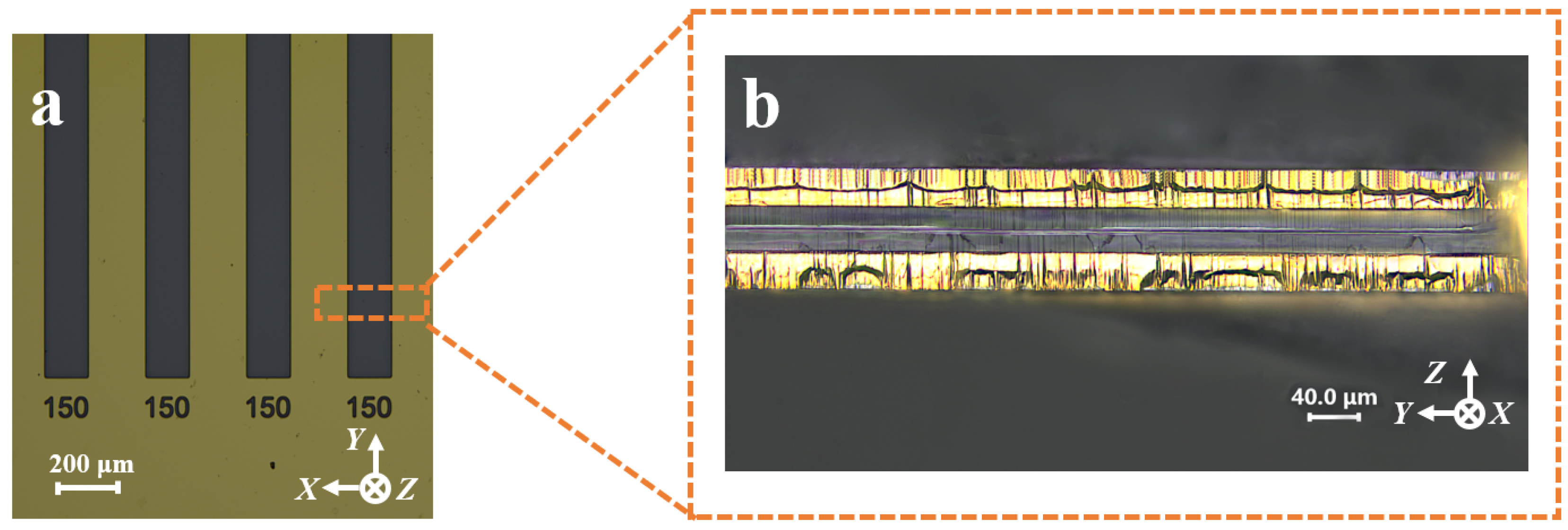
To verify the feasibility of the QMEMS adaptive 3D mask sidewall electrode fabrication process and to enhance its value for practical engineering applications, sidewall discrete electrodes were fabricated within an etching groove with an initial hard mask width of 150 μm following the process flow outlined in
Figure 6. The sample preparation and etching procedures are detailed in
Section 2. The results of the etching process are presented in
Figure 7. It was evident that 3D sidewall discrete electrodes were successfully fabricated within such fine etched grooves. To further confirm the effectiveness of the proposed strategy, the continuity between the two sidewall electrodes was tested using a probe station and a multimeter. The measurement results demonstrated that the two sidewall electrodes were electrically isolated, thereby validating the feasibility of the adaptive 3D mask process.
3.2. Adaptive and Predictable Fabrication of 3D Sidewall Electrodes
The dimensional characteristics of 3D sidewall electrodes have a critical impact on the performance of quartz-based devices. Conventional fabrication methods employing shadow masks are unable to achieve precise and adaptive control of electrode dimensions. In contrast, the self-masking fabrication strategy enables the realization of sidewall electrodes with adaptive and predictable dimensions, as the final electrode size can be accurately tuned based on the etching depth during the initial process step.
However, due to the size effect in the wet etching of quartz crystal [
19,
20], different initial hard mask widths result in varying etch depths. As shown in
Figure 8a, it is evident that a wider initial hard mask leads to a deeper etching depth with the same etching time. At 90 min, the difference in etch depth exceeded 20 μm. In addition, this size effect also significantly influenced the etching morphology.
Figure 8b illustrates the variation in the
P2 platform disappearance time with respect to different initial metal mask widths. It can be observed that the disappearance time of the
P2 plane increased almost linearly with the initial mask width. Specifically, the
P2 disappearance time of a 130 μm mask was nearly 80 min longer than that of a 10 μm mask. These factors collectively impact the final morphology of the sidewall electrodes.
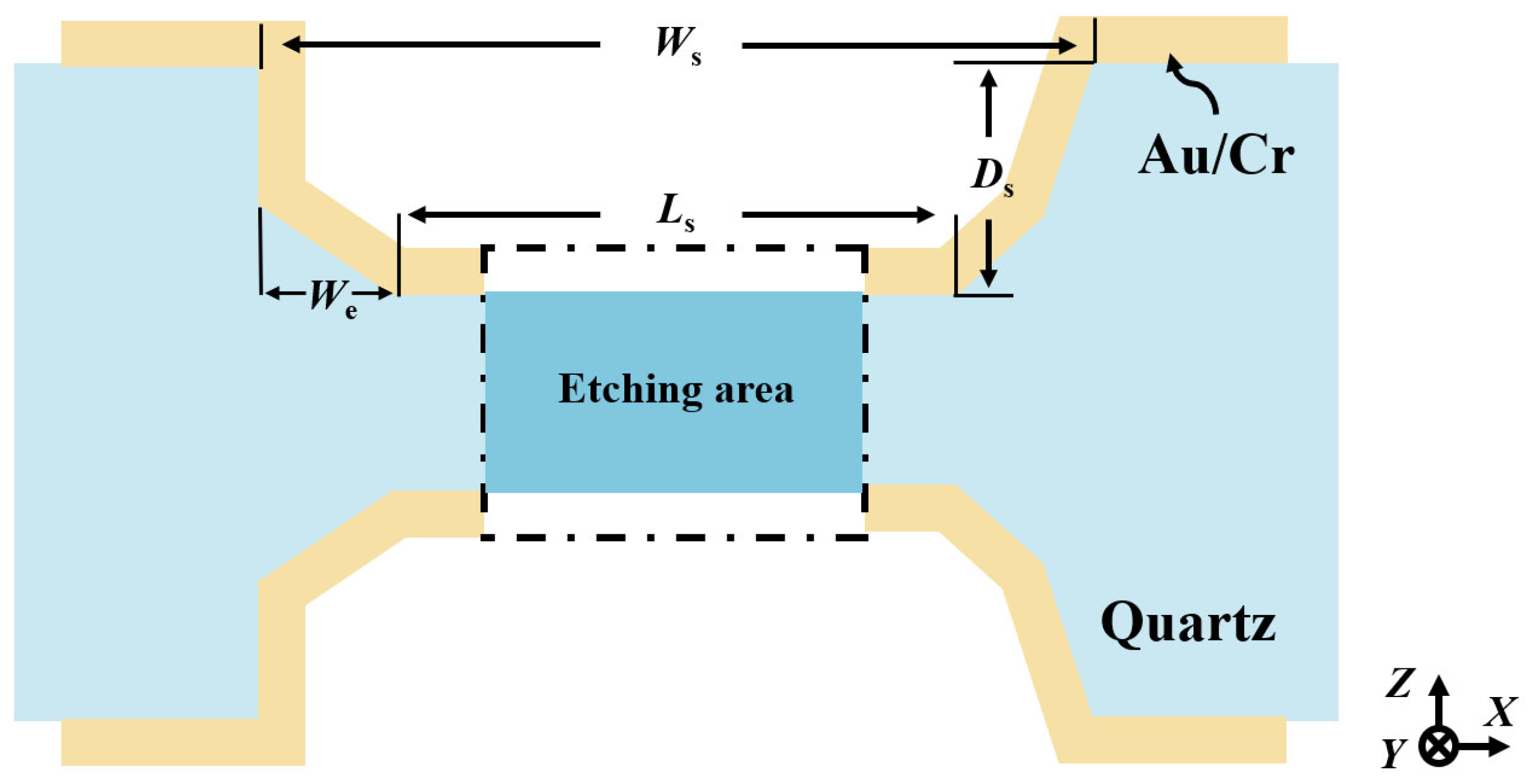
Therefore, to realize an adaptive self-masking fabrication strategy, it is crucial to establish a predicative mathematical model based on extensive etching data analysis. To facilitate this analysis, a simplified schematic of the etched cross-section is provided in
Figure 9. Here,
denotes the etching groove width,
represents the etching depth and the effective width of the sidewall electrodes, and
corresponds to the length of the self-masking beam.
Based on the cross-sectional definition, the actual etching depth
can be equated to the effective electrode width of the sidewall electrodes. Therefore, according to the size effect, the effective width
is jointly determined by the initial hard mask width
and the etching time
. To predict the fabrication dimensions of the sidewall electrodes,
is defined in this work as a function of
and
, as expressed in Equation (1):
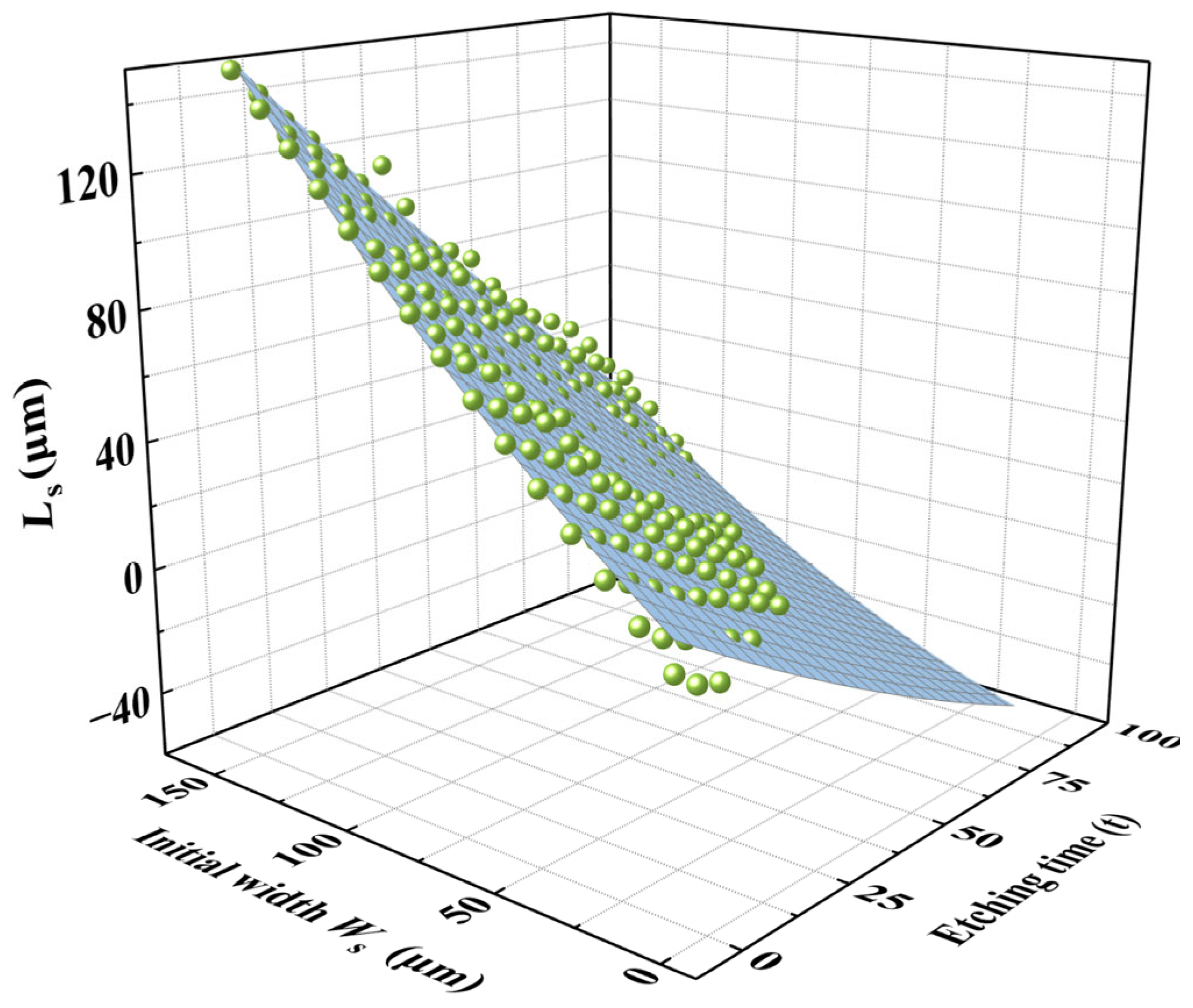
The etching results of initial hard mask widths ranging from 10 μm to 150 μm were plotted into a three-dimensional coordinate system, as shown in
Figure 10.
It was evident that is influenced by both the etching time and the initial hard mask width. Particularly for small initial hard mask widths, the growth of slowed down markedly with increasing etching time due to the pronounced size effect. In contrast, the impact of size effect on is less significant.
The relationship of
was obtained by fitting the experimental data using a binary quadratic (Poly2D) function, leading to the effective width prediction model shown in Equation (2):
where the
x is the etching groove width
and
y means the etching time
.
The experimental data were substituted in Equation (2) for fitting, and the resulting coefficients along with their coefficients of determination (
) are summarized in
Table 1.
The table shows that the coefficient of determination, , was as high as 0.994, indicting a strong fit of the coefficients. The fitting function accurately represents the change of etching depth under the combined influence of initial hard mask width and etching time. Based on this equation, it is possible to predict the effective electrode width, , at any etching time for any initial hard mask width, enabling precise control over the 3D sidewall discrete electrodes.
3.3. Fabrication of 3D Sidewall Electrodes in Ultrafine Etching Grooves
In this section, the process limitations of the adaptive 3D self-masking fabrication strategy are discussed.
For practical application, to ensure both feasibility and repeatability, the self-masking beam length was selected as the lithographic hard mask pattern width for secondary lithography. Due to size effects, the etching platform width is jointly influenced by the initial hard mask width and the etching time t.
Therefore,
can be defined as a binary function of
and
t, as expressed in Equation (3):
The etching results for initial hard mask widths ranging from 10 μm to 150 μm were plotted in a 3D coordinate system, as shown in
Figure 11.
Similarly, the size effect on was negligible when the etching time was short or when the initial hard mask width was relatively large. However, for smaller initial hard mask widths combined with longer etching times, the size effect on became increasingly significant.
Since
is also a binary function of the initial hard mask width and etching time, an empirical relationship can be established by fitting the experimental data using a binary quadratic (Poly2D) function. Thus,
could be expressed as shown in Equation (4):
where the
x is the etching platform width
and
y means the etching time
.
The experimental data were substituted in Equation (4) and fitted accordingly. The resulting coefficients, along with their corresponding coefficients of determination (
), are summarized in
Table 2.
The data in
Table 2 show that the coefficient of determination
R2 reached 0.989, demonstrating a strong fit of the coefficients.
To ensure that the sidewall discrete electrodes remain electrically isolated, it is necessary to maintain the presence of the etching self-masking beam even when the etching groove reaches approximately half of the wafer thickness.
In practice, extending the secondary etching time can flatten the sidewall rise, thereby improving device performance [
21]. However, excessive etching may cause discrete electrodes to short-circuit. Thus, a certain degree of design redundancy must be incorporated into the process to prevent the sidewall from leading to electrode short-circuiting, thereby enhancing the stability and reproducibility of the technology.
To avoid electrode short-circuiting, it is essential to satisfy the conditions shown in Equation (5), as illustrated in
Figure 12:
where
is the wafer thickness and
is the angle between the etched crystal plane and the Z-direction.
In this work, = 120 μm, = 61°, yielding a maximum allowable of 52.4 μm. For simplicity in subsequent calculations, was set to 52 μm.
In summary,
must satisfy the condition expressed in Equation (6):
where
is the etching time when
. This can be expressed as follows, according to Equation (7):
Thus, for
, we have the following:
To determine the thinnest initial hard width,
, that can be manufactured under this condition,
must satisfy Equation (9):
Substituting the coefficients obtained from
Table 2 into the
function, the expression for
is as follows:
For the
-term coefficients, given that
and
we can neglect the terms
and
.
Similarly, for
y-term coefficients,
so we can disregard
.
Thus,
could be simplified as follows:
Substituting the coefficients into the
function, we obtain
Now,
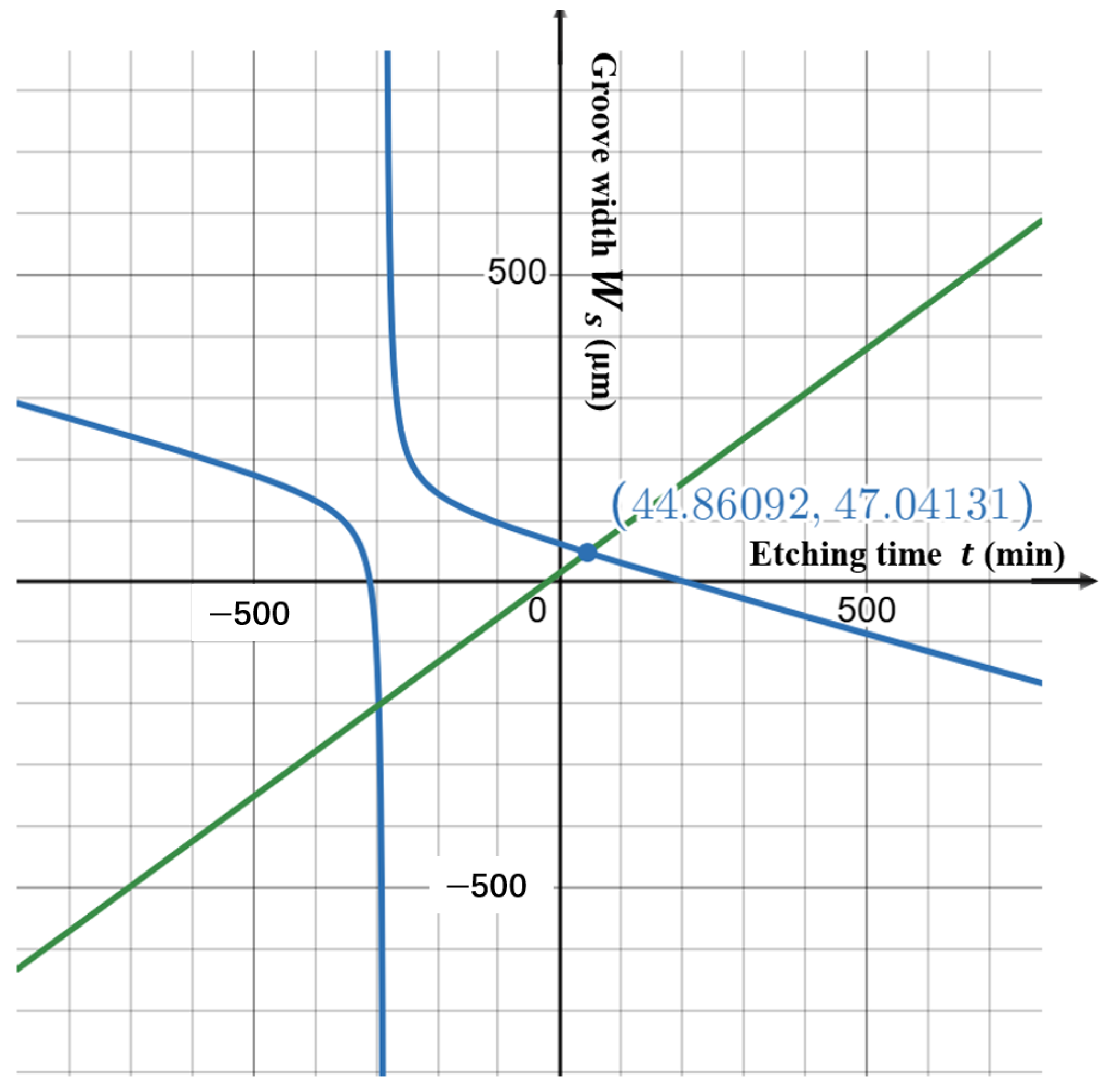
can be calculated as follows:
Setting
, the following equation can be solved:
The graph of the above equation is shown in
Figure 13. By using the graphical solutions, the minimum initial hard mask width
was determined for this process condition.
To validate the theoretical calculations, sidewall discrete electrodes were fabricated using the 3D adaptive self-masking micro-fabrication strategy in a deep etching groove with an initial hard mask width of 45 μm. The fabrication results are shown in
Figure 14. It is evident that 3D sidewall electrodes were successfully formed on both the +X side (
Figure 14b) and the −X side (
Figure 14c). This strategy enables the fabrication of 3D sidewall electrodes within ultrafine etching grooves, providing a pathway toward the extreme miniaturization of QMEMS out-of-plane vibration units.
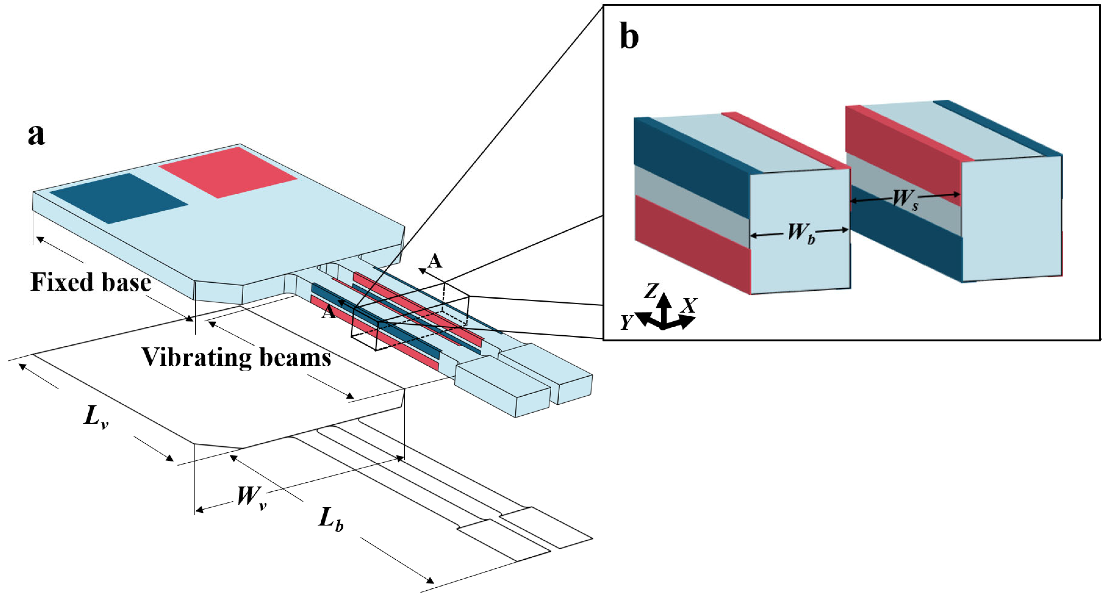
3.4. Fabrication of Ultra-Small Vibration Unit Based on Self-Masking Fabrication Strategy
The self-masking etching strategy was employed to fabricate an ultra-small out-of-plane vibration unit on a 120 μm thick quartz wafer.
Figure 15 illustrates the structure and key dimensions of the unit. The vibration unit consists of vibration beams and a supporting base. Each vibration beam has a length of 2000 μm and a width of 175 μm, and the gap between two adjacent beams
is only 150 μm. The key dimensional parameters of the unit are summarized in
Table 3.
The vibration unit was fabricated by using the self-masking strategy.
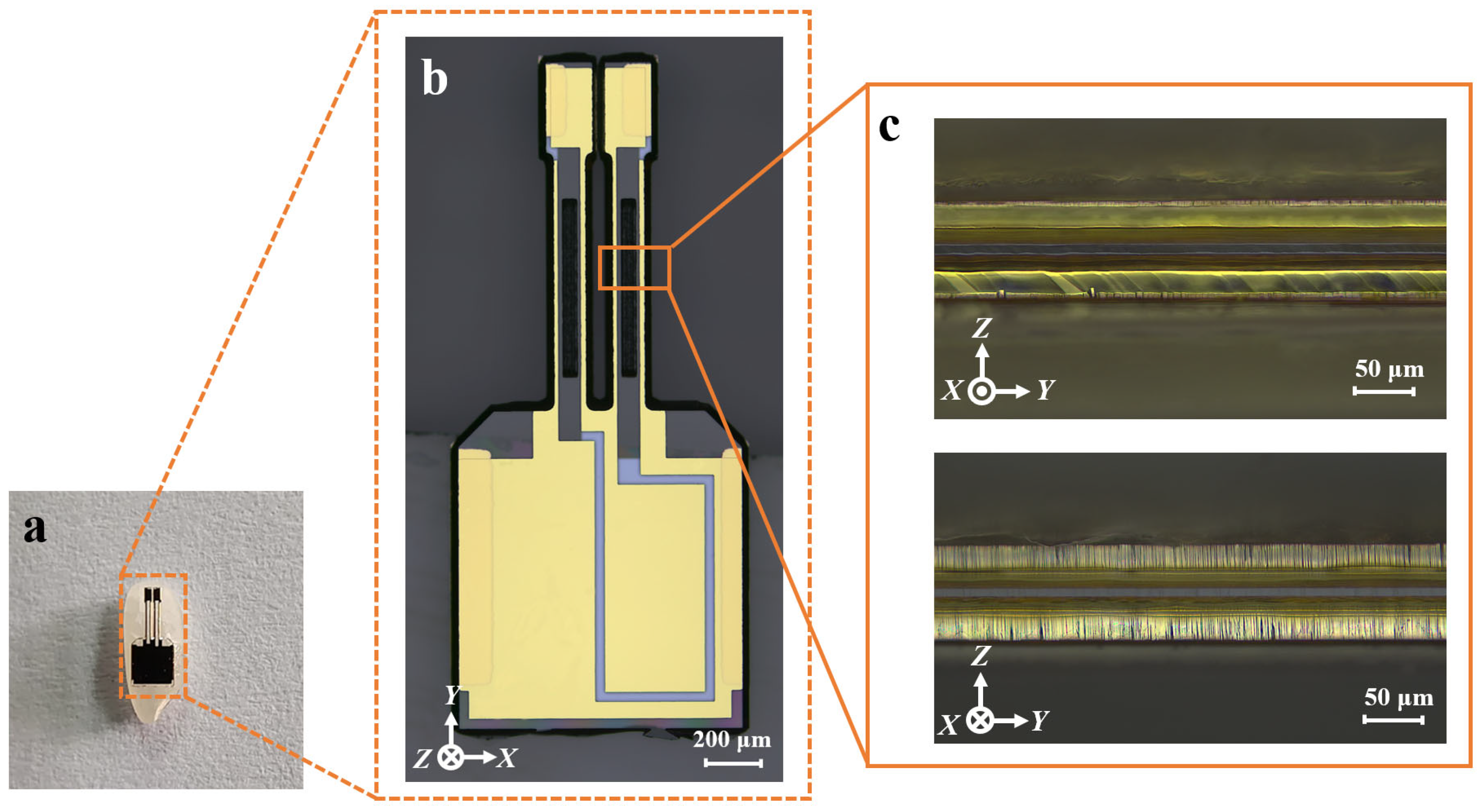
Figure 16 presents a cross-sectional view of the completed vibrating unit and its vibrating beam. To provide a sense of scale, the unit is shown placed on a grain of rice (
Figure 16a). As seen from the cross-section image (
Figure 16c), the sidewalls exhibit uniform discrete electrodes.
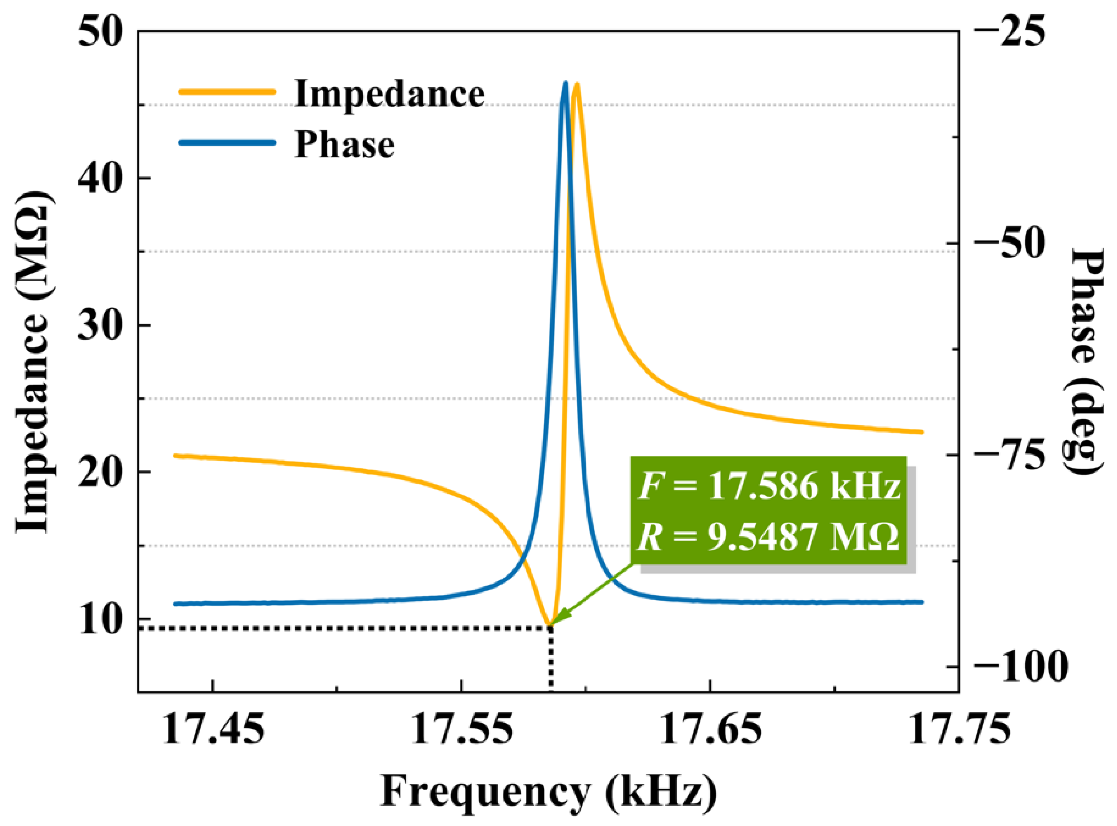
The vibration unit was tested using an impedance analyzer at normal atmospheric pressure, and the test results are shown in
Figure 17. The resonant frequency was measured at 17.58 kHz, with a resonant impedance of 9.55 MΩ, both of which align with the design specifications.
In this study, five units were fabricated and tested. The statistical results are presented in
Table 4. The repeatability error is defined as follows:
where
is the standard deviation of multiple measurements, and
is the absolute value of the average of multiple measurements.
The repeatability errors in a wafer were also tested, as presented in
Table 5.
As shown in the table, the process repeatability errors for the critical dimensions of the device were all within 1.13% and the repeatability errors in a wafer were all within 0.74%, demonstrating that the innovative fabrication method proposed in this paper exhibits excellent repeatability. This indicates that the self-masking fabrication strategy holds significant potential for large-scale mass production.


