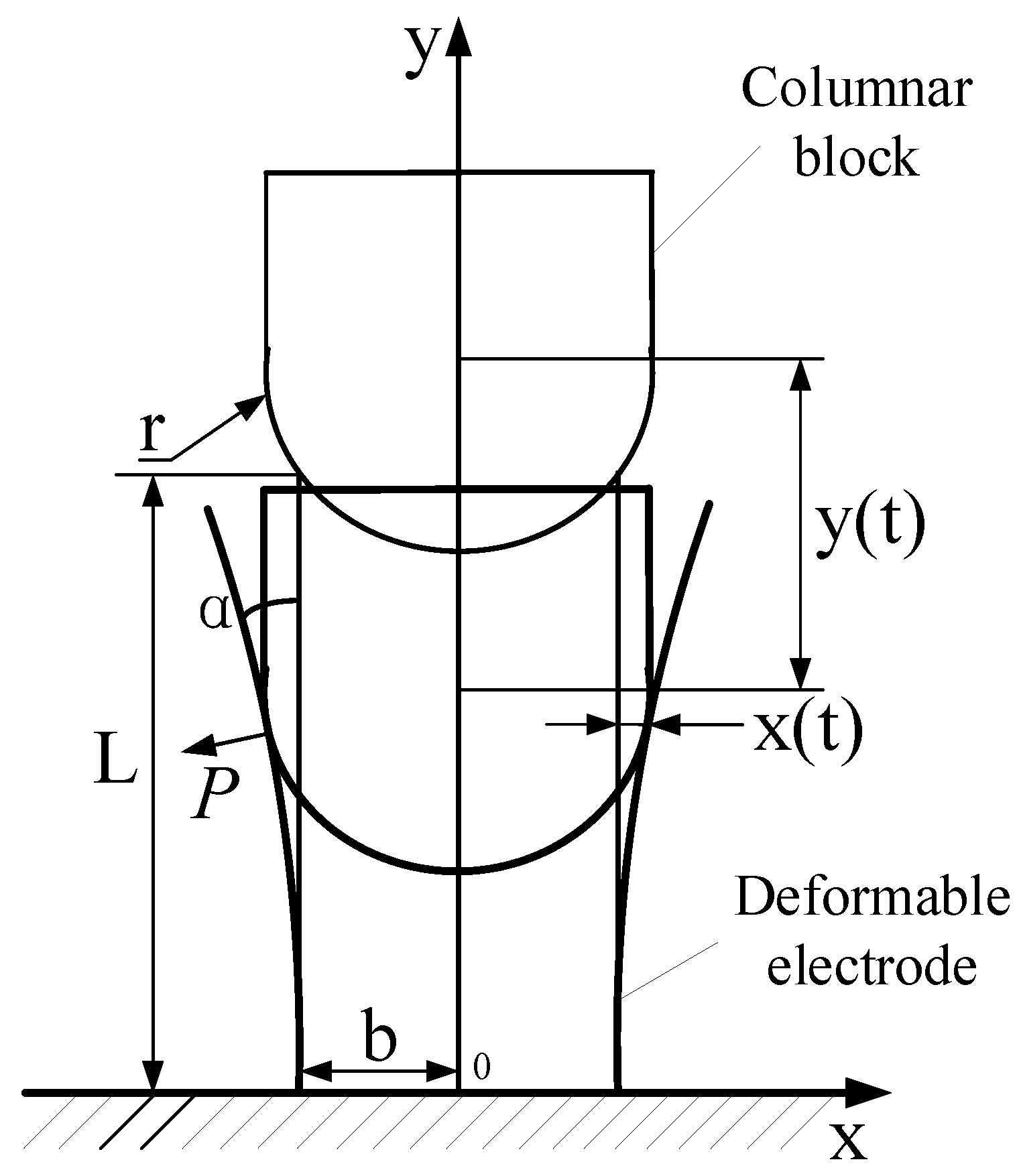
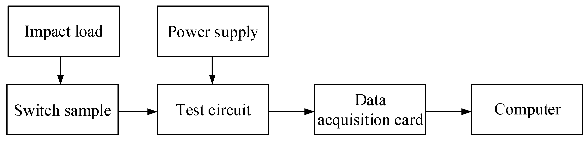
3.2. Best Parameter Combination Scheme
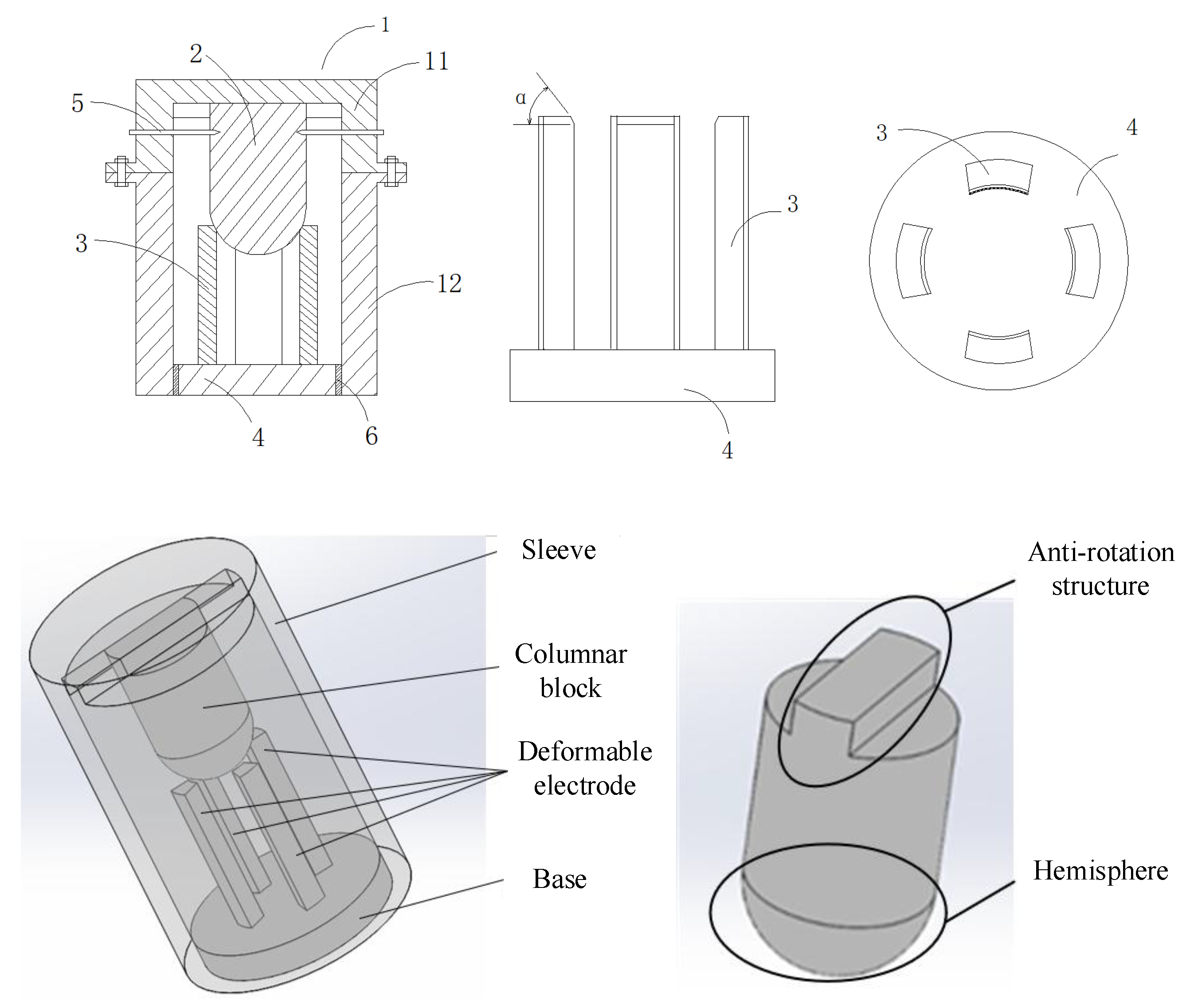
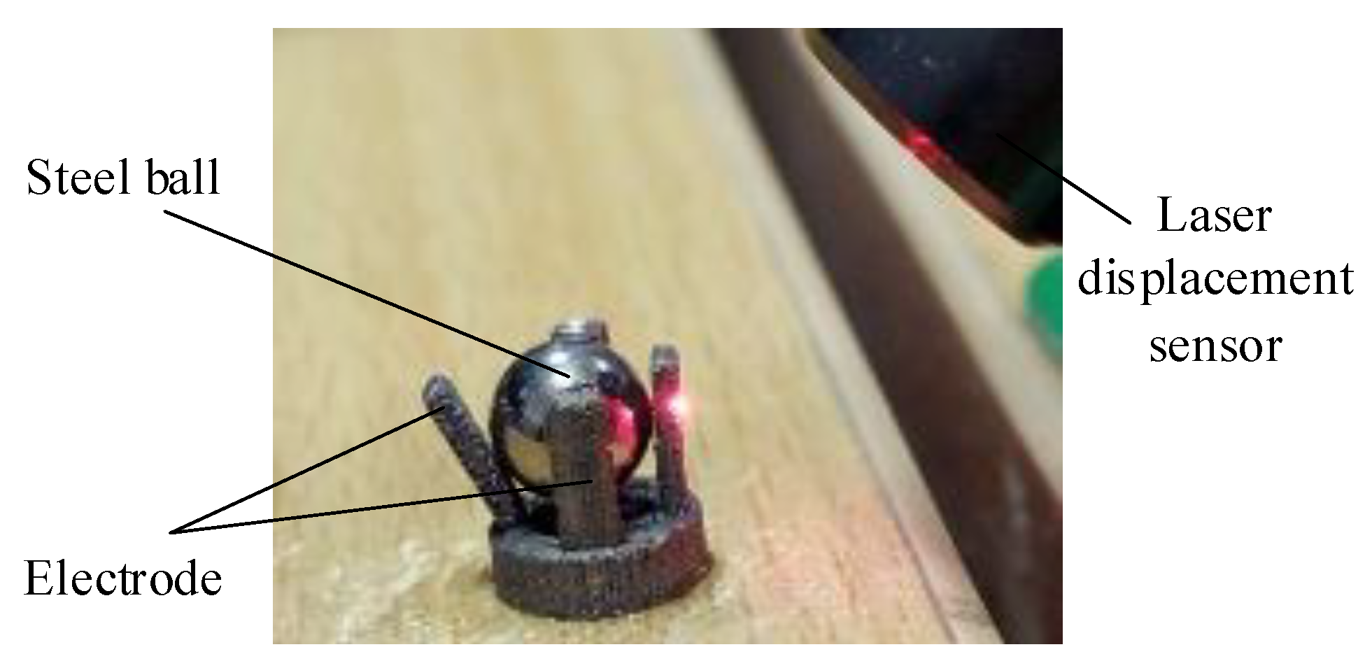
In order to reduce the calculation time of finite element simulation, the columnar block is treated as a rigid body and divided into tetrahedral meshes. The remaining parts of the switch are divided into hexahedral meshes with a higher calculation accuracy. The aluminum alloy electrodes were used in the simulation. The contact area between the electrode and the outer sleeve was used as the assessment result of the orthogonal experimental simulation.
According to the parameter arrangement in
Table 1 and
Table 2, professional finite element simulation software ABAQUS (version 5.4) was used for the simulation calculations, and the orthogonal experimental simulation results of four factors and three levels were obtained, as shown in
Table 3.
In
Table 3,
is the sum of the experimental results corresponding to level
i in each column.
is calculated as
where
m is the number of experiments at level
i in each column; here
.
Range R is the maximum minus the minimum of k values in each column. The magnitude of R value can be used as an indicator to determine the influence of various factors on the experimental results. The larger the R value, the greater the impact of this factor on the experimental results. The R value of each factor should be greater than that of the blank column. Obviously, the R values of factors A, B, and C are all greater than the R value of the blank column, indicating that factors A, B, and C are the main factors. And means that factor A (hemisphere diameter) has the greatest impact on the experimental results, followed by factor B (electrode width), and the least is factor C (electrode thickness).
Based on the orthogonal experimental simulation results, the parameters of the electrode are further determined through variance analysis. According to the basic principle of variance analysis, we calculate total sum of squared deviations as follows:
The total sum of squared deviations is the sum of the squared deviations of all data from their total mean, reflecting the overall fluctuation of experimental results, which is caused by changes in factor levels and experimental errors.
The column sum of squared deviations is calculated as follows:
reflects the fluctuation of experimental results caused by changes in the level of factors in this column. If the column is a blank column, then represents the fluctuations caused by experimental errors and unobserved factors. In the variance analysis of the orthogonal experiment, the sum of squared deviations of the blank column is usually regarded as the sum of squared deviations of experimental errors, and it is used for significance testing.
The total degree of freedom is . The degree of freedom for the factor in column j is .
Calculate variance based on the definition of variance, construct F-statistic, create variance analysis table, and perform significance test. The results are shown in
Table 4.
From the results of the variance analysis, it can be seen that factor A (hemisphere diameter) has a highly significant impact, factor B (electrode width) has a significant impact, and factor C (electrode thickness) has no significant impact. The results of this analysis are the same as those in the range analysis.
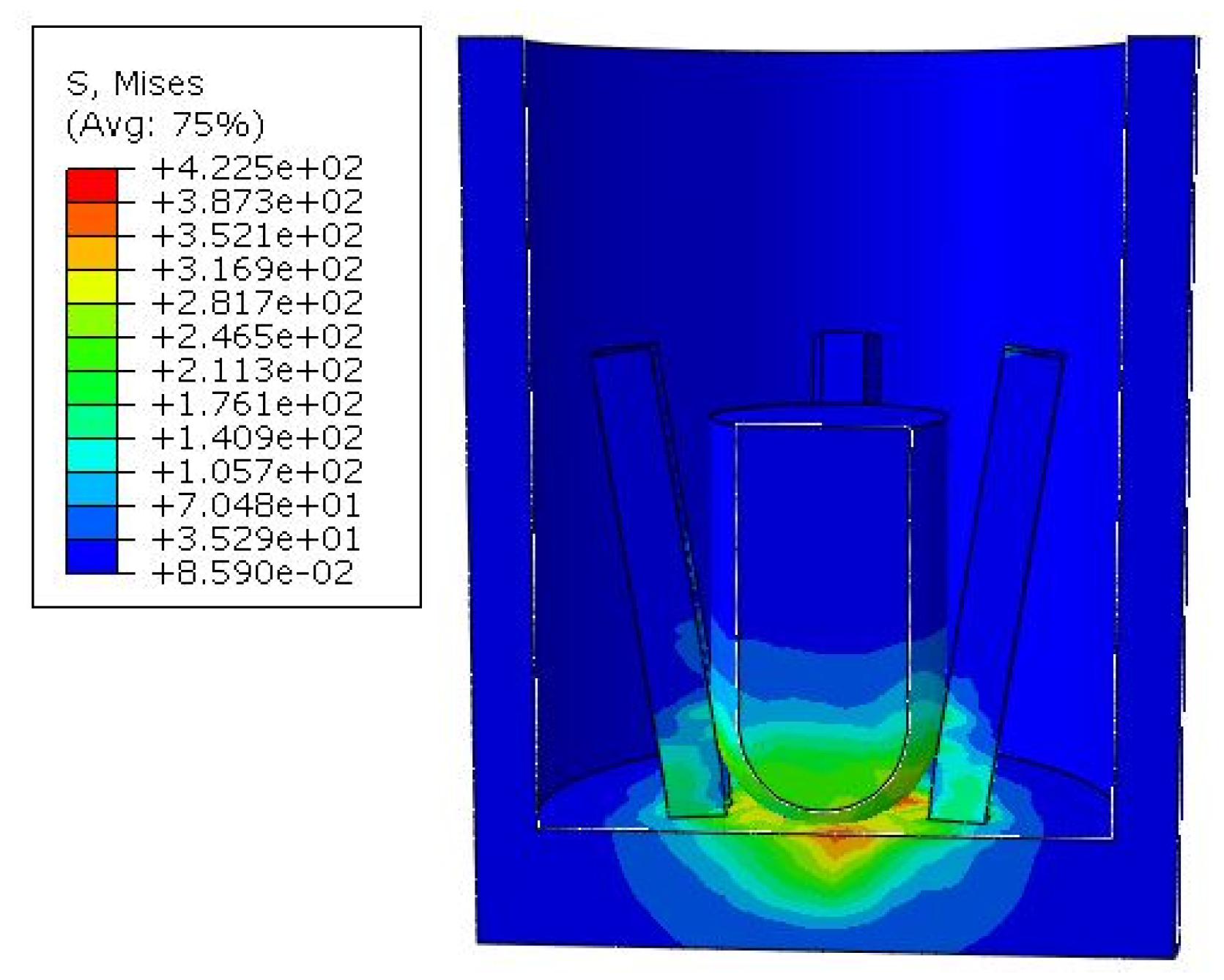
There are two main types that greatly affect the closing performance of the electrode. One type is completely non-contact, and the main reason for this result is that the diameter of the hemisphere is too small to fully extend the electrode. The simulation result is shown in
Figure 9.
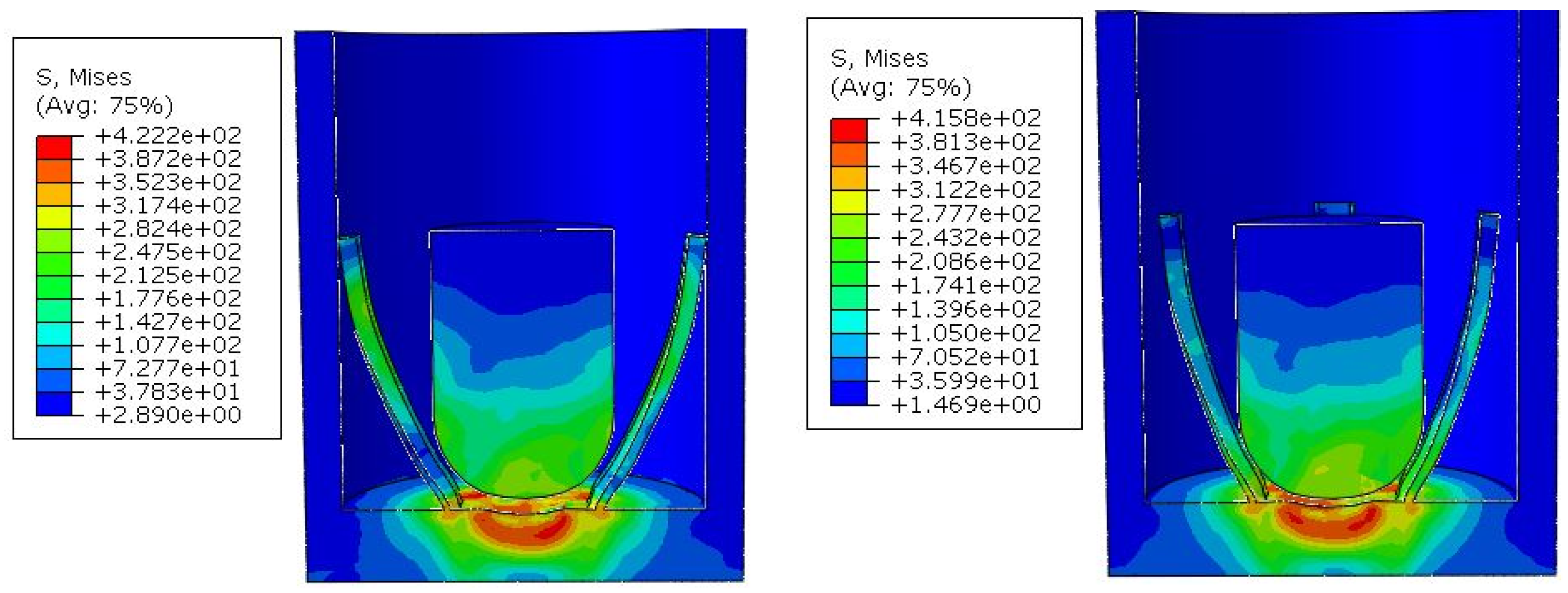
Another type is caused by the large diameter of the hemisphere. When the columnar block reaches the bottom, it squeezes the root of the electrode, causing the top to warp. During the entire force process, the electrode and the outer sleeve make intermittent contact, causing unstable power connection, which seriously affects the performance of the switch.
Figure 10 shows the simulation results of the
scheme.
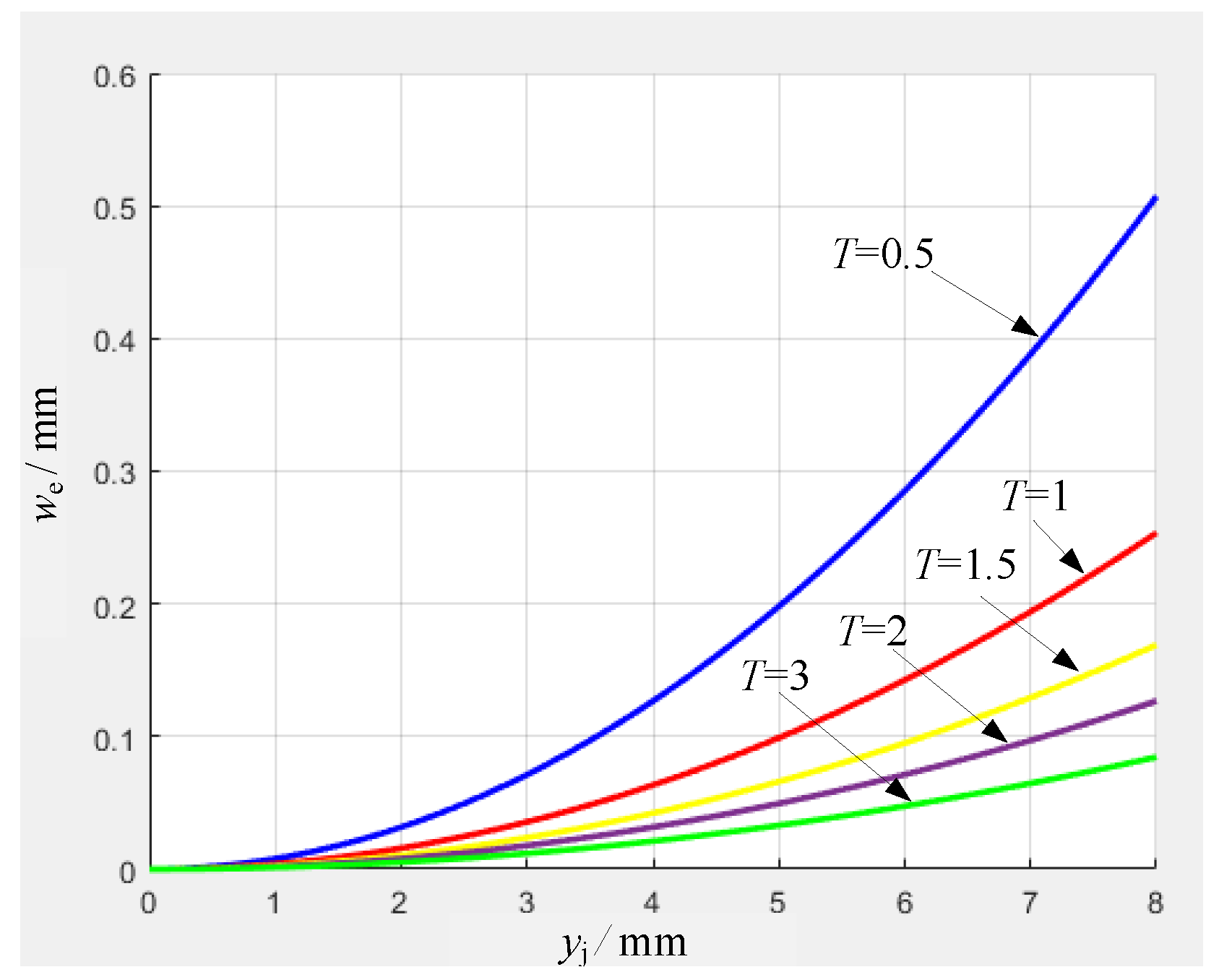
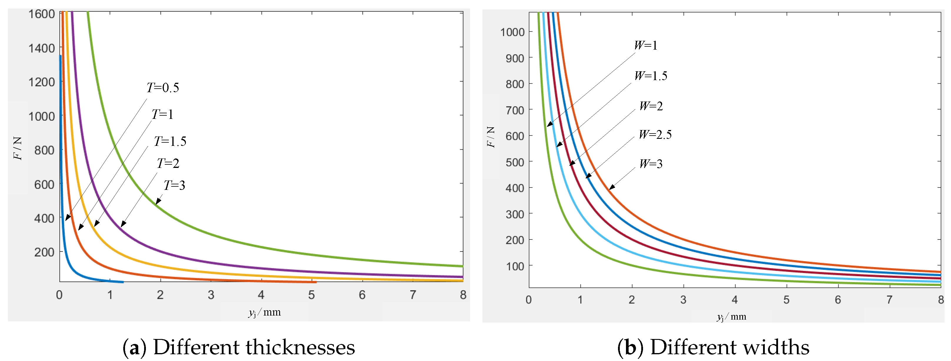
Simulation results indicate that in the case of the same width-to-thickness ratio of the electrode, the larger the hemisphere diameter, the larger the contact area. In the case of a larger width-to-thickness ratio, although the outer surface area of the electrode increases, it is very easy to cause the electrode to warp, causing severe shaking in the deformation process and affecting the stability of the switch. Therefore, it is not advisable to choose a larger width-to-thickness ratio in the switch design process, and the hemisphere diameter can be chosen to be larger within the allowable range.
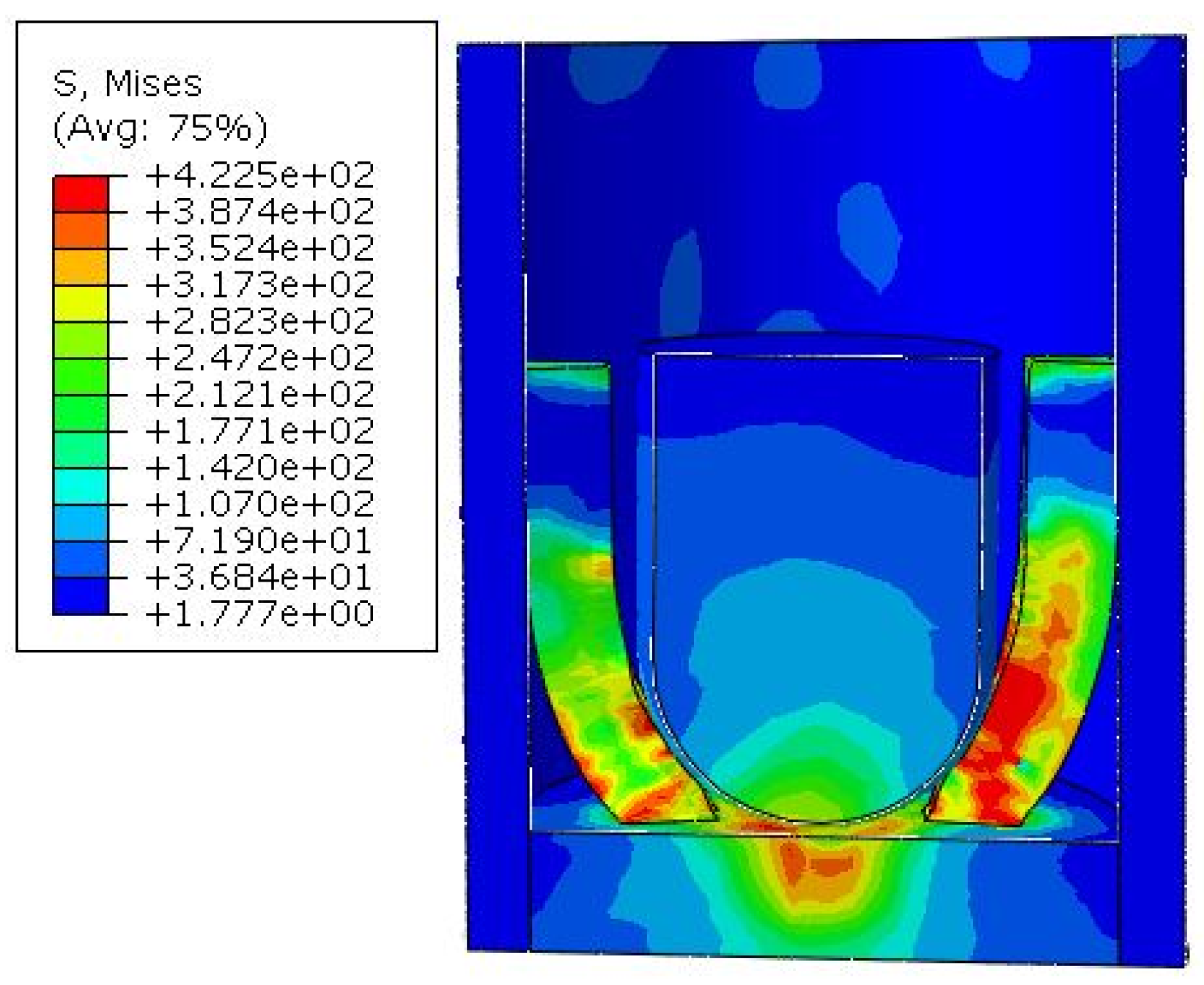
According to the
values of various factors in the orthogonal experimental simulation results, the diameter of the hemisphere is selected as level 2, the electrode width is selected as level 3, and the electrode thickness is selected as level 2, that is, the
scheme. It is considered that this scheme is the best parameter combination scheme. The simulation result is shown in
Figure 11.
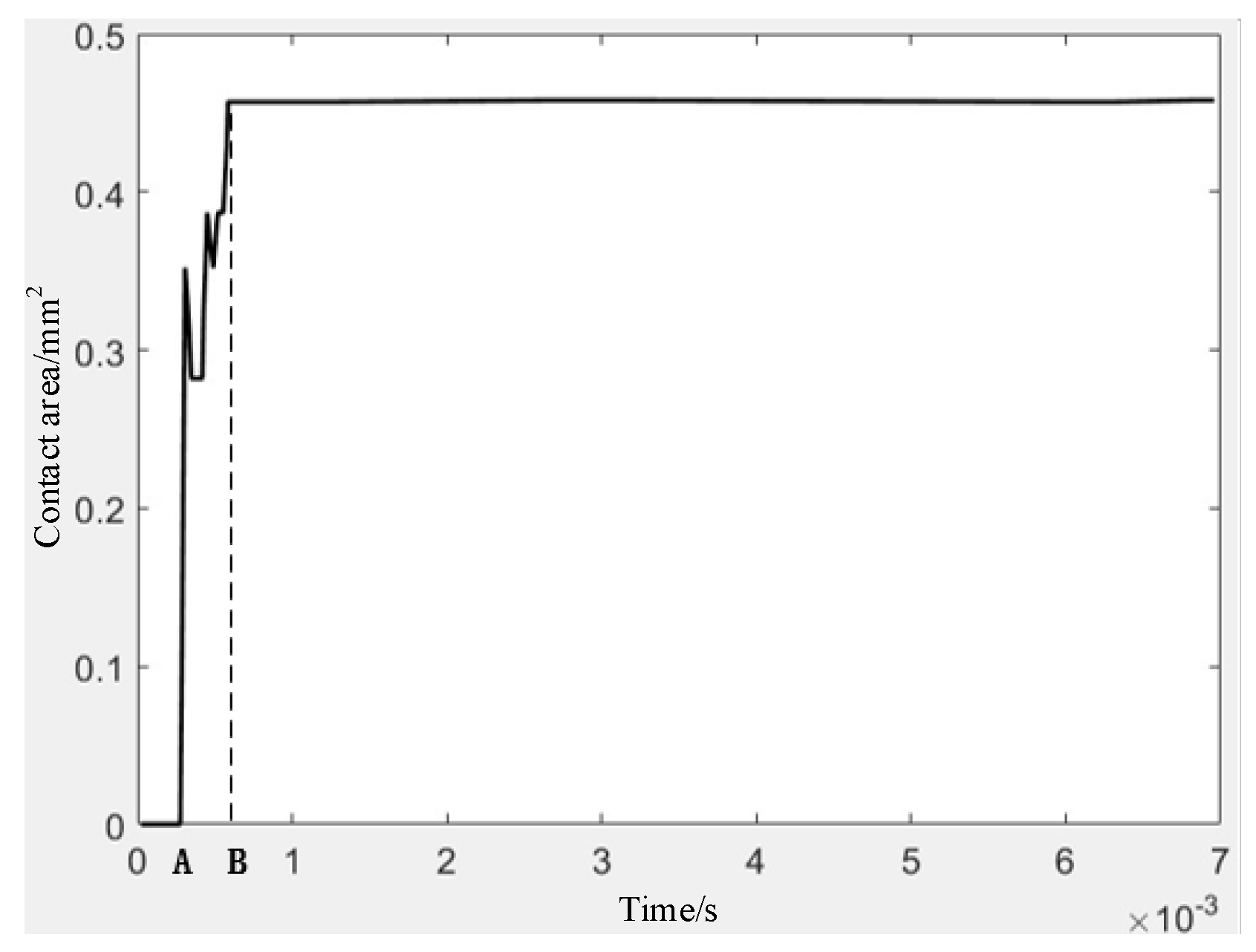
From the simulation result, it can be seen that the electrode has undergone plastic deformation and is tightly in contact with the outer sleeve. The contact curve is shown in
Figure 12. After a very short period of shaking, the contact between the electrode and the outer sleeve is stable, and the contact area is larger than that of nine simulations in the orthogonal experiment. The total contact area of the four electrodes is 1.8
.
In summary, the hemisphere diameter, electrode width, and electrode thickness all have an impact on the electrode contact performance. Among them, the hemisphere diameter has the greatest impact, followed by the electrode width, and the least is the electrode thickness.
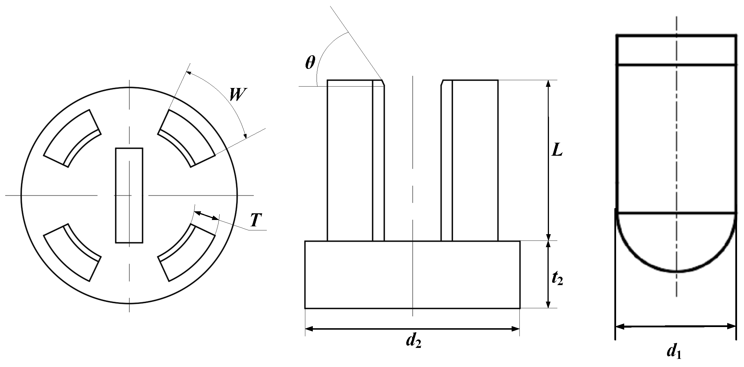
The best parameter combination scheme for the electrode is the scheme, that is, the hemisphere diameter mm, the electrode width mm, and the electrode thickness mm.


