Article

Optimization of Low-Voltage p-GaN Gate HEMTs for High-Efficiency Secondary Power Conversion

by
Lili Zhai
1,
Xiangdong Li
1,2,*,
Jian Ji
1,
Lu Yu
1,
Liang Chen
1,
Yaoming Chen
1,
Haonan Xia
1,
Zhanfei Han
1,
Junbo Wang
1,
Xi Jiang
1,2,
Song Yuan
1,2,
Tao Zhang
1,2,
Yue Hao
1,2 and
Jincheng Zhang
1,2,*
1
Guangzhou Wide Bandgap Semiconductor Innovation Center, Guangzhou Institute of Technology, Xidian University, Guangzhou 510555, China
2
State Key Laboratory of Wide Bandgap Semiconductor Devices and Integrated Technology, School of Microelectronics, Xidian University, Xi’an 710071, China
*
Authors to whom correspondence should be addressed.
Micromachines 2025, 16(5), 556; https://doi.org/10.3390/mi16050556
Submission received: 2 April 2025 / Revised: 29 April 2025 / Accepted: 1 May 2025 / Published: 2 May 2025
(This article belongs to the Section E:Engineering and Technology)

Abstract

:
The explosive demand for high-performance secondary power sources in artificial intelligence (AI) has brought significant opportunities for low-voltage GaN devices. This paper focuses on research on high-efficiency and high-reliability low-voltage p-GaN gate HEMTs with a gate–drain distance, LGD, of 1 to 3 μm in our pilot line, manufactured on 6-inch Si using a CMOS-compatible process, with extraordinary wafer-level uniformity. Specifically, these fabricated p-GaN gate HEMTs with an LGD of 1.5 μm demonstrate a blocking voltage of over 180 V and a high VTH of 1.6 V and exhibit a low RON of 2.8 Ω·mm. It is found that device structure optimization can significantly enhance device reliability. That is, through the dedicated optimization of source field plate structure and interlayer dielectric (ILD) thickness, the dynamic ON-resistance, RON, degradation of devices with an LGD of 1.5 µm was successfully suppressed from 60% to 20%, and the VTH shift was significantly reduced from 1.1 to 0.5 V. Further, the devices also passed preliminary gate bias stress and high-voltage OFF-state stress tests, providing guidance for preparing high-performance, low-voltage p-GaN gate HEMTs in the future.

1. Introduction

GaN devices are increasingly displacing conventional Si MOSFETs in low-voltage applications, demonstrating superior switching performance while achieving higher power densities [1,2,3,4]. In practical applications, low-voltage p-GaN gate power HEMTs offer significant advantages in fields that require high-frequency switching and fast responses due to their lower switching losses and faster response speeds [5,6]. Since 2024, sub-100 V GaN power HEMTs have found implementation in cutting-edge technological domains including industrial robotics, smart home appliances, next-generation e-mobility solutions, and autonomous unmanned aerial systems [7,8].
Recently, the rapid advancement of artificial intelligence (AI) technologies has created an unprecedented demand for efficient and compact secondary power solutions. This surge in power requirements has catalyzed significant research into low-voltage GaN power devices that are particularly suitable for meeting the stringent power demands of AI systems, ranging from data centers to edge computing devices [9,10,11]. Therefore, more and more low-voltage GaN power devices and related applications have been reported and released to the market, such as a full-bridge LLC DC-DC converter (48 V-5 V) based on p-GaN gate power devices and a monolithic integrated enhancement-mode (e-mode) GaN 48 V-to-1 V DC-DC buck converter [12,13]. EPC has released the commercially available 30 V e-mode GaN power transistor half-bridge of EPC2100 [14]. A low-voltage power device for high-efficiency secondary power conversion must combine high reliability and low RON. However, low-voltage p-GaN gate power HEMTs face several challenges that need to be addressed [15,16,17], particularly concerning the stability and reliability of device performance, depending on device structure, material properties, and operating conditions [18,19]. The optimization of the field plate in GaN HEMTs can effectively modulate the blocking capability and dynamic characteristics, representing a critical factor influencing device performance [20,21]. However, these critical factors are insufficiently researched regarding low-voltage p-GaN gate HEMTs.
In this work, the feasibility of fabricating low-voltage p-GaN gate HEMTs with low RON and high stability on a 6-inch Si substrate will be comprehensively analyzed. An epitaxy- and CMOS-compatible process for low-voltage p-GaN gate power devices in our pilot line will first be introduced. Optimization of field plate structure and the interlayer dielectric (ILD) thickness will then be conducted, and the impact will be deeply assessed using electrical characterizations of yield, gate reliability, dynamic RON, and OFF-state stress so as to provide guidance for fabricating high-performance power devices for AI secondary power systems in the future.

2. Materials and Methods
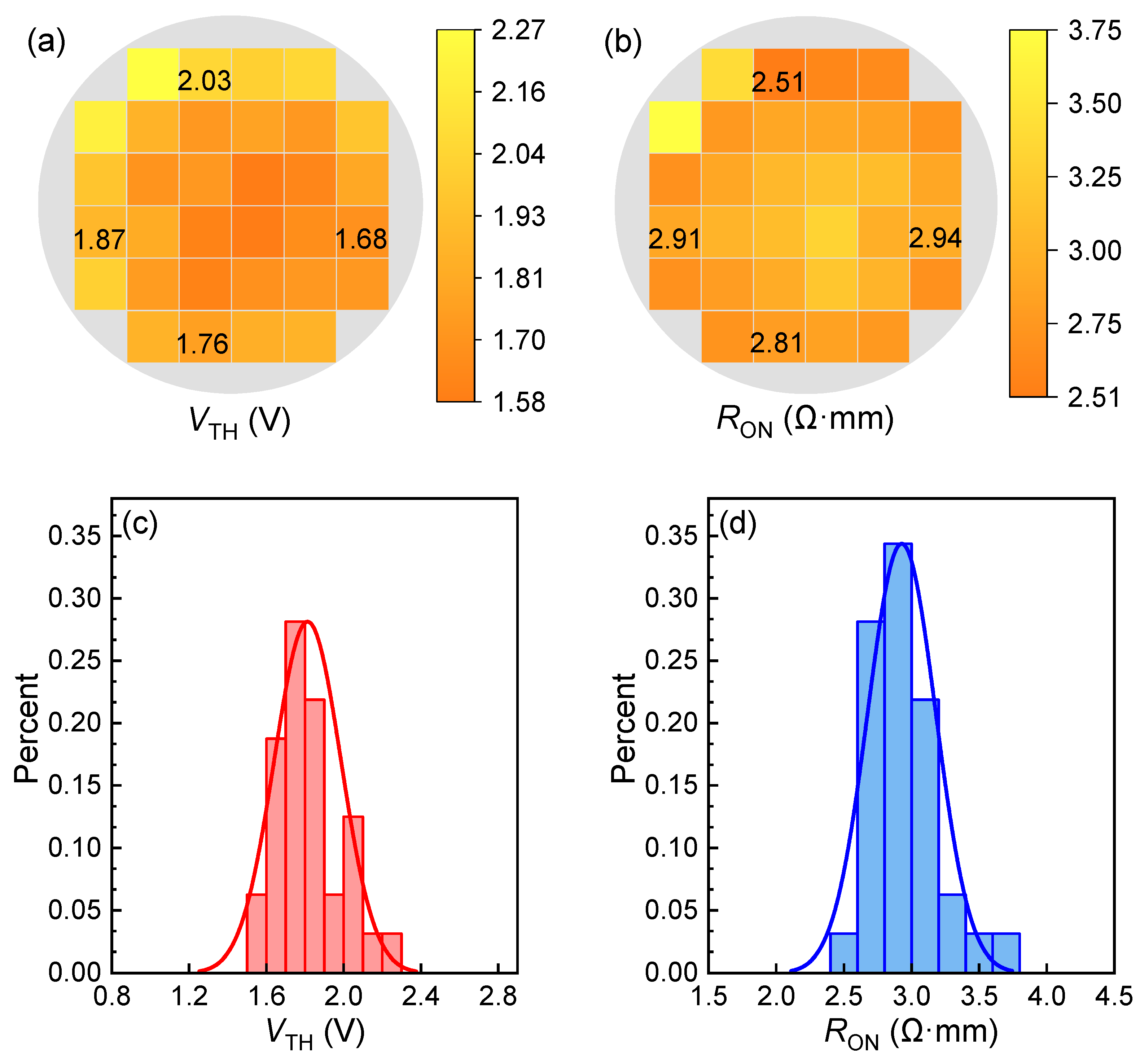
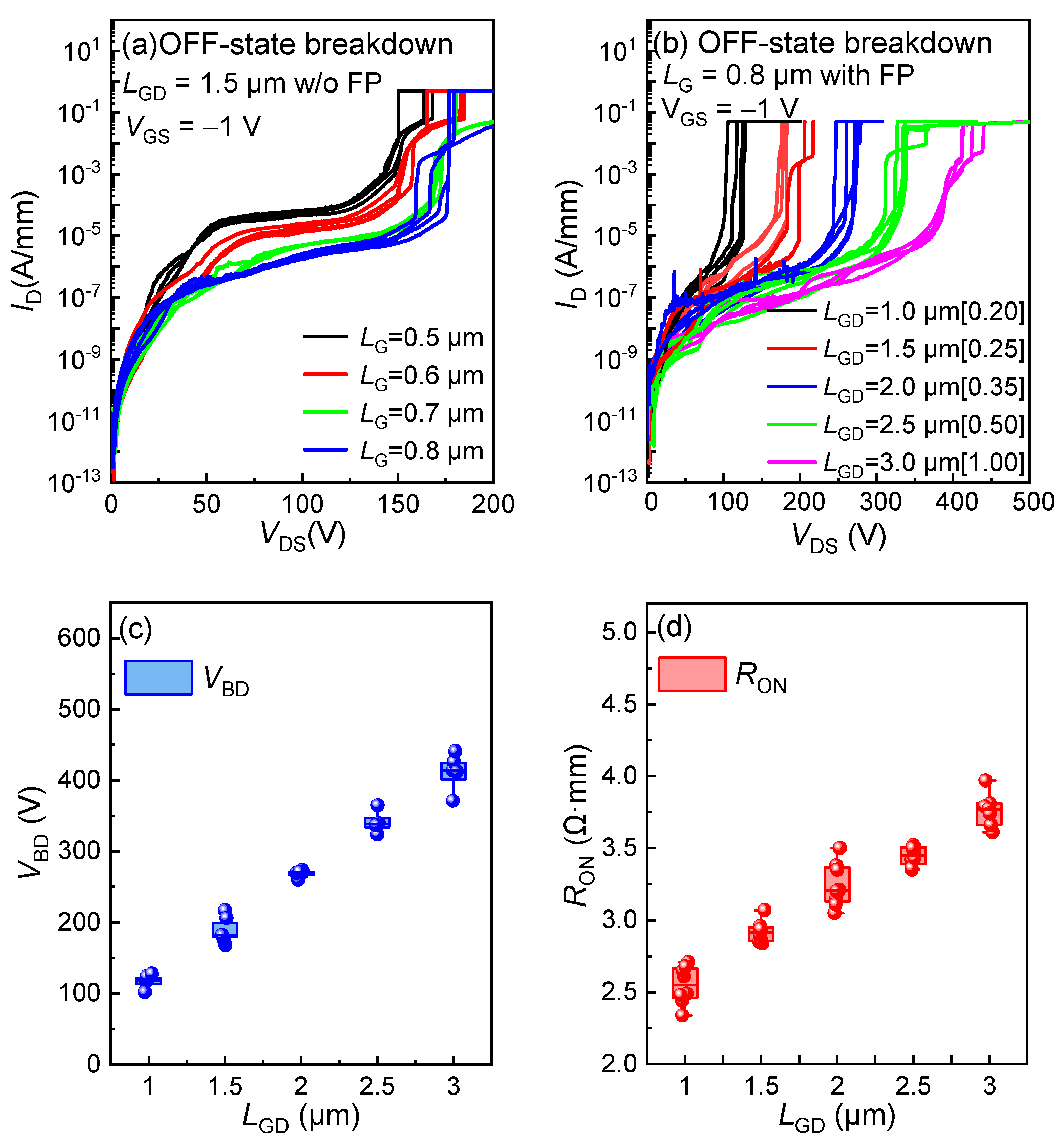
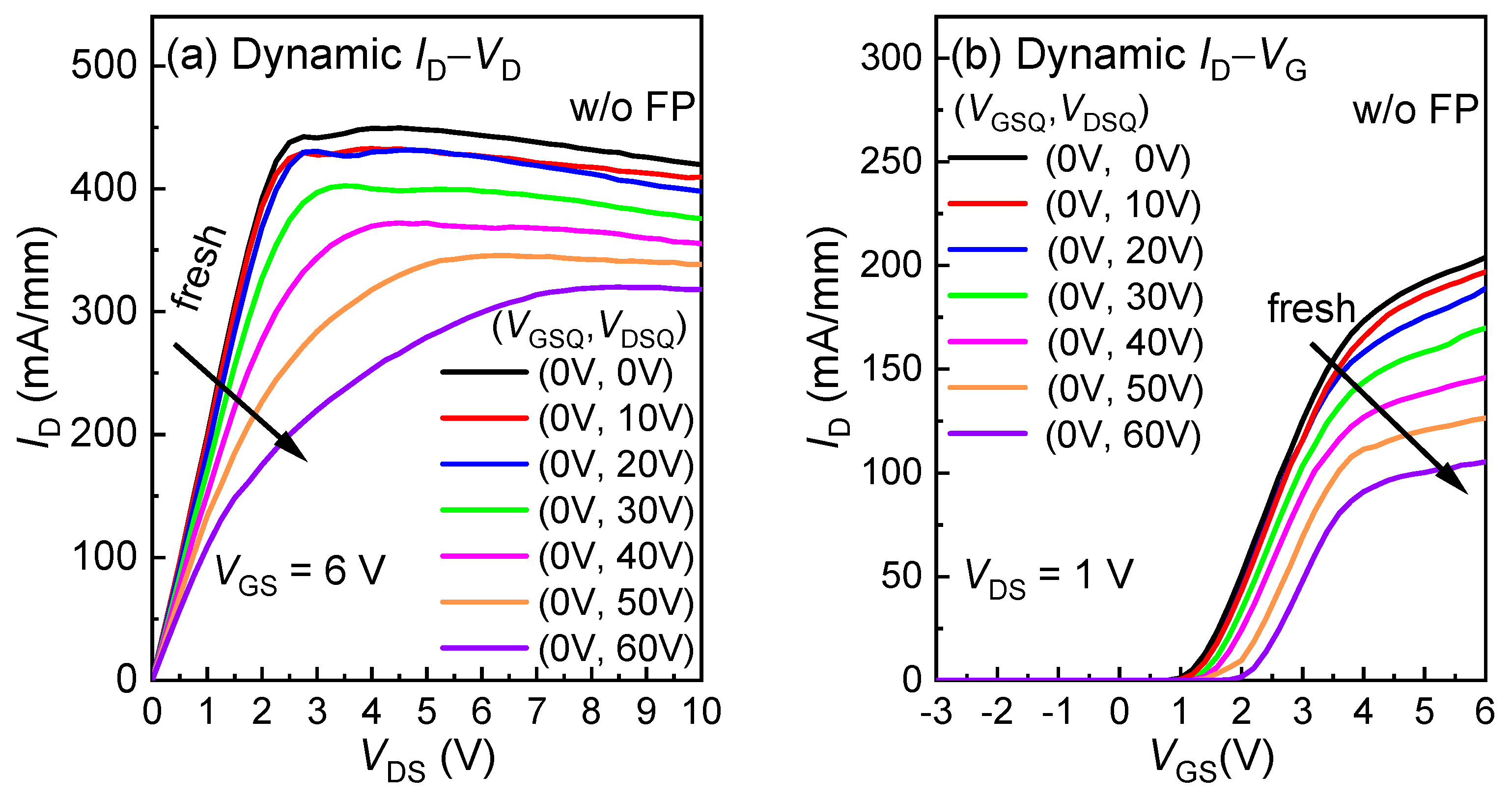
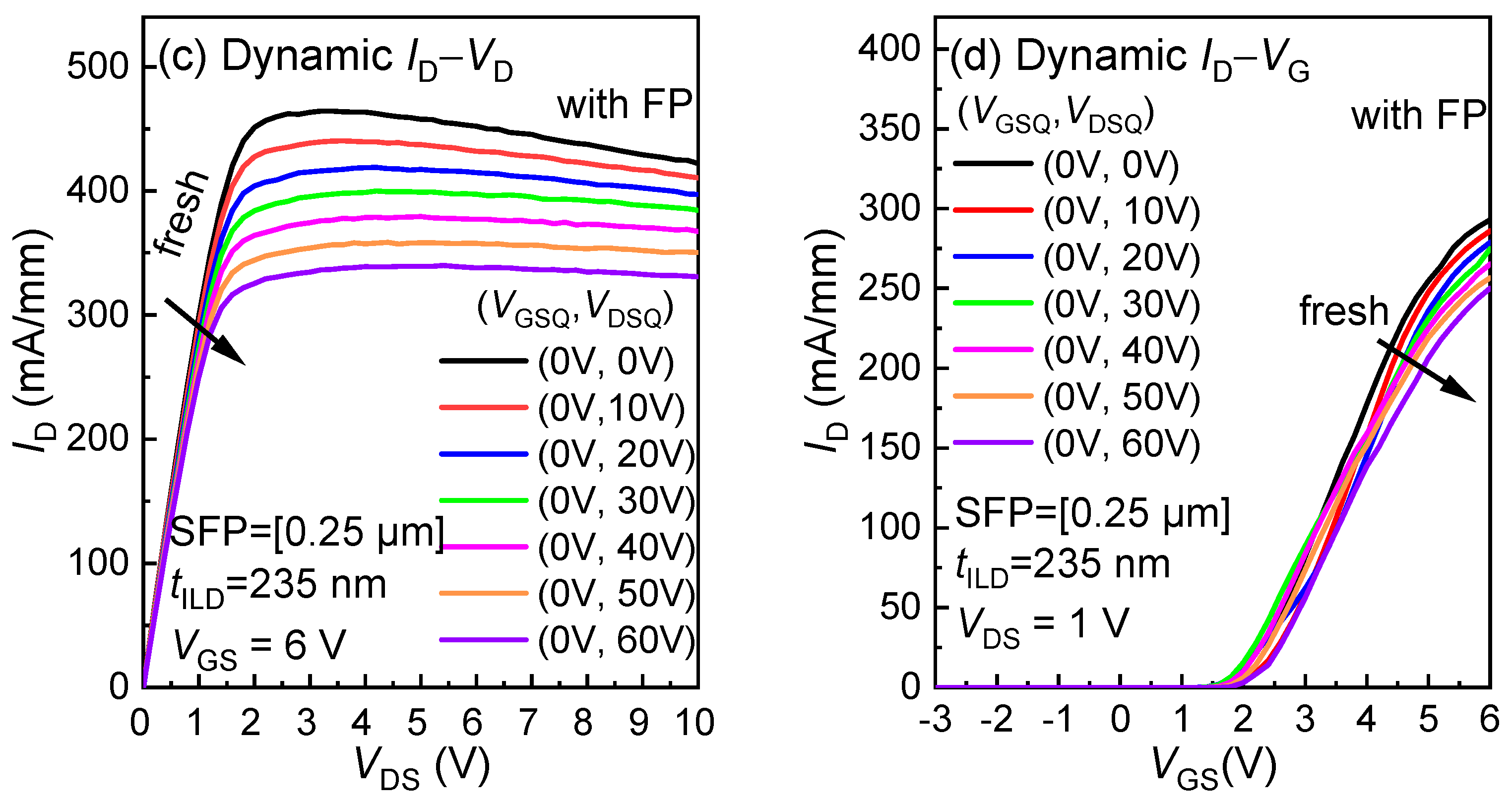
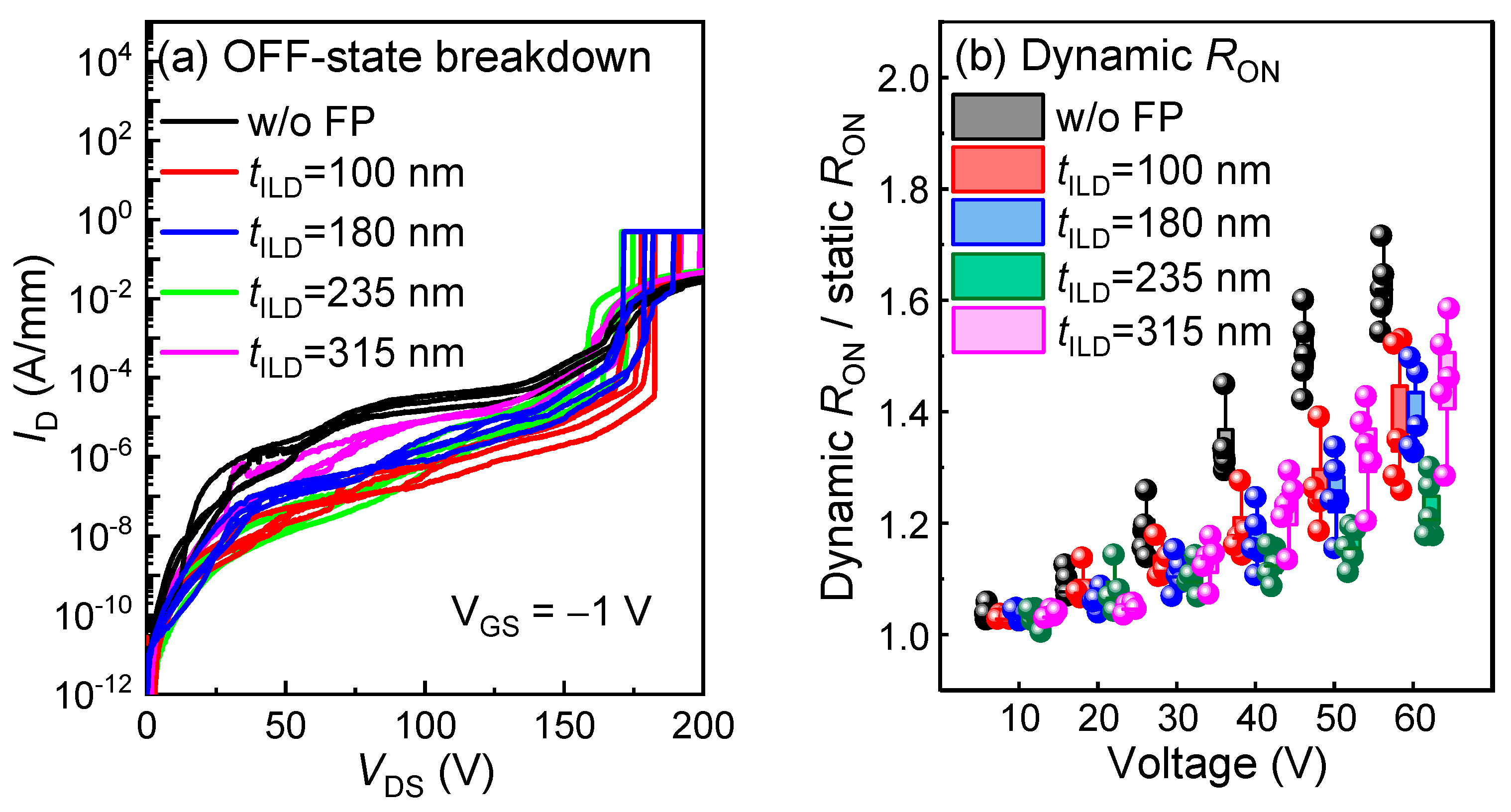
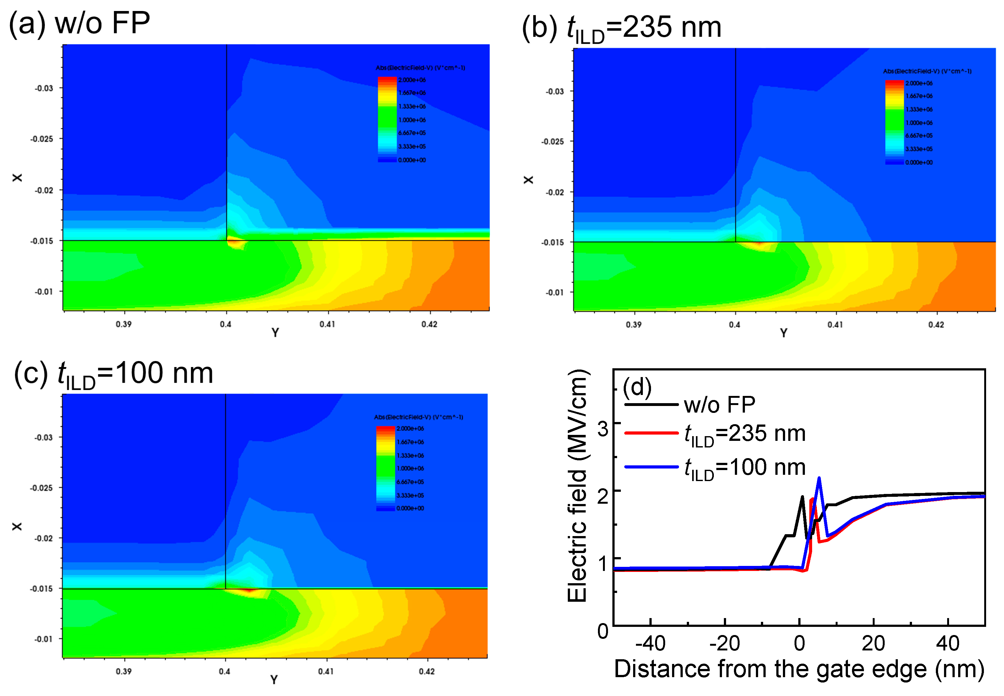
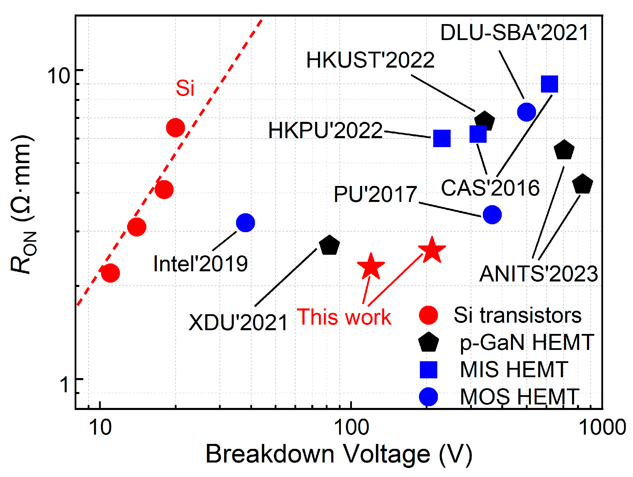
The p-GaN/AlGaN/GaN structure was epitaxially grown using metalorganic chemical vapor deposition (MOCVD) on 6-inch Si substrates, as shown in Figure 1. The epitaxy stack consists of an 80 nm Mg-doped p-GaN layer with a doping concentration of 3.4 × 1019 cm−3, a 15 nm Al0.25Ga0.75N barrier layer, a 400 nm GaN channel layer, a ~5 μm GaN buffer layer, and a 200 nm AlN nucleation layer, from top to bottom, which is depicted in Figure 2. The electron mobility extracted using Hall measurement at room temperature was 1452 cm2/Vs.
As shown in Figure 2, the CMOS-compatible process in our pilot line starts with the deposition of a 30 nm TiN layer on the p-GaN surface, followed by device isolation through multiple nitrogen ion implantation processes. Then, high-selectivity Cl2/BCl3/SF6-mixed gas plasma etching of the p-GaN was carried out. A 5 nm Al2O3 passivation layer was deposited using atomic layer deposition (ALD), and the SiO2 layer was deposited using plasma-enhanced chemical vapor deposition (PECVD). Ohmic contact window opening was performed through reactive ion etching (RIE), followed by Ohmic metal stack Ti/Al/Ti/TiN (5/100/20/60 nm) deposition using physical vapor deposition (PVD) and patterning via chlorine-based inductively coupled plasma etching (ICP). In Figure 3, the scanning electron microscope (SEM) image provides a cross-sectional view of the fabricated low-voltage p-GaN gate HEMTs.

3. Results

The output characteristics of the low-voltage HEMTs with an LGD of 1.5 µm and the transfer characteristics of the HEMTs with an LGD from 1 to 3 µm on the 6-inch wafer are presented in Figure 4a,b, where threshold voltage, VTH, and the ON-resistance, RON, reach 1.6 V and 2.8 Ω·mm, respectively. The current droop in the saturation region of the ID-VD curves possibly stems from the self-heating effect. In Figure 5, the electrical mapping and statistical distribution of the VTH and RON values of the 245 HEMTs across the 6-inch whole wafer are demonstrated. The VTH is concentrated in a range of 1.6 to 1.9 V, and the RON mainly falls between 2.6 and 3.2 Ω·mm, presenting excellent uniformity across the wafer.
Figure 6a depicts depth profiles of the Mg, H, and Al concentrations of the gate–stack regions obtained via secondary ion mass spectroscopy (SIMS). Capacitance–voltage (C-V) curves under various frequencies from 100 k to 1 MHz are shown in Figure 6b. The rising of the gate capacitance corresponds to the formation of the 2DEG channel, aligning with the ID-VG curves observed in Figure 4b. Furthermore, Figure 7a demonstrates the forward bias gate breakdown characteristics of the p-GaN gate HEMTs with an LG from 0.5 µm to 0.8 µm, showing that the forward gate breakdown voltage, VG-BD, exceeds 12 V, attributable to the optimized TiN retraction process, as shown in Figure 2 [22]. To further assess the gate stability, forward and reverse gate bias stress was applied to the HEMTs with an LGD of 1.5 µm. The VTH variation was monitored by a typical spot-ID sensing method, with the relaxation time between stressing and sensing limited to 1 ms [23]. As shown in Figure 7b, the p-GaN gate HEMTs exhibit a slight positive VTH shift under a gate bias stress of ≤5 V and a negative VTH shift under 6 V, probably stemming from a hole injection [24].
Figure 8a,b illustrate the OFF-state breakdown performance of the low-voltage p-GaN gate HEMTs. It can be observed that tuning the LG and the field plate can effectively reduce the OFF-state leakage of the p-GaN gate HEMTs. As shown in Figure 8c,d, both the OFF-state VBD and RON are linearly dependent on the LGD. In our design, the HEMTs with a simple device structure and an LGD of 1 µm exhibit an OFF-state VBD of up to 100 V and an RON value of 2.5 Ω·mm, which clears the way for designing and manufacturing ≤30 V p-GaN gate HEMTs in the future.
To evaluate the dynamic performance of the low-voltage devices with advanced Al2O3/SiO2 passivation and the impact of the ILD thickness, tILD, the dynamic characteristics of the HEMTs with an LGD of 1.5 µm were assessed by an AMCAD high-speed pulsed I-V system [25]. Figure 9a,b, respectively, show the pulse waveforms of the output and transfer characteristics measured by the pulsed I-V system. The pulse period was 3 ms, with a VDS pulse width of 17 µs, a VGS pulse width of 12 µs, and a sampling delay time of 9 µs, resulting in a duty cycle of 0.4% to suppress the self-heating effects [26]. A dead time of 2.5 µs was introduced between the edges of the drain and gate pulses to mimic soft-switching conditions. A sampling delay time of 9 µs was employed to filter out the transient instabilities of the waveforms that occurred immediately after the switching event. Within one cycle, OFF-state high-voltage stress with quiescent stressing voltages, VDSQ, of 0 to 60 V and a quiescent gate bias of 0 V was first applied to the devices. Then, the devices were immediately subjected to ON-state measurement.
Figure 10 illustrates the dynamic characteristics of the devices with and without field plates under quiescent stress conditions. The dynamic RON of the HEMTs without field a plate degraded by more than 60%, as shown in Figure 10a, while the value for HEMTs with a 0.25 µm source field plate (SFP) was only 16%, as shown in Figure 10c. It can be seen from Figure 10b,d that the VTH shift of the HEMTs with an SFP is significantly suppressed from 1.1 to 0.5 V. This is because the SFP can effectively smoothen the electric field distribution and weaken the high electric field peak at the drain-side gate edge, thus improving the dynamic performance of the low-voltage p-GaN gate HEMTs [21].
Next, to further optimize the dynamic performance and evaluate the impact of the ILD thickness, tILD, of the SiO2 passivation layer on the low-voltage p-GaN gate HEMTs with source field plates, four ILD thickness, tILD, values of 100, 180, 235, and 315 nm were prepared for the HEMTs with an LGD = 1.5 µm and source field plates of [X] = 0.25 µm. As shown in Figure 11a, the OFF-state breakdown voltages of the low-voltage devices exhibit a negligible dependence on the tILD. However, the devices with tILD = 315 nm show a higher OFF-state leakage current, indicating the electric field modulation effect of the source field plate is weakened by the thicker ILD layer.
Furthermore, the impact of the tILD on the dynamic characteristics was evaluated. It can be directly observed in Figure 11b that the dynamic RON does not show a monotonic relationship with the tILD. Specifically, when the tILD ≤ 235 nm, the dynamic RON decreases as tILD increases. However, when the tILD > 235 nm, the dynamic characteristics deteriorate with an increasing tILD. The dynamic RON degradation of the HEMTs with a low tILD probably stems from the interaction between the source field plate and the p-GaN gate edge [27]. For a high tILD, the dynamic RON deterioration can probably be attributed to the reduced electric field modulation effect of the source field plate caused by the large distance. To uncover the underlying mechanism, a Sentaurus technology computer-aided design (TCAD) simulation was conducted. As shown in Figure 12, the source field plate structure can effectively weaken the high electric field peak at the drain-side p-GaN edge. Impressively, the results reveal that the low tILD reduces the electric fields at the edges of the p-GaN but strengthens the peak electric field. Overall, for the low-voltage p-GaN gate HEMTs with LGD = 1.5 µm and SFP = [0.25 µm], a tILD of 235 nm delivers the best dynamic characteristics in our work.
Figure 13 benchmarks the VBD versus RON of this work against other results [28,29,30,31,32]. The low-voltage p-GaN gate HEMTs in this work not only maintained high VBD and high reliability but also achieved a low RON by optimizing the field plate structure.

4. Conclusions

AI-driven high-reliability and high-performance low-voltage p-GaN gate HEMTs have been successfully fabricated on 6-inch Si using a CMOS-compatible process in our pilot line. This research shows that by engineering the source field plate structure and optimizing the interlayer dielectric thickness, the dynamic RON degradation of the devices was suppressed from 60% to 20%, and the VTH shift of the HEMTs was significantly reduced from 1.1 to 0.5 V. An interlayer thickness of 235 nm provided the best dynamic performance for the 60 V p-GaN gate HEMTs with an LGD of 1.5 µm and SFP = 0.25 µm, which not only maintained high reliability and a high VBD over 180 V but also achieved a lower RON of 2.8 Ω·mm. These findings provide directional guidance for the future fabrication of high-performance devices, crucial in enabling more energy-efficient, high-performance, and miniaturized secondary power solutions, ultimately supporting the sustainable growth of AI infrastructure.

Author Contributions

Device design, L.Z., X.L., J.W. and Z.H.; fabrication, J.J. and X.L.; characterization, L.Z., Z.H., L.Y., L.C., H.X., X.J., T.Z. and S.Y.; writing original draft preparation, L.Z., X.L., Y.C., J.Z. and Y.H. All authors have read and agreed to the published version of the manuscript.

Funding

This research was funded in part by the National Key Research and Development Program of China under Grant 2021YFB3600900, in part by the Guangdong Basic and Applied Basic Research Foundation under Grant 2023A1515110801, in part by the Zhuhai Industry University Research Cooperation Project under Grant 2320004002835, and in part by the Natural Science Basic Research Program of Shaanxi under Grant 2024JC-YBQN-0621. (Corresponding author: Xiangdong Li; Jincheng Zhang.)

Data Availability Statement

The data that support the findings of this study are available from the corresponding authors upon reasonable request.

Acknowledgments

The authors thank all members of the GaN Power Electronics Research Group, especially Xiangdong Li, Shuzhen You, and Jian Ji from the Guangzhou Institute of Technology, Xidian University.

Conflicts of Interest

The authors declare no conflicts of interest.

References

  1. Musumeci, S.; Mandrile, F.; Barba, V.; Palma, M. Low-voltage GaN FETs in motor control application; issues and advantages: A review. Energies 2021, 14, 6378. [Google Scholar] [CrossRef]
  2. Han, T.; Peng, X.; Zhang, W.; Wang, T.; Yang, L.; Zhao, P. Effects of physical parameters of graded AlGaN buffer on DC characteristic and short-channel effects in AlInN/GaN high-electron mobility transistors. Microelectron. J. 2023, 139, 105881. [Google Scholar] [CrossRef]
  3. Xin, Y.; Chen, W.; Sun, R.; Deng, X.; Li, Z.; Zhang, B. Barrier Lowering-Induced Capacitance Increase of Short-Channel Power p-GaN HEMTs at High Temperature. IEEE Trans. Electron. Devices 2022, 69, 1176–1180. [Google Scholar] [CrossRef]
  4. Then, H.W.; Koirala, P.; Varghese, L.; Zubair, A.; Bader, S.; Beumer, M.; Vora, H.; Golani, P.; Peck, J.; Hoff, T.; et al. 30nm Channel-Length Enhancement-Mode GaN MOSHEMT Transistors on a 300mm GaN-on-TRSOI Engineered Substrate. In Proceedings of the 2024 IEEE International Electron Devices Meeting (IEDM), San Francisco, CA, USA, 7–11 December 2024; pp. 1–4. [Google Scholar]
  5. Posthuma, N.; You, S.; Liang, H.; Ronchi, N.; Kang, X.; Wellekens, D.; Saripalli, Y.; Decoutere, S. Impact of Mg out-diffusion and activation on the p-GaN gate HEMT device performance. In Proceedings of the 2016 28th International Symposium on Power Semiconductor Devices and ICs (ISPSD), Prague, Czech Republic, 12–16 June 2016; pp. 95–98. [Google Scholar]
  6. Kozak, J.P.; Zhang, R.; Porter, M.; Song, Q.; Liu, J.; Wang, B.; Wang, R.; Saito, W.; Zhang, Y. Stability, Reliability, and Robustness of GaN Power Devices: A Review. IEEE Trans. Power Electron. 2023, 38, 8442–8471. [Google Scholar] [CrossRef]
  7. Tang, S.; Bakeroot, B.; Huang, Z.; Chen, S.; Lin, W.; Lo, T.; Borga, M.; Wellekens, D.; Posthuma, N.; Decoutere, S.; et al. Using gate leakage conduction to understand positive gate bias induced threshold voltage shift in p-GaN gate HEMTs. IEEE Trans. Electron Devices 2023, 70, 449–453. [Google Scholar] [CrossRef]
  8. Wei, Y.-T.; Chou, H.-C.; Wu, Y.-H.; Yang, F.; Lee, C.-H. Demonstration of Schottky barrier diode integrated in 200 V power p-GaN HEMTs technology with robust stability. IEEE J. Electron Devices Soc. 2016, 4, 37–41. [Google Scholar]
  9. Huang, Y.-C.; Chen, G.-R.; Chen, K.-M. 200 V enhancement-mode p-GaN HEMTs fabricated on 200 mm GaN-on-SOI with trench isolation for monolithic integration. IEEE J. Electron Devices Soc. 2017, 5, 10–16. [Google Scholar]
  10. Wong, K.; Hao, R.; Chou, A.; Zou, Y.; Shen, J.; Li, S.; Yang, C.; Zhang, A.; Hu, T.; Chen, F. Comprehensive GaN-on-Si power device platform: Epitaxy, device, reliability and application. Semicond. Sci. Technol. 2021, 36, 064001. [Google Scholar] [CrossRef]
  11. Ashourloo, M.; Zaman, M.S.; Nasr, M.; Trescases, O. Opportunities for leveraging low-voltage GaN devices in modular multi-level converters for electric-vehicle charging applications. In Proceedings of the 2018 International Power Electronics Conference, Niigata, Japan, 20–24 May 2018; pp. 2380–2385. [Google Scholar]
  12. Shen, J.; Jing, L.; Qiu, J. High-frequency full-bridge 48V DC-5V DC LLC resonant converter with AlGaN/GaN HEMTs. In Proceedings of the 2023 5th International Conference on Electrical Engineering and Control Technologies (CEECT), Chengdu, China, 15–17 December 2023; pp. 338–342. [Google Scholar]
  13. Wu, S.; Ran, Z.; Tong, Z.; Liu, T.; Lu, Y. A monolithic integrated E-mode GaN 48V-to-1V DC-DC buck converter with PWM control. In Proceedings of the 2023 IEEE International Conference on Integrated Circuits, Technologies and Applications (ICTA), Hefei, China, 27–29 October 2023; pp. 130–131. [Google Scholar]
  14. EPC2100—Enhancement-Mode GaN Power Transistor Half-Bridge. Available online: https://epc-co.com/epc/products/gan-fets-and-ics/epc2100 (accessed on 23 April 2021).
  15. Wang, T.; Jiang, L.; Zhang, M.; Jiang, Y. A novel physics-based approach to analyze and model E-mode p-GaN power HEMTs. IEEE Trans. Power Electron. 2019, 34, 1524–1534. [Google Scholar]
  16. Zhou, Y.; Zhu, J.; Mi, M.; Zhang, M.; Wang, P.; Han, Y.; Wu, S.; Liu, J.; Zhu, Q.; Chen, Y. Analysis of low voltage RF power capability on AlGaN/GaN and InAlN/GaN HEMTs for terminal applications. IEEE J. Electron Devices Soc. 2021, 9, 756–762. [Google Scholar] [CrossRef]
  17. Zanoni, E.; Santi, C.D.; Gao, Z.; Buffolo, M.; Fornasier, M.; Saro, M.; Pieri, F.D. Microwave and millimeter-wave GaN HEMTs: Impact of epitaxial structure on short-channel effects, electron trapping, and reliability. IEEE Trans. Electron Devices 2024, 71, 1396–1407. [Google Scholar] [CrossRef]
  18. Hu, Y.; Hernández-Gutiérre, C.; Solís-Cisneros, H.; Santana, G.; Kudriatsev, Y.; Camas-Anzueto, J.; López-López, M. Blue luminescence origin and Mg acceptor saturation in highly doped zinc-blende GaN with Mg. J. Alloys Compd. 2022, 897, 163133. [Google Scholar] [CrossRef]
  19. Zhang, L.; Zheng, Z.; Yang, S.; Song, W.; He, J.; Chen, K.J. p-GaN gate HEMT with surface reinforcement for enhanced gate reliability. IEEE Electron Device Lett. 2020, 42, 22–25. [Google Scholar] [CrossRef]
  20. Li, X.; Wang, J.; Zhang, J.; Han, Z.; You, S.; Chen, L.; Wang, L.; Li, Z.; Yang, W.; Chang, J. 1700 V high-performance GaN HEMTs on 6-inch sapphire with 1.5 μm thin buffer. IEEE Electron Device Lett. 2024, 45, 84–87. [Google Scholar] [CrossRef]
  21. Gupta, S.D.; Joshi, V.; Chaudhuri, R.R.; Shrivastava, M. Part I: Physical insights into dynamic R_ON behavior and a unique time-dependent critical stress voltage in AlGaN/GaN HEMTs. IEEE Trans. Electron Devices 2021, 68, 5720–5727. [Google Scholar] [CrossRef]
  22. Han, Z.; Li, X.; Ji, J.; Chen, L.; Wang, L.; Cheng, Z.; Yang, W.; You, S.; Li, Z.; Hao, Y. p-GaN gate HEMTs on 6-inch sapphire by CMOS-compatible process: A promising game changer for power electronics. IEEE Electron Device Lett. 2024, 45, 1257–1260. [Google Scholar] [CrossRef]
  23. Gao, R.; Shi, Y.; He, Z.; Chen, Y.; En, Y.; Huang, Y.; Ji, Z.; Zhang, J.; Zhang, W.; Zheng, X.; et al. A fast extraction method of energy distribution of border traps in AlGaN/GaN MIS-HEMT. IEEE J. Electron Devices Soc. 2020, 8, 905–910. [Google Scholar] [CrossRef]
  24. Tang, X.; Li, B.; Moghadam, H.A.; Tanner, P.; Han, J.; Dimitrijev, S. Mechanism of threshold voltage shift in p-GaN gate AlGaN/GaN transistors. IEEE Electron Device Lett. 2018, 39, 1145–1148. [Google Scholar] [CrossRef]
  25. Wang, Y.; Hua, M.; Tang, G.; Lei, J.; Zheng, Z.; Wei, J.; Chen, K. Dynamic OFF-State Current (Dynamic IOFF) in p-GaN Gate HEMTs With an Ohmic Gate Contact. IEEE Electron Device Lett. 2018, 39, 1366–1369. [Google Scholar] [CrossRef]
  26. Wang, Y.; Lyu, G.; Wei, J.; Zheng, Z.; He, J.; Lei, J.; Chen, K.J. Characterization of static and dynamic behavior of 1200 V normally off GaN/SiC cascode devices. IEEE Trans. Ind. Electron. 2019, 67, 10284–10294. [Google Scholar] [CrossRef]
  27. Song, J.; Wang, M.; Wei, J.; Fan, Z.; Zhang, J.; Yang, H.; Wang, P.; Xie, B.; Li, C.; Yuan, L. Effect of source electrostatic interaction on the off-state leakage current of p-GaN gate HEMTs. IEEE Electron Device Lett. 2024, 45, 1728–1731. [Google Scholar] [CrossRef]
  28. He, J.; Wang, Q.; Zhou, G.; Li, W.; Jiang, Y.; Qiao, Z.; Tang, C.; Li, G.; Yu, H. Normally-OFF AlGaN/GaN MIS-HEMTs With Low RON and Vth Hysteresis by Functioning In-situ SiNx in Regrowth Process. IEEE Electron Device Lett. 2022, 43, 529–532. [Google Scholar] [CrossRef]
  29. Liao, H.; Zheng, Z.; Chen, T.; Zhang, L.; Cheng, Y.; Feng, S.; Ng, Y.; Chen, L.; Yuan, L.; Chen, K. Normally-OFF p-GaN Gate Double-Channel HEMT With Suppressed Hot-Electron-Induced Dynamic ON-Resistance Degradation. IEEE Electron Device Lett. 2022, 43, 1424–1427. [Google Scholar] [CrossRef]
  30. Zhou, G.; Zeng, F.; Jiang, Y.; Wang, Q.; Jiang, L.; Xia, G.; Yu, H. Determination of the Gate Breakdown Mechanisms in p-GaN Gate HEMTs by Multiple-Gate-Sweep Measurements. IEEE Trans. Electron Devices 2021, 68, 1518–1523. [Google Scholar] [CrossRef]
  31. Revathy, A.; Vijaya Kumar, J.; Murugapandiyan, P.; Wasim, M.; Nirmala Devi, K.; Ramkumar, N. Design and analysis of normally-off GaN-HEMT using β-Ga2O3 buffer for low-loss power converter applications. Micro Nanostructures 2023, 182, 207643. [Google Scholar] [CrossRef]
  32. Then, H.W.; Dasgupta, S.; Radosavljevic, M.; Agababov, P.; Ban, I.; Bristol, R.; Chandhok, M.; Chouksey, S.; Holybee, B.; Huang, C.Y.; et al. 3D heterogeneous integration of high performance high-K metal gate GaN NMOS and Si PMOS transistors on 300 mm high-resistivity Si substrate for energy-efficient and compact power delivery, RF (5G and beyond) and SoC applications. In Proceedings of the 2019 IEEE International Electron Devices Meeting (IEDM), San Francisco, CA, USA, 7–11 December 2019; pp. 17.3.1–17.3.4. [Google Scholar]
Figure 1. Photograph of the 6-inch wafer manufactured using the CMOS-compatible process.
Micromachines 16 00556 g001
Figure 2. Cross-sectional schematic and process flow of the p-GaN gate HEMTs on the 6-inch Si substrate. [X] denotes the field plate structure.
Micromachines 16 00556 g002
Figure 3. SEM image of the low-voltage p-GaN gate HEMTs.
Micromachines 16 00556 g003
Figure 4. (a) Output characteristics of the p-GaN gate HEMTs with LGD of 1.5 µm; (b) transfer characteristics of the p-GaN gate HEMTs with LGD of 1 µm to 3 µm.
Micromachines 16 00556 g004
Figure 5. (a) Electrical mapping and (c) statistical distribution of VTH; (b) electrical mapping and (d) statistical distribution of RON of 245 devices with LGD = 1.5 µm across the 6-inch wafer.
Micromachines 16 00556 g005
Figure 6. (a) SIMS profiles of the Mg, H, and Al concentrations vertically along the gate–stack of p-GaN/AlGaN/GaN; (b) frequency-dependent C-V characteristic curves.
Micromachines 16 00556 g006
Figure 7. (a) Forward bias gate breakdown characteristics; (b) ΔVTH versus stress time under various reverse and forward gate bias stresses of the low-voltage p-GaN gate HEMTs.
Micromachines 16 00556 g007
Figure 8. OFF-state breakdown characteristics with (a) LG of 0.5/0.6/0.7/0.8 µm and (b) LGD of 1/1.5/2/2.5/3 µm; the statistical distribution of (c) VBD and (d) RON versus LGD for the low-voltage p-GaN gate HEMTs on 6-inch Si.
Micromachines 16 00556 g008
Figure 9. Schematic waveforms of VGS and VDS in the pulsed I-V tests of (a) output and (b) transfer characteristics.
Micromachines 16 00556 g009
Figure 10. Pulsed (a) ID-VD and (b) ID-VG curves of p-GaN gate HEMTs without field plates; pulsed (c) ID-VD and (d) ID-VG curves of 1-FP p-GaN gate HEMTs with SFP = 0.25 µm and LGD of 1.5 µm under various quiescent stress conditions.
Micromachines 16 00556 g010aMicromachines 16 00556 g010b
Figure 11. (a) OFF-state breakdown curves and (b) dynamic RON under various OFF-state stress voltages for five HEMTs structures with LGD of 1.5 µm.
Micromachines 16 00556 g011
Figure 12. OFF-state electric field simulation under VDS of 60 V for HEMTs with LGD of 1.5 µm for (a) w/o FP, 1-FP of (b) tILD = 235 nm, and (c) tILD = 100 nm; (d) the simulated electric field strength.
Micromachines 16 00556 g012
Figure 13. Benchmark plot of VBD versus RON.
Micromachines 16 00556 g013
Disclaimer/Publisher’s Note: The statements, opinions and data contained in all publications are solely those of the individual author(s) and contributor(s) and not of MDPI and/or the editor(s). MDPI and/or the editor(s) disclaim responsibility for any injury to people or property resulting from any ideas, methods, instructions or products referred to in the content.

