
Research Progress on Micromachining Technologies Used to Fabricate Terahertz Micro-Metallic Rectangular Cavity Structures

Abstract
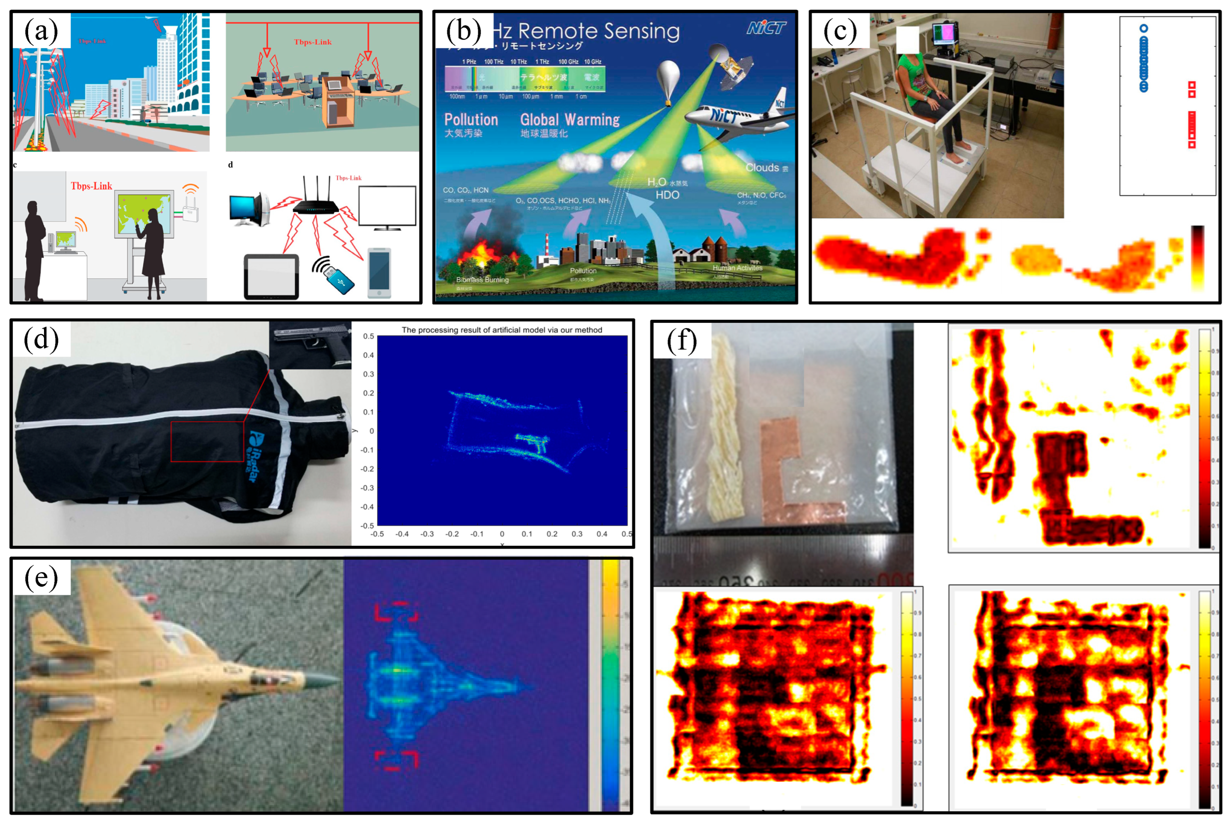
1. Introduction
2. Description of Typical Terahertz Metallic Rectangular Cavity Structures
3. Manufacturing Technologies Used to Fabricate Terahertz Metallic Rectangular Cavity Structures
3.1. Deep Reactive Ion Etching
3.2. UV-LIGA Technology
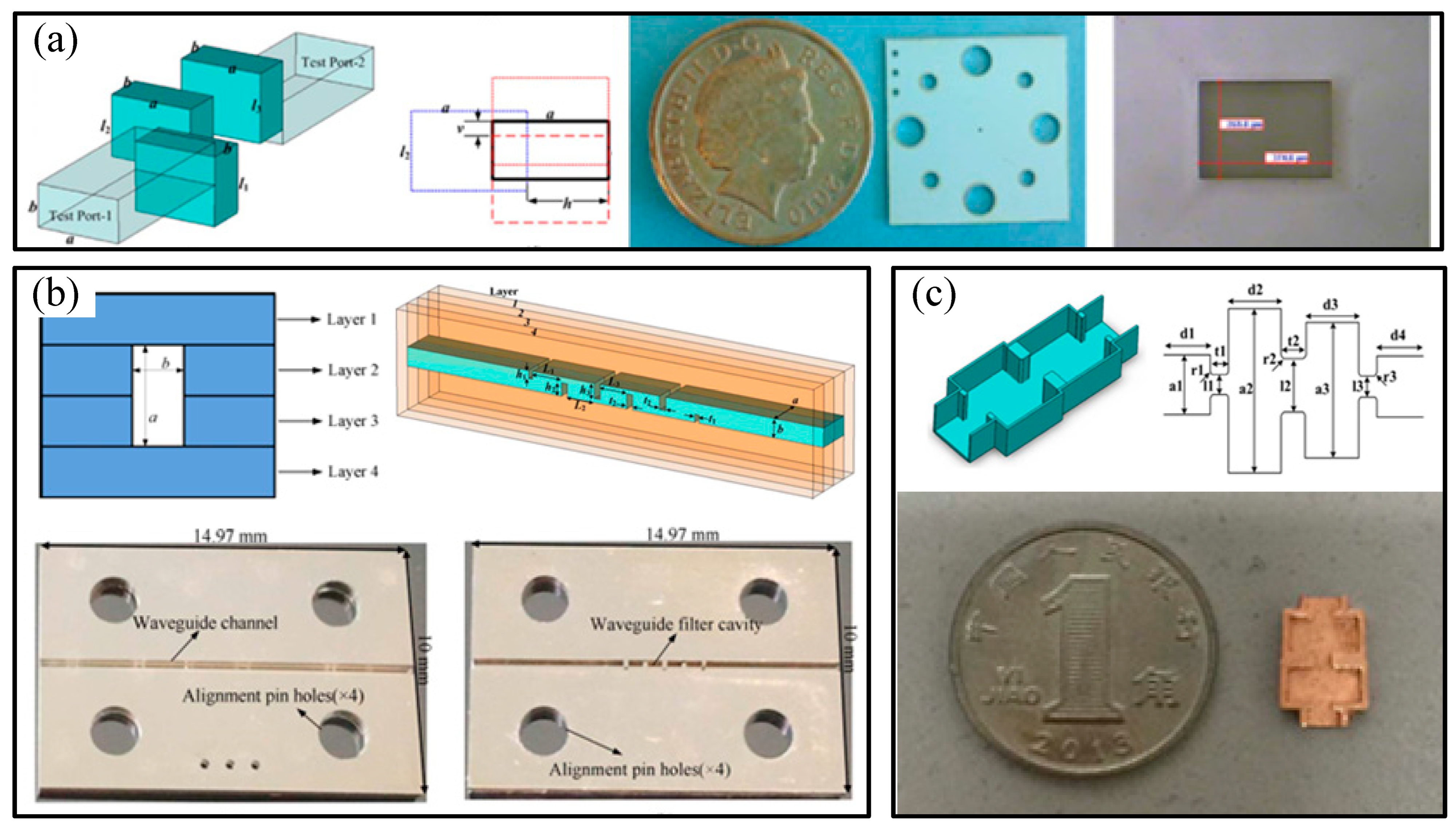
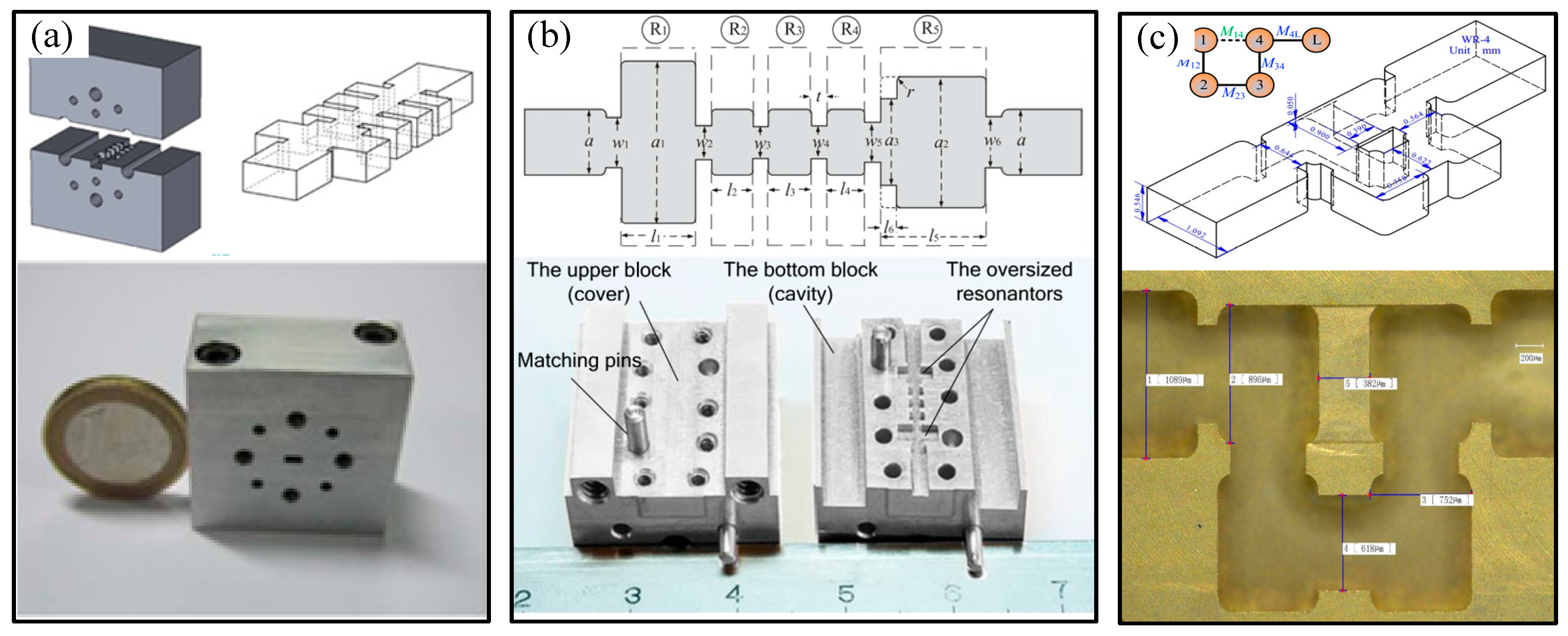
3.3. Micro-Milling Technology
3.4. LTCC Technology
3.5. Three-Dimensional Printing Technology
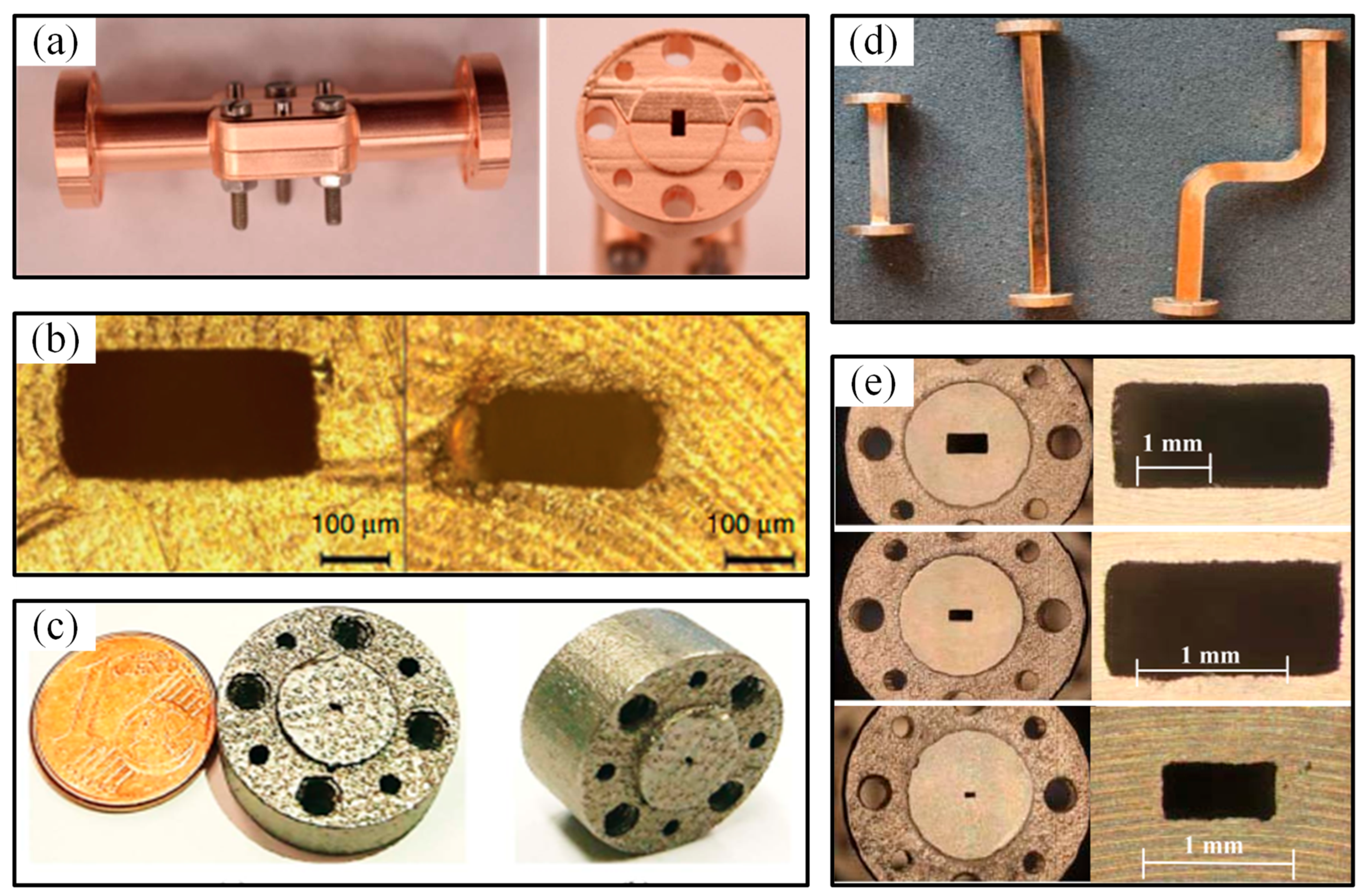
3.6. Electrochemical Micromachining Technology
4. Conclusions
Author Contributions
Funding
Conflicts of Interest
References
- Zhang, J.; Li, S.; Le, W. Advances of terahertz technology in neuroscience: Current status and a future perspective. iScience 2021, 24, 103548. [Google Scholar] [CrossRef] [PubMed]
- Hong, G.; Li, S. Development and future prospects of arthritis imaging. Chin. J. Radiol. 2024, 58, 1286–1291. [Google Scholar]
- Jin, Z.; Lou, J.; Shu, F.; Hong, Z.; Qiu, C. Advances in Nanoengineered Terahertz Technology: Generation, Modulation, and Bio-Applications. Research 2025, 8, 0562. [Google Scholar] [CrossRef]
- Li, J.; Deng, X.; Li, Y.; Hu, J.; Miao, W.; Lin, C.; Jiang, J.; Shi, S. Terahertz Science and Technology in Astronomy, Telecommunications, and Biophysics. Research 2025, 8, 0586. [Google Scholar] [CrossRef]
- Wang, H. Light People: Professor Xi-Cheng Zhang. Light Sci. Appl. 2022, 11, 272. [Google Scholar] [CrossRef] [PubMed]
- Masanori, H. Development and future prospects of terahertz technology. Jpn. J. Appl. Phys. 2015, 54, 120101. [Google Scholar] [CrossRef]
- Mohammadzadeh, S.; Hussung, R.; Keil, A.; Leuchs, S.; Krebs, C.; Nüβler, D.; Seewig, J.; Von Freymann, G.; Friederich, F. Compact hand-guided 3D scanning terahertz sensor platforms with 3D-printed aspherical telecentric f-θ lens. Int. J. Microw. Wirel. Technol. 2023, 15, 1027–1037. [Google Scholar] [CrossRef]
- Chow, B.J.; Liu, C.; Yu, M.; Xin Yu Lee, I.; Mehta, J.S.; Wu, Q.Y.S.; Wong Kay Ting, R.; Lin, K.; Liu, Y.C. The Application of Terahertz Technology in Corneas and Corneal Diseases: A Systematic Review. Bioengineering 2025, 12, 45. [Google Scholar] [CrossRef]
- Li, A.; Yang, Y.; Wu, S.; Vogt Wu, T.; Zhang, Y.; Wu, W.; Zhang, H. Study on non-destructive detection technology of water content and defects in construction materials based on transmission terahertz system. J. Build. Eng. 2025, 104, 112452. [Google Scholar] [CrossRef]
- Kikuchi, R.; Nakagawa, S.; Enomoto, Y.; Kuzumi, Y.; Yamada, S.; Maeshima, K.; Yamauchi, Y.; Minami, H.; Kashiwagi, T. Evaluation of the device characteristics of Bi2Sr2CaCu2O8+δ terahertz-wave emitters using wet-etching techniques. J. Appl. Phys. 2025, 137, 043908. [Google Scholar] [CrossRef]
- You, B.; Hsieh, C.C.; Lin, Y.S.; Lu, P.J.; Tsai, H.Y.; Yu, L.C.; Chang, S.Y.; Wu, Y.C.; Liang, Z.Q. Refractive-index sensing based on terahertz cavity-modal confinement of Bragg metal grating structure. Phys. Scr. 2025, 100, 035551. [Google Scholar] [CrossRef]
- Ouchi, A.; Tripathi, S.R. Terahertz Circular Dichroism Spectroscopy of 3D Chiral Metallic Microstructures Fabricated Using High Precision CNC Machining. IEEE J. Microw. 2025, 5, 108–115. [Google Scholar] [CrossRef]
- Sarieddeen, H.; Saeed, N.; Al-Naffouri, T.Y.; Alouini, M.S. Next generation terahertz communications: A rendezvous of sensing, imaging, and localization. IEEE Commun. Mag. 2020, 58, 69–75. [Google Scholar] [CrossRef]
- Huang, Y.; Shen, Y.; Wang, J. From Terahertz Imaging to Terahertz Wireless Communications. Engineering 2023, 22, 106–124. [Google Scholar] [CrossRef]
- Akkaş, M.A. Terahertz wireless data communication. Wirel. Netw. 2019, 25, 145–155. [Google Scholar] [CrossRef]
- Liang, M.; Ren, Z.; Zhang, C. Progress of Terahertz Space Exploration Technology. Laser. Optoelectron. Prog. 2019, 56, 18. [Google Scholar]
- Hosako, I.; Sekine, N.; Patrashin, M.; Saito, S.; Fukunaga, K.; Kasai, Y.; Baron, P.; Seta, T.; Mendrok, J.; Ochiai, S.; et al. At the dawn of a new era in terahertz technology. Proc. IEEE 2007, 95, 1611–1623. [Google Scholar] [CrossRef]
- Satpathy, S.; Khalaf, O.I.; Shukla, D.K.; Algburi, S.; Hamam, H. Consumer electronics based smart technologies for enhanced terahertz healthcare having an integration of split learning with medical imaging. Sci. Rep. 2024, 14, 1–12. [Google Scholar] [CrossRef]
- Pickwell-MacPherson, E.; Wallace, V.P. Terahertz pulsed imaging-A potential medical imaging modality. Photodiagnosis Photodyn. Ther. 2009, 6, 128–134. [Google Scholar] [CrossRef]
- Hernandez-Cardoso, G.G.; Rojas-Landeros, S.C.; Alfaro-Gomez, M.; Hernandez-Serrano, A.I.; Salas-Gutierrez, I.; Lemus-Bedolla, E.; Castillo-Guzman, A.R.; Lopez-Lemus, H.L.; Castro-Camus, E. Terahertz imaging for early screening of diabetic foot syndrome: A proof of concept. Sci. Rep. 2017, 7, 10412. [Google Scholar] [CrossRef]
- Zhan, M.; Wu, J.; Li, Y.; Xu, G.; Zhu, Y. An Adaptive Nonlinear Phase Error Estimation and Compensation Method for Terahertz Radar Imaging System. IEEE J. Miniaturization Air Sp. Syst. 2024, 5, 108–116. [Google Scholar] [CrossRef]
- Cooper, K.B.; Dengler, R.J.; Llombart, N.; Bryllert, T.; Chattopadhyay, G.; Mehdi, I.; Siegel, P.H. An approach for sub-second imaging of concealed objects using terahertz (THz) radar. J. Infrared Millim. Terahertz Waves 2009, 30, 1297–1307. [Google Scholar] [CrossRef]
- Gui, S.; Li, J.; Pi, Y. Security Imaging for Multi-Target Screening Based on Adaptive Scene Segmentation with Terahertz Radar. IEEE Sens. J. 2019, 19, 2675–2684. [Google Scholar] [CrossRef]
- Liu, T.; Pi, Y.; Yang, X. Wide-Angle CSAR Imaging Based on the Adaptive Subaperture Partition Method in the Terahertz Band. IEEE Trans. Terahertz Sci. Technol. 2018, 8, 165–173. [Google Scholar] [CrossRef]
- Guo, C.; Xu, W.; Cai, M.; Duan, S.; Fu, J.; Zhang, X. A Review: Application of Terahertz Nondestructive Testing Technology in Electrical Insulation Materials. IEEE Access 2022, 10, 121547–121560. [Google Scholar] [CrossRef]
- Han, S.T. Application of a Compact Sub-Terahertz Gyrotron for Nondestructive Inspections. IEEE Trans. Plasma Sci. 2020, 48, 3238–3245. [Google Scholar] [CrossRef]
- Wu, Y.Q.; Chen, M.Y.; Dai, Z.J. Review on the terahertz transmission devices and their applications: From metal waveguides to terahertz fibers. Opt. Laser Technol. 2025, 183, 112339. [Google Scholar] [CrossRef]
- Katyba, G.M.; Zaytsev, K.I.; Dolganova, I.N.; Chernomyrdin, N.V.; Ulitko, V.E.; Rossolenko, S.N.; Shikunova, I.A.; Kurlov, V.N. Sapphire waveguides and fibers for terahertz applications. Prog. Cryst. Growth Charact. Mater. 2021, 67, 100523. [Google Scholar] [CrossRef]
- Zhang, L.; Jiang, Y.; Lei, W.; Hu, P.; Guo, J.; Song, R.; Tang, X.; Ma, G.; Chen, H.; Wei, Y. A piecewise sine waveguide for terahertz traveling wave tube. Sci. Rep. 2022, 12, 10449. [Google Scholar] [CrossRef]
- Wang, C.; Wen, P.; Huang, X.; Chen, K.; Xu, K.-D. Terahertz dual-band bandpass filter based on spoof surface plasmon polaritons with wide upper stopband suppression. Opt. Express 2024, 32, 22748. [Google Scholar] [CrossRef]
- Yuan, J.; Ning, T.; Li, H.; Pei, L.; Li, J.; Zheng, J.; Wan, L. Terahertz filters based on subwavelength polymer waveguide. Results Phys. 2019, 13, 102198. [Google Scholar] [CrossRef]
- Liang, J.; Gao, W.; Lees, H.; Withayachumnankul, W. All-Silicon Terahertz Planar Horn Antenna. IEEE Antennas Wirel. Propag. Lett. 2021, 20, 2181–2185. [Google Scholar] [CrossRef]
- Lier, E. Review of soft and hard horn antennas, including metamaterial-based hybrid-mode horns. IEEE Antennas Propag. Mag. 2010, 52, 31–39. [Google Scholar] [CrossRef]
- Wu, G.B.; Chen, J.; Yang, C.; Chan, K.F.; Chen, M.K.; Tsai, D.P.; Chan, C.H. 3-D-Printed Terahertz Metalenses for Next-Generation Communication and Imaging Applications. Proc. IEEE 2024, 112, 1033–1050. [Google Scholar] [CrossRef]
- Li, Y.; Wang, Y.; Li, H.; Jiang, B.; Bai, F.; Feng, J. Terahertz Rectangular Waveguides by UV-LIGA with Megasonic Agitation. Micromachines 2022, 13, 1601. [Google Scholar] [CrossRef] [PubMed]
- Xu, J.; Ding, J.Q.; Zhao, Y.; Ge, J.X. W-Band Broadband Waveguide Filter Based on H-Plane Offset Coupling. J. Infrared Millim. Terahertz Waves 2019, 40, 412–418. [Google Scholar] [CrossRef]
- Gao, P.; Lu, Z.; Duan, J.; Zhu, J.; Wang, Z.; Gong, H.; Gong, Y. A Novel Folded Rectangular-Grating Slow Wave Structure for Dual-Beam Traveling Wave Tube. IEEE Trans. Electron Devices 2023, 70, 2730–2737. [Google Scholar] [CrossRef]
- Olivova, J.; Popela, M.; Richterova, M.; Blazek, V. Use of 3D Printing for Sierpinski Fractal Antenna Manufacturing. Electronics 2022, 11, 1539. [Google Scholar] [CrossRef]
- Zheng, Z.; Hu, J.; Liu, S.; Zhang, Y. WR-1.5 band waveguide bandpass dual-mode filter on silicon micromachining technique. In Proceedings of the 2015 IEEE International Conference on Communication Problem-Solving (ICCP), Guilin, China, 16–18 October 2015; pp. 112–114. [Google Scholar]
- Gerhard, M.; Beigang, R.; Rahm, M. Comparative Terahertz Study of Rectangular Metal Waveguides With and Without a Ridge. J. Infrared Millim. Terahertz Waves 2015, 36, 327–334. [Google Scholar] [CrossRef]
- Li, B.; Li, C.; Zhao, Y.; Han, C.; Zhang, Q. Deep reactive ion etching of Z-Cut alpha quartz for MEMS resonant devices fabrication. Micromachines 2020, 11, 724. [Google Scholar] [CrossRef]
- Chen, Z.; Zheng, Y.; Kang, X.; Lu, B.; Cui, B. WR-2.8 band micromachined rectangular waveguide filter. J. Infrared Millim. Terahertz Waves 2013, 34, 847–855. [Google Scholar] [CrossRef]
- Jung-Kubiak, C.; Reck, T.J.; Siles, J.V.; Lin, R.; Lee, C.; Gill, J.; Cooper, K.; Mehdi, I.; Chattopadhyay, G. A Multistep DRIE Process for Complex Terahertz Waveguide Components. IEEE Trans. Terahertz Sci. Technol. 2016, 6, 690–695. [Google Scholar] [CrossRef]
- Bagolini, A.; Ronchin, S.; Bellutti, P.; Chistè, M.; Verotti, M.; Belfiore, N.P. Fabrication of Novel MEMS Microgrippers by Deep Reactive Ion Etching With Metal Hard Mask. J. Microelectromechanical Syst. 2017, 26, 926–934. [Google Scholar] [CrossRef]
- Leong, K.M.K.H.; Hennig, K.; Zhang, C.; Elmadjian, R.N.; Zhou, Z.; Gorospe, B.S.; Chang-Chien, P.P.; Radisic, V.; Deal, W.R. WR1.5 silicon micromachined waveguide components and active circuit integration methodology. IEEE Trans. Microw. Theory Tech. 2012, 60, 998–1005. [Google Scholar] [CrossRef]
- Beuerle, B.; Campion, J.; Shah, U.; Oberhammer, J. A Very Low Loss 220-325 GHz Silicon Micromachined Waveguide Technology. IEEE Trans. Terahertz Sci. Technol. 2018, 8, 248–250. [Google Scholar] [CrossRef]
- Hu, J.; Xie, S.; Zhang, Y. Micromachined terahertz rectangular waveguide bandpass filter on silicon-substrate. IEEE Microw. Wirel. Compon. Lett. 2012, 22, 636–638. [Google Scholar] [CrossRef]
- Zhao, X.H.; Bao, J.F.; Shan, G.C.; Du, Y.J.; Zheng, Y.B.; Wen, Y.; Shek, C.H. D-band micromachined silicon rectangular waveguide filter. IEEE Microw. Wirel. Compon. Lett. 2012, 22, 230–232. [Google Scholar] [CrossRef]
- Hruby, J. Liga technologies and applications. MRS Bull. 2001, 26, 337–340. [Google Scholar] [CrossRef]
- Malek, C.K.; Saile, V. Applications of LIGA technology to precision manufacturing of high-aspect-ratio micro-components and -systems: A review. Microelectron. J. 2004, 35, 131–143. [Google Scholar] [CrossRef]
- Prakruthi, H.L.; Saara, K. Analytical modeling, fabrication and characterization of a 3-DOF MEMS gyroscope based on UV-LIGA process. J. Opt. 2024, 53, 1068–1078. [Google Scholar] [CrossRef]
- Genolet, G.; Lorenz, H. UV-LIGA: From development to commercialization. Micromachines 2014, 5, 486–495. [Google Scholar] [CrossRef]
- Shang, X.; Tian, Y.; Lancaster, M.J.; Singh, S. A SU8 micromachined WR-1.5 band waveguide filter. IEEE Microw. Wirel. Components Lett. 2013, 23, 300–302. [Google Scholar] [CrossRef]
- Shang, X.; Ke, M.; Wang, Y.; Lancaster, M.J. WR-3 band waveguides and filters fabricated using SU8 photoresist micromachining technology. IEEE Trans. Terahertz Sci. Technol. 2012, 2, 629–637. [Google Scholar] [CrossRef]
- Xin, W.; Binzhen, Z.; Junlin, W.; Junping, D. 100 GHz waveguide band-pass filter employing UV-LIGA micromachining process. Microelectron. J. 2017, 69, 101–105. [Google Scholar] [CrossRef]
- Balázs, B.Z.; Geier, N.; Takács, M.; Davim, J.P. A review on micro-milling: Recent advances and future trends. Int. J. Adv. Manuf. Technol. 2021, 112, 655–684. [Google Scholar] [CrossRef]
- Guo, Q.; Liu, Z.; Yang, Z.; Jiang, Y.; Sun, Y.; Xu, J.; Zhao, W.; Wang, W.; Wang, W.; Ren, Q.; et al. Development, challenges and future trends on the fabrication of micro-textured surfaces using milling technology. J. Manuf. Process. 2024, 126, 285–331. [Google Scholar] [CrossRef]
- Chen, N.; Li, H.N.; Wu, J.; Li, Z.; Li, L.; Liu, G.; He, N. Advances in micro milling: From tool fabrication to process outcomes. Int. J. Mach. Tools Manuf. 2021, 160, 103670. [Google Scholar] [CrossRef]
- Yang, R.; Xu, J.; Yue, L.; Yin, P.; Luo, J.; Yin, H.; Zhao, G.; Guo, G.; Yu, S.; Niu, X.; et al. Design and Experiment of 1 THz Slow Wave Structure Fabricated by Nano-CNC Technology. IEEE Trans. Electron Devices 2022, 69, 2656–2661. [Google Scholar] [CrossRef]
- Yang, H.; Dhayalan, Y.; Shang, X.; Lancaster, M.J.; Liu, B.; Wang, H.; Henry, M.; Huggard, P.G. WR-3 Waveguide Bandpass Filters Fabricated Using High Precision CNC Machining and SU-8 Photoresist Technology. IEEE Trans. Terahertz Sci. Technol. 2018, 8, 100–107. [Google Scholar] [CrossRef]
- Leal-Sevillano, C.A.; Montejo-Garai, J.R.; Ruiz-Cruz, J.A.; Rebollar, J.M. Low-loss elliptical response filter at 100 GHz. IEEE Microw. Wirel. Compon. Lett. 2012, 22, 459–461. [Google Scholar] [CrossRef]
- Xiao, Y.; Shan, P.; Zhu, K.; Sun, H.; Yang, F. Analysis of a Novel Singlet and Its Application in THz Bandpass Filter Design. IEEE Trans. Terahertz Sci. Technol. 2018, 8, 312–3201. [Google Scholar] [CrossRef]
- Ding, J.Q.; Shi, S.C.; Zhou, K.; Liu, D.; Wu, W. Analysis of 220-GHz Low-Loss Quasi-Elliptic Waveguide Bandpass Filter. IEEE Microw. Wirel. Compon. Lett. 2017, 27, 648–650. [Google Scholar] [CrossRef]
- Ding, J.Q.; Zhao, Y.; Shi, S.C. A Full WR-3 Band and Low-Loss 90° Waveguide Twist Based on CNC. IEEE Trans. Terahertz Sci. Technol. 2020, 10, 93–96. [Google Scholar] [CrossRef]
- Gomez, H.C.; Cardoso, R.M.; Schianti, J.D.N.; de Oliveira, A.M.; Gongora-Rubio, M.R. Fab on a package: LTCC microfluidic devices applied to chemical process miniaturization. Micromachines 2018, 9, 285. [Google Scholar] [CrossRef] [PubMed]
- Cao, B.; Wang, H.; Huang, Y.; Wang, J.; Xu, H. A novel antenna-in-package with LTCC technology for W-band application. IEEE Antennas Wirel. Propag. Lett. 2014, 13, 357–360. [Google Scholar]
- Qian, J.; Tang, M.; Chen, Q.; Zhang, Y.P.; Mao, J. Integration of S/Ka/D-Band Antennas in LTCC with a Cylindrical Radome for Triband Applications. IEEE Trans. Antennas Propag. 2019, 67, 5781–5789. [Google Scholar] [CrossRef]
- Jäger, J.; Ihle, M.; Gläser, K.; Zimmermann, A. Inkjet-printed low temperature co-fired ceramics: Process development for customized LTCC. Flex. Print. Electron. 2024, 9, 025022. [Google Scholar] [CrossRef]
- Ullah, U.; Ain, M.F.; Mahyuddin, N.M.; Othman, M.; Arifin Ahmad, Z.; Abdullah, M.Z.; Marzuki, A. Antenna in LTCC Technologies: A Review and the Current State of the Art. IEEE Antennas Propag. Mag. 2015, 57, 241–260. [Google Scholar] [CrossRef]
- Qian, J.; Tang, M.; Zhang, Y.P.; Mao, J. Heatsink antenna array for millimeter-wave applications. IEEE Trans. Antennas Propag. 2020, 68, 7664–7669. [Google Scholar] [CrossRef]
- Song, H.J. Packages for terahertz electronics. Proc. IEEE 2017, 105, 1121–1138. [Google Scholar] [CrossRef]
- Tajima, T.; Song, H.J.; Ajito, K.; Yaita, M.; Kukutsu, N. 300-GHz step-profiled corrugated horn antennas integrated in LTCC. IEEE Trans. Antennas Propag. 2014, 62, 5437–5444. [Google Scholar] [CrossRef]
- Tajima, T.; Song, H.; Member, S.; Yaita, M. Design and Analysis of LTCC-Integrated Planar. IEEE Trans. Microw. Theory Tech. 2016, 64, 106–114. [Google Scholar] [CrossRef]
- Yuan, B.; Du, Q.; Hao, C.; Zhao, Y.; Yu, Z. A Novel Wideband Transition from LTCC Laminated Waveguide to Air-Filled Rectangular Waveguide for W-band Applications. Micromachines 2023, 14, 52. [Google Scholar] [CrossRef]
- Yu, H.; Liu, J.; Zhang, W.; Zhang, S. Ultra-low sintering temperature ceramics for LTCC applications: A review. J. Mater. Sci. Mater. Electron. 2015, 26, 9414–9423. [Google Scholar]
- Bastola, N.; Jahan, M.P.; Rangasamy, N.; Rakurty, C.S. A Review of the Residual Stress Generation in Metal Additive Manufacturing: Analysis of Cause, Measurement, Effects, and Prevention. Micromachines 2023, 14, 1480. [Google Scholar] [CrossRef]
- Gao, B.; Zhao, H.; Peng, L.; Sun, Z. A Review of Research Progress in Selective Laser Melting (SLM). Micromachines 2023, 14, 57. [Google Scholar] [CrossRef]
- Waller, E.H.; Dix, S.; Gutsche, J.; Widera, A.; von Freymann, G. Functional metallic microcomponents via liquid-phase multiphoton direct laser writing: A review. Micromachines 2019, 10, 827. [Google Scholar] [CrossRef]
- Gu, D.D.; Meiners, W.; Wissenbach, K.; Poprawe, R. Laser additive manufacturing of metallic components: Materials, processes and mechanisms. Int. Mater. Rev. 2012, 57, 133–164. [Google Scholar] [CrossRef]
- Singh, S.; Ramakrishna, S.; Singh, R. Material issues in additive manufacturing: A review. J. Manuf. Process. 2017, 25, 185–200. [Google Scholar] [CrossRef]
- Xu, R.; Gao, S.; Izquierdo, B.S.; Gu, C.; Reynaert, P.; Standaert, A.; Gibbons, G.J.; Bösch, W.; Gadringer, M.E.; Li, D. A review of broadband low-cost and high-gain low-terahertz antennas for wireless communications applications. IEEE Access 2020, 8, 57615–57629. [Google Scholar] [CrossRef]
- Li, X.; Feng, J. Microfabrication Technologies for Interaction Circuits of THz Vacuum Electronic Devices. Micromachines 2024, 15, 1357. [Google Scholar] [CrossRef]
- D’Auria, M.; Otter, W.J.; Hazell, J.; Gillatt, B.T.W.; Long-Collins, C.; Ridler, N.M.; Lucyszyn, S. 3-D Printed Metal-Pipe Rectangular Waveguides. IEEE Trans. Compon. Packag. Manuf. Technol. 2015, 5, 1339–1349. [Google Scholar] [CrossRef]
- Otter, W.J.; Ridler, N.M.; Yasukochi, H.; Soeda, K.; Konishi, K.; Yumoto, J.; Kuwata-Gonokami, M.; Lucyszyn, S. 3D printed 1.1 THz waveguides. Electron. Lett. 2017, 53, 471–473. [Google Scholar] [CrossRef]
- Von Bieren, A.; De Rijk, E.; Ansermet, J.P.; Macor, A. Monolithic metal-coated plastic components for mm-wave applications. In Proceedings of the 2014 39th International Conference on Infrared, Millimeter, and Terahertz Waves (IRMMW-THz), Tucson, AZ, USA, 14–19 September 2014; p. 1. [Google Scholar]
- Makhlouf, S.; Khani, B.; Lackmann, J.; Dulme, S.; Stöhr, A. Metallic 3D Printed Rectangular Waveguides (WR3) for Rapid Prototyping of THz Packages. In Proceedings of the 2018 First International Workshop on Mobile Terahertz Systems (IWMTS), Duisburg, Germany, 2–4 July 2018. [Google Scholar]
- Zhang, B.; Zirath, H. Metallic 3-D Printed Rectangular Waveguides for Millimeter-Wave Applications. IEEE Trans. Compon. Packag. Manuf. Technol. 2016, 6, 796–804. [Google Scholar] [CrossRef]
- Debnath, S.; Doloi, B.; Bhattacharyya, B. Review—Wire Electrochemical Machining Process: Overview and Recent Advances. J. Electrochem. Soc. 2019, 166, E293–E309. [Google Scholar] [CrossRef]
- Li, X.; Ming, P.; Ao, S.; Wang, W. Review of additive electrochemical micro-manufacturing technology. Int. J. Mach. Tools Manuf. 2022, 173, 103848. [Google Scholar] [CrossRef]
- Bi, X.; Meng, L. Research on Integral Fabrication and Inner Surface Metallization of the High-Frequency Terahertz Hollow-Core Metal Rectangular Waveguide Cavity by a Combined Process Based on Wire Electrochemical Micromachining and Electrochemical Deposition. Micromachines 2022, 13, 1346. [Google Scholar] [CrossRef]
- Bi, X.; Meng, L. Combined fabrication of terahertz hollow-core metal rectangular waveguide cavity using electrochemical deposition and selective chemical dissolution. AIP Adv. 2022, 12, 025118. [Google Scholar] [CrossRef]
- Miao, Z.W.; Liu, X.; Hao, Z.C.; Zeng, Y.; Ding, C.Y.; Hong, W. A 0.9-THz Integrally Manufactured High-Precision Waveguide Cavity Filter Using Electrochemical Micromachining Technology. IEEE Trans. Microw. Theory Tech. 2023, 71, 4494–4504. [Google Scholar] [CrossRef]


Disclaimer/Publisher’s Note: The statements, opinions and data contained in all publications are solely those of the individual author(s) and contributor(s) and not of MDPI and/or the editor(s). MDPI and/or the editor(s) disclaim responsibility for any injury to people or property resulting from any ideas, methods, instructions or products referred to in the content. |
© 2025 by the authors. Licensee MDPI, Basel, Switzerland. This article is an open access article distributed under the terms and conditions of the Creative Commons Attribution (CC BY) license (https://creativecommons.org/licenses/by/4.0/).
Share and Cite
Bi, X.; Li, X.; Li, B.; Cheng, X. Research Progress on Micromachining Technologies Used to Fabricate Terahertz Micro-Metallic Rectangular Cavity Structures. Micromachines 2025, 16, 518. https://doi.org/10.3390/mi16050518
Bi X, Li X, Li B, Cheng X. Research Progress on Micromachining Technologies Used to Fabricate Terahertz Micro-Metallic Rectangular Cavity Structures. Micromachines. 2025; 16(5):518. https://doi.org/10.3390/mi16050518
Chicago/Turabian StyleBi, Xiaolei, Xuemin Li, Bin Li, and Xueli Cheng. 2025. "Research Progress on Micromachining Technologies Used to Fabricate Terahertz Micro-Metallic Rectangular Cavity Structures" Micromachines 16, no. 5: 518. https://doi.org/10.3390/mi16050518
APA StyleBi, X., Li, X., Li, B., & Cheng, X. (2025). Research Progress on Micromachining Technologies Used to Fabricate Terahertz Micro-Metallic Rectangular Cavity Structures. Micromachines, 16(5), 518. https://doi.org/10.3390/mi16050518