Review

A Review on AC-Dielectrophoresis of Nanoparticles

by
Tonoy K. Mondal
,
Aaditya V. B. Bangaru
and
Stuart J. Williams
*
Department of Mechanical Engineering, University of Louisville, Louisville, KY 40208, USA
*
Author to whom correspondence should be addressed.
Micromachines 2025, 16(4), 453; https://doi.org/10.3390/mi16040453
Submission received: 29 March 2025 / Revised: 7 April 2025 / Accepted: 8 April 2025 / Published: 11 April 2025
(This article belongs to the Collection Micro/Nanoscale Electrokinetics)

Abstract

:
Dielectrophoresis at the nanoscale has gained significant attention in recent years as a low-cost, rapid, efficient, and label-free technique. This method holds great promise for various interdisciplinary applications related to micro- and nanoscience, including biosensors, microfluidics, and nanomachines. The innovation and development of such devices and platforms could promote wider applications in the field of nanotechnology. This review aims to provide an overview of recent developments and applications of nanoparticle dielectrophoresis, where at least one dimension of the geometry or the particles being manipulated is equal to or less than 100 nm. By offering a theoretical foundation to understand the processes and challenges that occur at the nanoscale—such as the need for high field gradients—this article presents a comprehensive overview of the advancements and applications of nanoparticle dielectrophoresis platforms over the past 15 years. This period has been characterized by significant progress, as well as persistent challenges in the manipulation and separation of nanoscale objects. As a foundation for future research, this review will help researchers explore new avenues and potential applications across various fields.

1. Introduction

Numerous cutting-edge material and device innovations, including tunable materials, reconfigurable devices, photonic materials, and meta-materials, may be made possible by the capacity to control nanoscale particulates [1,2,3]. A wide range of nano particulates, including nanoparticles (NPs) [4,5], nanowires (NWs) [6], graphene [7], and others [8,9,10,11], are the fundamental building blocks utilized to produce nanoscale goods. There are several approaches to manipulate NPs including using electric fields [12], magnetic fields [13], hydrodynamic fields [14], and the fields produced by chemically active substances [15]. Among the most widely used methods are optical and magnetic tweezers, which are based on their respective field gradients [16].
Hydrodynamic fields use only hydrodynamics for particle manipulation. For example, deterministic lateral displacement uses tilted pillar arrays to create unique flow streamlines based on the particle size. Although easy to implement, the numerous pillars can cause low throughput and channel clogging. For NPs, hydrodynamic field efficiency is further diminished by diffusion effects [17]. Being non-contact, having a high throughput isolation, being low-cost, having selectable controllability, and having low heat generation are all benefits of magnetic fields [18]. Despite of all these advantages, manipulating NPs using magnetic fields is limited in applications because it necessitates the employment of magnetic particles. Furthermore, the load capacity of the magnetic beads determines the separation efficiency, and sample preparation is labor-intensive and time-consuming [19]. Additionally, the integrity of biomolecules may be impacted by the buildup of magnetic nanoparticles and extended exposure to the paramagnetic medium [18]. A delicate balance in the optical contrast between the medium and the particles is necessary for the assembly of optical fields, making their use restrictive; furthermore, adapting nanoscale optical systems for high throughput nanoparticle manipulation is not trivial because the optical force is generally weaker than other forces [20,21]. Additionally, because of concerns about biocompatibility, the application to biological particles is limited by excessive heat generation during optical illumination [22]. To learn more about different techniques of nanoparticle separation, readers are referred to this review article [23].
Dielectrophoresis (DEP)-based nanoscale material manipulation [24,25,26], on the other hand, has attracted a lot of attention since the beginning of 21st century, and the number of published documents has remained significantly unchanged from 2010 to the present, as shown in Figure 1.
DEP has several advantages for the manipulation of nanomaterials because of it being label-free, non-invasive, and inexpensive [27]. Nevertheless, there are still certain difficulties in producing a sufficient non-uniform electric field at the nanoscale and manipulating nanomaterials on a large, flexible, and accurate scale. It is encouraging that researchers from a wide range of disciplines have worked towards increasing the precision, adaptability, and scale of DEP manipulation of nanomaterials. This has created a solid basis for studies into precise nano-surgery, drug delivery, nanoscale manufacturing systems, and other topics [23,28,29,30,31,32]. There are several outstanding review articles on this topic regarding the theory, development, and applications of DEP-based systems [27,32,33,34,35,36,37]. However, they have either not emphasized the differences between nanoparticle and microparticle manipulation using DEP or have not described the current state-of-the-art applications.
DEP manipulates particles through the interaction of an induced dipole and a non-uniform electric field. The creation of metal and/or insulator structures that can produce electric field gradients strong enough to manipulate and trap NPs became conceivable due to rapid advancements in micro- and nanofabrication techniques. This review will include studies published from 2010 to date where researchers extensively focused on AC-DEP systems where at least one dimensions of the geometry and/or manipulated particles are equal to or less than 100 nm. The fundamentals of AC-DEP at this scale are discussed in Section 2. Section 3 covers an extensive overview of nanoparticle-based DEP system development through novel applications including assembly, manipulation, separation, and trapping. In addition, Section 3.1,Section 3.2,Section 3.3,Section 3.4 categorizes studies based on nanoparticle type including metallic, non-conductive, NWs and similar, and others. Finally, in Section 4, we conclude by examining the remaining obstacles and prospects for the further development of DEP-based systems for NPs.

2. Theory of AC-DEP

In DEP a non-uniform electric field applies a force to a polarizable particle. This ponderomotive force was investigated by Boltzmann [38] and further investigated experimentally by Pohl in 1951, with the latter terming this phenomenon ”dielectrophoresis”. The electric field induces surface charges in the polarizable object, which form a dipole (or higher ordered poles). The frequency and strength of the applied electric field, the shape of the particles, and the dielectric characteristics of the medium and particles all affect the particles’ polarizability [24]. In a uniform electric field, the net force resulting from Coulomb interactions is zero. However, in a non-uniform electric field, the net force acting on a particle is non-zero. This force depends on the spatial non-uniformity of the field itself and its magnitude. DEP is divided into two cases: positive and negative [39]. A particle in positive DEP is driven towards an area of a higher electric field because it is more polarizable than the surrounding medium. A phenomenon known as negative DEP occurs when a suspended particle is pulled towards an area with a weaker electric field if its polarizability is less than that of the surrounding medium. Either direct current (DC) or alternating current (AC) electric fields can cause DEP. The induced force’s direction remains constant in an AC electric field at a constant field frequency.
The time averaged DEP force acting on a homogeneous sphere can be described by the following expression [24,25,26]:
F D E P = 2 π ε m a 3 R e ( C M ) | E | 2
The magnitude of the DEP force exerted on a particle depends proportionally on the following characteristics: (1) medium permittivity ( ε m ), (2) particle volume ( a 3 , where a is particle radius), (3) real part of the Clausius–Mossotti factor ( R e ( C M ) ) , (4) the gradient of the electric field-squared ( | E | 2 ) , where E is the rms of the applied electric field. For the case of very small particles (NPs), the particle volume component of Equation (1) is weakened; to cope up with inherent smaller DEP forces on NPs, researchers often utilize smaller and sharp electrode features to generate significant electric field gradients [33].
The frequency-dependent Clausius–Mossotti factor represents the value of the induced dipole moment due to the interaction between the NPs and the medium, and can be represented as follows [40]:
C M ω = ε ~ p ε ~ m ε ~ p + 2 ε ~ m
ε ~ = ε j σ ω
where ε ~ is the complex permittivity and subscripts p and m refer to the particle and medium, respectively, angular frequency ω is 2πf, electrical conductivity and permittivity are σ and ε , respectively, and j is 1 . R e ( C M ) has a theoretical range of −0.5 to +1.0, where the sign dictates whether the particle experiences positive or negative DEP.
For small particles, the particle conductivity can be expressed as follows:
σ p = σ b + 2 K s a
where σb is the bulk conductivity of the particles, 2 K s a is the surface conductivity brought on by the charges in the Stern layer and the diffused double layer [41], and K s is the surface conductance. These induced shell-like layers can affect the DEP behavior because they differ from the bulk particles’ dielectric characteristics [42]. In particular, this impacts low and/or non-conductive materials (like polystyrene) such that the surface conductivity becomes crucial [43]. Therefore, changing fluid conductivity not only changes σ m but also changes σ p as well, which alters the frequency-dependent Clausius–Mossotti factor.
According to Equation (2), positive DEP (pDEP) occurs when the particle is more polarizable than the medium ( ε ~ p > ε ~ m ) and particles translate to stronger fields. Instead, if ε ~ p < ε ~ m , the particle is repelled from strong field regions, which is called negative DEP (nDEP). When ε ~ p = ε ~ m , R e C M = 0 and the particles will not experience DEP force and it occurs at a crossover frequency (fcv) [44], which is expressed by the following:
f C V = 1 2 π σ m σ p σ p + 2 σ m ε p ε m ε p + 2 ε m
Many DEP particle separation schemes take advantage of the frequency-dependent nature of R e C M ; for example, sorting different dielectric particles where one exhibits pDEP and the other nDEP at a specific frequency. Particles of similar dielectric properties can be separated based on size since the DEP force is proportional to particle volume.
Since the gradient of the field-squared determines the DEP force’s magnitude and direction, it is possible to use both DC and AC fields. DC can simultaneously induce electrophoretic affects and their combined effects can be utilized [45]. AC fields reduce electrophoretic effects, particularly at moderate frequencies (>1 kHz). Higher frequencies also reduce electrochemical reactions between the electrode and medium.
One of the most significant challenges associated with trapping NPs is overcoming their random thermal (Brownian) motion, which must be addressed in order to produce deterministic movement among distinct particles. An approximate representation of the influence of thermal motion is provided by a random force acting on a particle, referring the RMS Brownian displacement of a particle in one second as its effective Brownian motion velocity [24], which is calculated as follows:
v B = k B T 3 π η a
where temperature is T, k B is Boltzmann’s constant, and η is fluid viscosity. To estimate if DEP forces could overcome Brownian motion, v B can be compared to a particle’s induced dielectrophoretic velocity, derived from Stokes’ drag for a sphere using the following equation:
v D E P = F D E P 6 π η a
The required gradient of the field-squared for successful DEP trapping (i.e., v D E P v B ) for particles of different sizes suspended in water ( ε m = 80 ε o , where ε o is the permittivity of free space) and when the R e C M = 1.0 is shown in Table 1. The need for significant values for the gradient of the field-squared ( | E | 2 ) for NPs is apparent. Increasing the applied voltage is one approach, as FDEP is proportional to voltage-squared ( V 2 ); however, larger voltages have a risk of triggering electrolysis and significantly increasing Joule heating (which is proportional to σ m V 2 ) [26]. Therefore, researchers in the area of nanoparticle DEP trapping have developed innovative techniques to enhance their system’s | E | 2 (see Section 3).
The device’s hydrostatic pressure often produces the required fluid flow, generating a laminar Poiseuille flow [46] whose parabolic flow profile has maximum velocity in the center of the channel and a no-slip condition at its edges. Fluid can also be driven by an electric field in addition to a hydrostatic pressure differential. The application of an electric field induces electrohydrodynamic mechanisms as a result of the solvent’s mobility in an electric field [47]. One important electrohydrodynamic phenomenon is the electrothermal (ET) flow that results from dynamic changes in net charge density, which leads to variations in the fluid’s permittivity and electrical conductivity. Spatial property variations are caused by non-uniform temperature fields that are generated by Joule heating or external heating sources (ex: illumination). A temperature rise results in a decrease in permittivity and an increase in local conductivity. To maintain charge conservation, it is necessary to lower the local electric field. However, reducing the local electric field also requires the presence of a local charge density, in accordance with Gauss’s law [48]. Consequently, variations in net charge density create an electrostatic body force. The time average ET fluid body force is given by [49], and is as follows:
F e = 1 2 ε m C ε C σ T E 1 + ω τ 2 E 1 2 C ε T E 2
where τ = ε m σ m is the charge relaxation time of the fluid. Constants C ε and C σ are the linear approximations of the temperature dependence of the electrical permittivity and conductivity, respectively. The flow magnitude is highly reliant on media conductivity and is typically considerable for electrolyte conductivities more than 100 mS/m [50]. Higher voltages result in stronger flows at sufficiently large conductivities because of a stronger temperature gradient, as electrothermal flow caused by Joule heating is proportional to σ m V 4 . There are two distinct limiting scenarios for the force density, which is dependent on the AC frequency. Equation (8)’s left term, the Coulomb force, dominates at low frequencies (ωτ ≪ 1), whereas the second term, the dielectric force, dominates at high frequencies. Depending on the charge relaxation time of the fluid, these two forces usually act in separate directions, affecting the flow pattern [51]. However, in many cases, the high-frequency regime of ET flow is weak or negligible [52,53].
AC electro-osmotic (ACEO) flow is another type of fluid flow caused by an electric field. The Coulomb force is the source of electro-osmosis, which is the result of an electric field interacting with free charges in the electric double layer on the surface of the electrode [54]. The applied electric field causes charges in the diffuse layer to move in the tangential direction of the field, creating a drag flow in the fluid. This results in induced fluid motion along the surface of the electrode. This phenomenon can also occur on metallic or conductive surfaces that are ‘floating’ and are not the electrodes themselves, called induced charge electro-osmosis (ICEO) [55]. In general, ACEO and ICEO are significant at low frequencies (<10 kHz) and in low-conductivity media (<1 mS/m), and they may be negligible for high frequencies and/or moderate fluid conductivities. Both ACEO and ET flow can be used constructively to enhance DEP trapping [56].
For certain applications, such as bio-sample processing, managing or reducing thermal effects is crucial to enhance the viability and biocompatibility. Joule heating, which refers to the heating of the medium and the system due to an electric current, is proportional to σ m V 2 . Consequently, applying a high-voltage electric field in a conductive medium can lead to increased temperatures within the system. To mitigate temperature-related stress, the conductivity of the medium or buffer must be designed to minimize temperature rise [57]. Although using a lower voltage can help reduce Joule heating, it may also decrease the efficacy of DEP by lowering the electric field gradient. To address this challenge, it is important to minimize the overall dimensions of the electrodes, including their spacing. Additionally, constructing electrodes with small, sharp features can concentrate the electric field, thereby increasing the field gradient even when using lower voltages. Implementing insulation on the electrodes, such as coatings, can act as a barrier between the electrodes and the fluid [58]. Using materials with high thermal conductivity in chip design can also help to dissipate the heat generated by electric field-driven heating more effectively [53,59]. The time-averaged DEP force mentioned in Equation (1) is applicable for homogeneous spherical particles with a thin double layer. When dealing with thick double layers, the Poisson–Nernst–Planck equation must be solved as it describes ion transport resulting from both concentration gradients and electric fields. This is important because, at moderate to high double-layer thicknesses, polarization is influenced by the electrophoretic motion of the particles. Zhao et al. provided a comprehensive review of this topic [60]. In the case of non-homogeneous particles, particularly complex bioparticles, researchers often utilize a shell model that accounts for the different dielectric properties of various shells, which can result in multiple crossover frequencies [26]. For charged particles, it is also essential to consider counter-ion polarization, which occurs between the charged particles and their respective counter-ions from the solvent [61]. This effect is only significant when the time scale is much shorter than the relaxation time of the counter-ions. For example, the polarization of the electrical double layer and the interactions between solvents and proteins contribute to the overall polarization and dipole moment of proteins [62].

3. DEP of Nanoparticles

For the manipulation, assembly, sorting, and trapping of NPs, one needs to achieve a significant field gradient compared to that for micron-sized particles (Table 1). As the distance between electrodes increases, the electric field gradient exponentially decreases [63]. Therefore, the gap between the electrodes must be reduced and optimized to induce electric field gradients sufficient to manipulate NPs with DEP. Advances in microfabrication techniques enable the creation of precise and diverse materials at micro/nanoscale geometries to produce on-demand electric field gradients [64]. Even though nanoscale features may require advanced techniques like electron beam lithography, shrinking electrode features have several benefits. First, miniaturization reduces the spacing between electrodes, significantly lowering Joule heating and the occurrence of electrolysis and/or electrochemical degradation due to a lower applied voltage to achieve similar field strengths. Second, as the DEP force depends on the gradient of the square of the electric field, the DEP force acting on the nanoscale geometries increases significantly at these smaller scales, and increases considerably more for 3D electrodes [65].
For electrode-based AC-DEP, which is the most traditional application of DEP, electrodes are inside of the microchannel and are in direct contact with the particles and solution. Noble metals like platinum and gold remain at the forefront of fabricating electrodes because of their electrochemical stability. Indium tin oxide (ITO), fluorine-doped tin oxide (FTO), and other transparent conductors are used to help researchers visualize their experiments. A variety of geometrical patterns of electrodes and microchannel features utilize a variety of fabrication methods. Micrometer patterning of electrodes can be achieved with traditional photolithography; however, achieving sub-micrometer features often requires a combination of techniques including optical lithography, e-beam lithography, nanoimprint lithography, focused ion-beam lithography, atomic layer epitaxy, scanning probe lithography, molecular self-assembly, vapor-phase depositions, etc. [66,67,68,69]. Nanoscale electrode edges and corners are the most prevalent sites for positive dielectrophoretic trapping [70]. Common electrode geometries include interdigitated microelectrodes [71], quadruple electrodes [72], parallel electrodes [73], and nano-electrode arrays [74]. Of these, interdigitated electrode arrays are one of the most common due to their simple geometry (the DEP field can be modeled in 2D [75]) and ability to be patterned to produce large arrays. Electrode gaps and/or features should be as small as possible to generate large field gradients sufficient to trap NPs, and there are several examples of nanoscale planar electrodes [76,77,78].
Besides planar electrodes, nanoparticle DEP trapping can be achieved using novel electrode materials and/or fabrication techniques. For example, Brody and colleagues [79] suggested that carbon nanotubes (CNTs) are an ideal option for DEP nanoelectrodes because of their small diameter—1 nm for single-walled carbon nanotubes and a few nanometers for multi-walled carbon nanotubes. Other groups have also used CNTs as electrodes for DEP trapping [80,81]. Yu et al. [82] used nano-gap electrodes, where exposed metal layers were separated by a thin insulating layer. Other researchers have used extruded 2D structures like conductive NWs [83,84], and probes/tips [56,85]. Recently, Williams and co-workers have developed carbon nanofiber (CNF)-mat electrodes with a large surface area (>mm2) by electrospinning for bulk nanoparticle trapping using DEP, and these might be useful for low-cost fabrication and a high throughput of smaller particles [86,87]. The smaller features (~250 nm) of CNF mat generated a significant gradient of the field-squared to trap particles as small as 20 nm.
Regardless of the chosen method of DEP capture, there have been many studies on trapping NPs. This section focuses on the types of particles manipulated with DEP, divided according to their properties: (1) metallic NPs which are made of electrically conductive materials like Au, Pt, etc.; (2) non-conducting NPs usually made of plastics or polymers like polystyrene, etc., including quantum dots (QDs); (3) NWs/NTs/NRs and similar one-dimensional materials; (4) other nanomaterials like semiconductive carbon black, graphene, etc. NPs exhibit special qualities, including mechanical (such as exceptional resilience), electrical (such as high carrier mobility), physical (such as a high surface-to-volume ratio), optical, and/or chemical features. In order to effectively trap or manipulate NPs in bulk using DEP, it is essential to carefully adjust and optimize parameters such as the electric field voltage, frequency, and the conductivity of the solution.

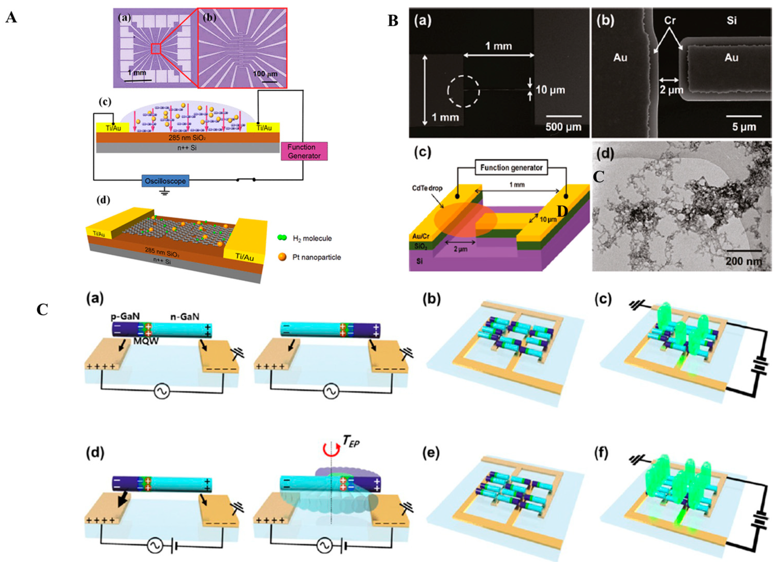
3.1. Metallic Nanostructures

Assembled NPs provide enhanced surface area, tunable optical properties, and have excellent electrical conductivity. Researchers have used them to create sensitive electrochemical sensors [88] or enhanced optical detection [89]. In particular, gold NPs (AuNPs) are extensively used in bio-applications due to their versatility and biocompatibility [90]. Therefore, several researchers have sought to utilize DEP as a tool to handle and/or assemble metallic NPs to enhance these applications. A summary of the relevant works is listed in Table 2.
A significant advancement in this field is the development of nanoribbons from AuNPs on mica substrates through DEP-assisted cold welding (Figure 2A) [91]. This technique leverages the manipulation of electric field parameters, such as a voltage ranging from 1 to 20 V and frequencies between 100 Hz and 10 MHz, to control nanostructure growth. Adjusting the frequency led to the transformation of lengthy, winding ribbons into shorter, thinner, and straighter forms, highlighting the precision achievable with DEP. Additionally, platinum NPs assembled on reduced graphene oxide formed nanohybrids that greatly enhanced the performance of gas sensors, showcasing the potential of hybrid structures to achieve superior sensitivity [92].
DEP’s potential is further demonstrated in the precise positioning of single NPs. AuNPs have been trapped in nanogaps to fabricate single-electron transistors [95]. These devices rely on Coulomb blockade behavior, observed at low temperatures, to achieve high-precision electronic functionalities. The ability to position individual particles with such accuracy highlights DEP’s role in advancing nanoscale electronic applications.
Beyond assembly, DEP has revolutionized surface-enhanced Raman scattering by enabling the creation of hotspots, regions of intense localized electric fields that amplify Raman signals [96]. For example, researchers arranged gold NPs into pearl chains with nanogaps, using an AC voltage of 10 Vpp at 1 MHz, to detect molecules like adenine at femtomolar concentrations [71]. Silver NPs have also been dynamically positioned to create controlled hotspots such as dendrite, facilitating the detection of proteins and chemical biomarkers such as dipicolinate [97], melamine, and cocaine [4]. This active control of interparticle spacing underscores DEP’s versatility in tailoring structures for specific applications.
DEP has been instrumental in advancing the functionalization of scanning probe tools, particularly in enhancing Raman signals. Researchers have successfully positioned NPs at the apex of atomic force microscope (AFM) tips, enabling applications such as tip-enhanced Raman spectroscopy [74]. By fine-tuning DEP parameters, including the voltage and frequency, a reliable attachment of NPs has been achieved, resulting in high signal-to-noise ratios during Raman measurements [85]. The gap distance between electrodes can play a significant role for signal enhancement as well, as shown in Figure 2D [94]. This method not only improves detection accuracy but also offers a consistent approach for developing sophisticated sensing tools.
DEP’s ability to create one-dimensional nanoparticle chains has opened new frontiers in nanoelectronics and sensing. Chains of metallic NPs, formed through DEP, exhibit unique properties that are useful in flexible electronics, granular conductors, and bioelectronic applications [5]. For instance, researchers have shown that voltage and current conditions can be tuned to assemble chains of 150 nm AuNPs, as shown in Figure 2B, revealing dependencies on electrode gap width and electric field strength [93]. These findings provide insights into the design of conductive pathways and functional components for next-generation devices.
The controlled aggregation of metallic NPs extends to applications in biosensing and chemical detection. Concentrating NPs onto nanostructured tips using DEP has proven effective for detecting low-abundance analytes [98]. For instance, gold NPs as small as 80 nm were successfully trapped by leveraging both their polarizability and the transport effects of Brownian motion [56,99]. These advancements have significant implications for heat-sensitive applications, where low voltages and high frequencies ensure effective trapping without thermal degradation.
In more complex assemblies, DEP has enabled multi-step processes for constructing hetero-nanostructures. A two-step DEP process was used to fabricate Au-ZnO nanostructures for ultraviolet light detection, where the attachment of AuNPs significantly enhanced the photodetector’s performance [10]. Furthermore, 3D metallic nanostructures, such as nanopillars and nanorings, were assembled by optimizing DEP parameters, achieving electrical properties equivalent to electroplated gold and showcasing strong plasmonic resonances [73]. The schematic of the fabrication of 3D nanostructures is shown in Figure 2C.
Table 2. Summary of research works in DEP of metallic nanostructures.
Serial
No.
NanoparticleElectric Field SignalElectrode InformationRef.
NP TypeSize (Diameter/Length)MaterialVoltageFrequencyMaterials TypesLength Scales (Gap/Length/Width/Height)
1Metal NPs20 nmAu1–20 V100 Hz–10 MHzAlParallel, arrowhead100 µm[91]
2Metal NPs5, 10, and 20 nmAu2–3 V1 MHzAuNanogap20 nm gap electrode[100]
3Metal NPs20–30 nmAu10 Vpp1 MHzTi/AuInterdigitated 1 µm/-/1 µm/5 nm, 200 nm[71]
4Metal NPs60 nmAg10 v20 MHzCr/AuGap electrode5 µm/-/-/50 nm, 150 nm[97]
5Metal NPs50 nmAg1–20 Vpp1 Hz–1 MHzCr/AuQuadrapole-/-/-/5 nm, 100 nm[4]
6Metal NPs40 nmAu10 Vpp1 MHzAuNanopore 20 µm gap/70 nm Dia/5 nm Au coating[94]
7Metal NPs15–100 nmAg/Au1–20 Vpp1 MHzAuNanoelectrode array80 nm/-/-/50 nm[74]
8Metal NPs40 nmAg7–8 V1–10 MHzAuSi Tips/Au -[85]
9Metal NPs40 nmAg16 Vpp2.5 MHzAu--/-/-/100 nm[101]
10Metal NPs2, 10, and 100 nmAu20 Vpp5 MHzSiC/SWCNTSNanotip540 ± 140 nm[98]
11Metal NPs35, 120 nmAu0.6–6 Vrms600 kHzCr/AgNanoprobe(150–500 nm in diameter, 2–150 µm in length)[56]
12Metal NPs150 nmAu1.9–15 Vrms100 kHzAuGap electrode10 µm/[93]
13Metal NPs60 nmAu0.7–2.5 V1 kHz–1 MHzAuRounded/Rectangular40–100 nm, 1 µm, 10 µm/-/-/100 nm[102]
14Metal NPs100 nm–200 µm Silver coated Silica100–600 V200 kHzAlNeedle-shaped electrode-[5]
15Metal NPs20 nmAu3 V10 kHz–1 MHzCr/PdTriangular planar electrode3 µm/-/-/10 nm, 70 nm[10]
16Metal NPs40 nmDNA coated Au2.5–2.8 V4 MHzTi/AuNanogap electrode13 nm/-/-/-[103]
17Metal NPs10 nmAu9–13 V1 kHz–1 MHzCr/AuTriangular planar electrode10 µm/-/-/20 nm, 120 nm[104]
18Metal NPs80, 100, 150 nmAu<10 Vpp1–5 MHzITOThin-film electrode20 µm/-/-/-[99]
19Metal NPs20 nmAu3 Vpp1 MHzCr/AuNanogap electrode200 nm/-/-/5 nm, 30 nm[95]
20Metal + nonmetal NPs5, 10, 22 nmAu, Cu, W, Al, Si, PSL12–20 Vpp30–70 kHzCr/AuParallel electrode-/-/-/2 nm, 120 nm[73]
21Metal NP + Ligands10 nmAu4 Vpp1 MHzTi/PdNanogap electrode50 nm/-/100 nm/10, 40 nm[105]
22Metal NPs15 nmPt5 V500 kHzAuMicrogap electrode-/-/-/4 µm [92]
23Metal NPs2–4 nmPd1–4 Vpp500 kHz–2 MHzTi/AuCoplanar electrode 4 µm/-/-/10, 200 nm[76]
DEP has emerged as a vital technique for controlling metallic NPs, driving advancements in the creation of nanostructures, as well as in sensing and electronic applications. Its precision in manipulating nanoparticle behavior has propelled both foundational research and real-world innovations across multiple disciplines. With ongoing efforts to refine DEP methods, the possibilities for utilizing metallic NPs in nanotechnology and similar areas are vast.

3.2. Non-Conducting Nanostructures

Non-conducting particles, as natural insulators, undergo dielectric polarization in an electric field. Due to their well-defined, uniform, and inert dielectric properties, they serve as model systems for developing, validating, and optimizing novel DEP architectures [106]. Their consistent dielectric behavior and commercial availability make them ideal candidates for the calibration and prototyping of sensors designed for biological applications [107]. Consequently, researchers have utilized DEP as a tool for manipulating non-conducting particles to overcome the limitations of the existing techniques, separation and sorting studies, quantitative force measurements, as well as simulation and modeling studies. A summary of the relevant research and its key details is presented in Table 3.
A novel experimental approach was developed to measure the DEP potential spectrum of colloidal NPs while minimizing the influence of particle shape and size. This method employed confocal laser scanning microscopy to quantify the time-averaged number-density distribution of particles under a DEP force field, enabling the determination of the frequency-dependent dipole coefficient and the crossover frequency for NPs ranging from 63 to 410 nm. By leveraging a statistical mechanics-based framework, this approach enhanced the analysis of DEP response functions and is particularly effective at frequencies below the crossover frequency, where existing methods have limitations to detect small DEP forces [108].
The ultra-high yield of single NPs was achieved by combining pDEP and nDEP forces to enable reversible attachment and detachment of NPs. A 100 nm Au NW electrode was used to manipulate 100 nm red fluorescent beads and 25 nm polyethylene-glycol-coated CdSe/Zn QDs [83]. Additionally, the combination of pDEP and nDEP (10 Vpp signal), with the positioning capabilities of an atomic force microscope (AFM), facilitated the precise patterning of 10–30 nm alumina particle arrays on a hexamethyldisilazane-coated indium tin oxide (ITO) glass substrate [109]. AFM-DEP was also utilized in assembling 200 nm polystyrene particles into lines, ellipsoids, and dots [110]. Furthermore, a coaxial AFM probe-DEP tweezer has found its application in the trapping and collection of 20 nm polystyrene and deoxyribonucleic acid (DNA) molecules in a highly conductive (160 mS/m) buffer and an nDEP force in low conductive buffers (6 mS/m) [111].
Ultra-fast fluorescence correlation spectroscopy was demonstrated as an accurate and rapid characterization technique for colloidal NPs (<50 nm), comparable to the double-layer length scale under varying AC field frequencies (5 kHz to 20 MHz) and a potential of 10 Vpp. Results revealed two crossover frequencies that strongly depended on particle size and medium conductivity. The fluorescence images of the same are shown in Figure 3A [72].
Ionic concentration-polarization (CP)-based biomolecule preconcentration was combined with DEP dynamic trapping for assessing the binding signal. This addressed the limitation of conventional CP-based biomolecule preconcentration methods which struggle to control the spatial overlap between the preconcentrated plug of biomolecules and surface immobilized antibodies. Biotin-conjugated polystyrene particles (0.8 µm) and fluorescein-tagged avidin D were used with ac AC field of 10 Vpp and 100 kHz applied across a DEP electrode array of 25 μm wide and 25 μm gap [115].
A single electrodeless polydimethylsiloxane device was described for both the mixing and de-mixing of 20 nm and 100 nm polystyrene particles, with driving forces generated by 500 V AC, 50 V DC voltages, and electrokinetic driving forces along the channel [116]. A similar approach, incorporating nano-constrictions, was employed for rapid nanoparticle and protein detection [117]. Moreover, programmable manipulation of polymethyl methacrylate (PMMA) with a DEP microfluidic device was achieved [78,118]. The approach of using electrodeless devices or the programmable manipulation of NPs allows for dynamic control over the particles as well as offering scalability for handling larger sample volumes and a higher throughput, making DEP usable for large-scale applications.
A DEP micropipette tip with an agarose gel plug was designed to isolate 200 nm polystyrene particles and high molecular weight DNA (hmw-DNA) to the pDEP high-field region, while 10 μm polystyrene microbeads were directed towards the nDEP low-field region with an AC field of 160 Vpp and 10 kHz [84]. The same group, along with researchers from University of California, focused on a more cost-effective alternative for microelectrode patterning for DEP trapping of polystyrene NPs and λ-DNA [119]. They also utilized DEP to rapidly isolate hmw-DNA and NPs to the pDEP high-field region and blood cells to the nDEP low-field region from 20 μL whole blood samples, without the need for preparation [120]. These studies contributed to making DEP-based separation techniques more efficient, cost-effective, and accessible, opening doors for broader applications in medical diagnostics.
An integrated microfluidic Raman system with curved electrodes was used to determine the suspended particle concentration of Tungsten trioxide and polystyrene NPs via DEP, creating both high and low particle concentrations [121]. The issue of a short trapping range in conventional plasmonic traps was addressed with DEP-assisted plasmonic trapping. In this method, long-range DEP forces drew 150 nm polystyrene particles closer to the plasmonic trap, increasing trapping efficiency by three times [122]. Molecular detection on a gold nanohole array surface was enhanced by utilizing DEP to overcome diffusion limitations, enabling real-time, label-free detection of bovine serum albumin (BSA) molecules at 1 pM concentration. Reversible trapping was also demonstrated by alternating the signal frequency between pDEP and nDEP. Figure 3B gives an illustration of the experiment, showing an SEM image of the fabricated nanohole array along with the simulations indicating the analyte molecules being attracted towards the edges of the nanohole due to strong electric field intensity gradient along the rim of nanohole [112]. Additionally, the epifluorescent microscope’s lack of sensitivity to low levels of analytes was overcome by combining it with a DEP microelectrode array, enabling the detection of DNA and 40 nm polystyrene particles [123].
DEP was used to immobilize polystyrene NPs on electrode array tips. The combination of SEM and fluorescence intensity distribution facilitated the quantification of immobilized particles and the determination of the electrode-to-particle diameter ratio for single-particle immobilization [124]. To reduce surface roughness and enhance the trapping efficiency in traditional tips, a template-stripped gold pyramid was fabricated using a conductive and dielectric epoxy mix, and the fabrication process along with the SEM images of the gold-pyramid are shown in Figure 3C. This gold pyramid, combined with an ITO electrode, served as a movable DEP trap capable of trapping 2 μm and 190 nm polystyrene particles, as well as single-walled CNTs [113].
A high-throughput DEP-based filtration technique was demonstrated, enabling selective trapping and efficient recovery of microparticles in the mL/min flow range, with scalability up to 50 L/min by increasing the filter cross-section. Compared to conventional microfluidic DEP devices, the technique achieved a five-orders-of-magnitude increase in throughput while maintaining high selectivity. Additionally, the method demonstrated high reusability, achieving 86–92% recovery rates with pH adjustments. These findings validate the feasibility of DEP filtration in macroscopic porous materials, offering a scalable solution for high-throughput particle separation [125].
A scalable and reproducible DEP-based assembly technique was developed for printing nanostructures with precise dimensional control. By applying an alternating current (AC) field and a direct current (DC) offset voltage, NPs were directed into patterned vias, achieving high-uniformity assembly. The combination of 3D-DEP and electrophoresis generated sufficient forces to assemble silica nanorods (20–200 nm diameter, 500 nm–2 μm spacing) and hybrid silica/gold nanorods for plasmonic applications. Compared to conventional approaches, DEP-driven assembly offers a high-precision, bottom-up, and scalable approach for nanoelectronics, photonics, and biosensing. These findings establish DEP as a powerful platform for nanoscale printing, enabling large-area, high-resolution nanomanufacturing [126].
Novel lab-on-a-chip technology integrated droplet microfluidics with DEP to fabricate uniform H1-DNA polyplexes-based nanomedicine. The biological experiments showed that the DEP-treated NPs maintained their gene transfection capability and exhibited significantly higher transfection efficiency (15%) compared to the control group (4%) in HUVEC cells. DEP improved drug delivery efficiency, streamlined the fabrication, mixing, and separation of NPs, and reduced the processing time (from 10 min to 1 min) associated with droplet microfluidics [127].
A recent study investigated methods to generate a high-electric-field gradient to overcome the Brownian transport of NPs and enable bulk electrokinetic particle trapping. A carbon nanofiber mat sandwiched between copper tapes was used as an electrode, with an ITO slide as a planar electrode. A maximum gradient field-squared of 2.82 × 10¹⁷ V2/m3 was simulated around the fiber edges enough to trap 20 nm particles. Polystyrene particles of various sizes (20 nm, 210 nm and 1 µm) were successfully trapped with an applied electric potential of 7 Vrms, and the SEM images in Figure 3D show the trapped particles around the fiber edges as predicted by the simulations [86].
A cost-effective novel approach was adopted to amplify the localized AC electric field by two orders of magnitude, enabling the rapid trapping of 20 nm colloids and bacteria from a diluted blood sample [128]. Sub-10 nm gaps were created between gold electrodes, promoting the rapid, long-range DEP trapping of 30 nm polystyrene, 40 nm diamond, and 8 nm CdSe QDs with a bias voltage as low as 200 mV. By shrinking the separation between gold electrodes to sub-10 nm using high-throughput atomic layer lithography, instead of e-beam lithography, strong trapping forces over a mm-scale trapping zone were created. The illustration of the nanogaps along with the particle trapping are shown as fluorescence images and SEM images in Figure 3E [114].
A novel statistical image quantifying method was developed to determine nanoparticle electrokinetic parameters. It was compared with traditional methods using 200 nm latex nanospheres in low-conductivity media and a planar castellated electrode array for pDEP [129]. Exploiting the innate differences in dielectric properties of NPs, low-density non-magnetic drug delivery NPs (liposome-based, polymer-based, and hollow silica shell-based) with stealth surface coating were recovered from undiluted human plasma [130]. The selective manipulation of 100 nm polystyrene and 20 nm quantum dot NPs in three degrees of freedom was achieved at gold nanostructures fabricated between electrodes, using the floating AC-DEP force with 8 Vpp [131]. Furthermore, assembly of the poly-L-lysine core–shell NPs of 220 nm and 400 nm was accomplished with the assistance of DEP [132].
A novel microfluidic chip with zig-zag/face-to-face electrodes for AC and parallel electrodes for DC was devised to establish a continuous upconcentration flow system for sub-100 nm particles. It successfully achieved upconcentration by a factor of 11 for particles as low as 47 nm at 2 µL/h [133]. The capture efficiency of single particle passage through a 1.4 µm micropore was enhanced by controlling the traffic of a polystyrene particle (780 nm) with AC-DEP (2–10 MHz) [134].
Table 3. Summary of research works in DEP of non-conducting nanostructures.
Serial
No.
NanoparticleElectric Field SignalElectrode InformationRef.
NP TypeSizeMaterialVoltageFrequencyMaterials TypesLength Scales (Gap/Length/Width/Height)
1NPs63, 160, 200, and 410 nmpolystyrene 10 Vpp30 MHzAu/CrCoplanar parallel electrodes27 µm/22 mm/-/0.2 µm[108]
2NPs/
QDs
100, 25 nmPolystyrene/PEG coated CdSe/Zn QDs8 Vpp3 MHz–50 MHzAuNanowire electrodes10 µm/-/100 nm/-[83]
3NPs10–30 nmAluminum oxide10 Vpp1 kHz–10 MHz ITOPlanar electrodes(4 mm × 4 mm reservoir)/1 cm/1 cm/1 mm[109]
4NPs20 nm, 210 nm, and 1 µmpolystyrene 7 Vrms1 kHz–1 MHzCarbon nanofiber mat/ITOElectrospun nanofiber electrode150 µm gap/Mat–80 µm thick and 3 mm wide [86]
5NPs10–50 nmpolystyrene10 Vpp5 kHz–20 MHzAuQuadrupole microelectrodes20 µm gap/-/-/-[72]
6NPs/DNA molecules20, 10 nmpolystyrene2 Vrms100 kHz–50 MHzAu/CrCo-axial probe electrodes-[111]
7NPs0.8 µmbiotin/avidin-conjugated polystyrene10 Vpp80–100 kHzAu Interdigitated electrode 25 μm/-/25 μm gap/-[115]
8NPs20, 100 nmpolystyrene500 V600 Hz-Electrodeless-[116]
9NPs/
DNAmolecules
200 nm, 10 µmpolystyrene/genomic hmw-DNA160 Vpp/80 Vpp10 kHz/3 kHzPt/AuNanowire electrode/ring type counter electrode-[84]
10NPs220, 80 nmPolystyrene/
tungsten trioxide
15 V250 kHz–20 MHzAu/CrCurved electrodes20–80 nm/270 nm/30 nm/200 nm [121]
11NPs150 nmPolystyrene0.18 V/µm10 kHzAu/ITONanopillar electrode120 nm height/150 nm radius[122]
12NPs/
Bioparticles
190 nmPolystyrene/BSA10 Vpp/6 Vpp1 kHz–10 MHzAu/ITONanohole array/planar electrodeHole diameter—140 nm/periodicity—600 nm[112]
13NPs100 nm to 2 µmPolystyrene1.7 to 13.7 Vrms15 kHzW, Si/ITOVertical and conical array/planar electrodeGap—2 µm/W—500 nm dia, Si—50 nm dia./Height—40 nm[124]
14NPs/DNA molecules40 nmpolystyrene/DNA20 Vpp10 kHzPtMicroarray electrodes80 µm dia/Dimensions—2 mm × 2 mm[120]
15NPs/
DNA molecules
200 nmpolystyrene/
λ-DNA
12 Vpp6 kHzAu/NiInterdigitated circular electrodes100 µm/-/-/3 to 5 µm[119]
16NPs5, 20, 40, and 80 nmSi/Au12 V1 MHz/10 MHzAu, PMMA/Au Planar electrodes-/-/-/235 nm[126]
17Polymer/DNA116 nmH1/DNA plasmids8 Vpp20 MHz-Interdigitated electrodes-[127]
18Micro/NPs0.5, 3, and 4.5 µmPolystyrene/Graphite150–600 Vrms1 kHz–15 kHzStainless steel Parallel planar electrodes8 mm/18 mm/8 mm/29 mm [125]
19NPs190 nm, 2 µm, Polystyrene10 Vpp10 kHz–10 MHzAu/ITOPyramid tip/Planar electrode70 µm/-/-/-[113]
20NPs/
DNA molecules
40 nmpolystyrene/DNA20 Vpp/14 Vpp10 kHzPtMicroarray electrodes80 µm dia, Patch dimensions—200 µm[123]
21NPs300 nmPMMA10 Vpp200 kHzAu/ITO Fish-bone type/Planar electrode50 µm/-/30 µm/-[118]
22NPs 300 nmPMMA10 Vpp200 kHzAu/ITO Planar electrode30 µm/2000 µm/30 µm/- [78]
23NPs50 nm/40 nm/50 nmAnti-FITC/polystyrene/Au50/100/300 V50/500/260 kHzSi Electrodeless150 nm/-/-/-[117]
24NPs/Bacteria5 µm and 20 nmPolystyrene/Staphylococcus aureus and Pseudomonas aeruginosa15 Vpp100 kHz–1.2 MHzAu/TiQuadruple electrode array-/-/-/235 nm[128]
25NPs200 nmPolystyrene1 V1–4 MHzPtCastellated arrays5 µm/-/5 µm/100 nm[129]
26Polymer/nanomedicine particles100–200 nmPolymer, Silica, Liposome18 Vpp,15 Vpp, 8 Vpp, 12 Vpp15 kHzPtCircular electrode array60 µm diameter[130]
27NPs/
QDs
100, 20 nmPolystyrene/QDs8 Vpp1 MHzTi/AuMicroelectrode10 µm/-/-/55 nm[131]
28Core–shell NP220 and 400 nmpoly-L-lysine shell NPs5 Vpp1 kHz–80 MHzTi/AuQuadrupole microelectrodes25 µm/-/-/100 nm[132]
29NPs/Bioparticles200 nmPolystyrene/BSA10 Vpp10 kHzplatinum−iridium/ITOTip and Planar electrodeTip: Size—20 nm, height—15 nm, length—225 μm[110]
30NPs47 nm, 1 µmPolystyrene20 Vpp10 kHz–1 MHzTi/AuZig-zag/face-to-face Placement angle—60°. Zig-Zag gap—6 µm. Face-to-face gap—5 µm. Height—110 nm[133]
31NPs780 nmPolystyrene1 V2 MHz–10 MHzPtCrosswise configuration1 µm/-/-/60 nm[134]
32NPs/
QDs/nanodiamond
30, 10, 190 nmPolystyrene/Nanodiamond300 mV/750 mV/400 mV to 600 mV1 MHz to 10 MHz/1 MHz/100 kHzAuNanogap electrode1–10 nm/0.8 mm/20 µm/150 nm[114]
DEP has emerged as a powerful tool for manipulating non-conducting particles, enabling researchers to develop innovative techniques and improve existing technologies. The integration of DEP with traditional approaches has led to breakthroughs, overcoming previous limitations and yielding unexpected results. Additionally, novel statistical methods for analyzing electrokinetic parameters have enhanced image quantification and data analysis. The unique properties of non-conducting particles make DEP invaluable for applications such as calibrating and validating biological sensors, separation and sorting, quantitative force measurements, and simulation studies. As research continues to advance, DEP will likely play an even greater role in shaping the future of electrokinetic manipulation of non-conducting particles.

3.3. Nanowires/Nanotubes/Nanorings and Similar

The ability to control the alignment and assembly of one-dimensional nanostructures such as NWs, nanotubes (NTs), and nanorings (NRs) is central to their integration into functional devices. DEP’s versatility in controlling the positioning, alignment, and functionalization of such nanomaterials has made it indispensable for applications across disciplines. Researchers have used them in fabricating flexible electronics including display devices, transistors, memories and logic gates, solar cells, sensors, and nanogenerators [135]; in energy conversion devices [136]; multicolor nanophotonics [137], etc. Here, we review key studies on the assembly, patterning, and sensor integration of NWs, NTs, and NRs through DEP, highlighting recent advancements and the diversity of approaches within this domain. A summary of relevant research is shown in Table 4.
Before exploring the direct applications of DEP in the assembly and patterning of NWs and NTs, exploring several key factors, including frequency, electrode design, and medium properties, is essential. Several studies have highlighted the intricate relationship between the applied frequency, material properties, and assembly behavior, offering valuable insights into the conditions required for controlled nanostructure manipulation.
For instance, Kataoka et al. demonstrated that tuning the frequency (10 kHz to 1 MHz) significantly impacts the rate and quality of Ag NW assembly, optimizing their alignment for specific applications [138]. Similarly, a study using a 3DEP chip showed that higher frequencies (above 1 MHz) improved the conductivity of aligned NWs, suggesting frequency control enhances both assembly and electrical performance [139]. Tao et al. found that the alignment of ZnO NWs and carbon NTs is governed by the combined effects of frequency and electrode gap size, which are crucial for integrating nanostructures into functional devices [140]. Additionally, Abdulhameed et al. explored how medium properties, such as permittivity and conductivity, influence CNT motion during DEP, offering insights for optimizing the process in different environments [141]. Duchamp et al. found that the dielectric permittivity of the solvation shell of CNTs and the pattern of the electric field, determined by the substrate resistivity, lead to differences in the results of DEP. Solvents with a low solvation shell dielectric constant (water and isopropyl alcohol) should be used to separate conducting CNTs, as shown in Figure 4A [142]. These studies underline the importance of precise DEP control for effective NW and NT assembly in device applications.
DEP has enabled the precise assembly and positioning of NWs and NTs for a variety of applications. Studies have demonstrated that by adjusting the frequency and voltage, Ag NWs can be directed between electrode pads or along their edges, which is useful for NW-based sensors and interconnectors [146]. Additionally, a self-limiting DEP process has been developed to achieve 98.5% precision in single-NW assembly, essential for large-scale production of NW-based devices [147]. Cao et al. further advanced the technique by using fringing electric fields to align high-density CNT arrays with a consistent pitch of 50 NTs per micrometer, enabling their application in high-performance nanodevices like field-effect transistors [11]. Furthermore, combining DEP with capillary-assisted assembly allows for precise alignment and secure positioning of NWs, enhancing scalability for flexible electronics [148].
Building on these advancements, Wang et al. developed a reusable electrode method for assembling Ag NWs on flexible PET substrates using sinusoidal AC voltages, achieving ordered arrays and rectangular mesh-like networks through a two-step field rotation, demonstrating potential for low-cost integration in flexible electronics [149]. Similarly, a study on NW-based oscillators employed DEP and magnetic interactions to precisely anchor multisegmented NWs on patterned nanomagnets, enabling synchronized motion for thousands of cycles, with applications in nano-resonators and biochemical sensing [150]. Additionally, a scalable DEP technique for site-selective nanoparticle trapping incorporated capacitors to limit multiple particle trapping, achieving a 70% single-particle yield and offering a precise, scalable solution for nanostructure assembly in large-scale device fabrication [143]. As shown in Figure 4B, the design incorporated a capacitor in series with the electrodes. The impedance between the electrodes is reduced when an NW bridges the gap and the capacitor takes the majority of applied potential, thereby reducing the voltage across the gap and inhibiting multiple particles from being trapped.
The optimization of CNT positioning has also been explored, with research showing that solvent polarity and substrate characteristics play a crucial role in their alignment during DEP, which could improve CNT-based sensors and electronics [151]. Additionally, a study on the charge transport behavior of single CuO NWs revealed their potential for use in sensors and optoelectronics, where understanding the charge transport is critical to device performance [152]. A universal set of parameters for aligning NWs, applicable to various materials, is determined, focusing on factors such as peak-to-peak potential, frequency, the thickness of the silicon oxide layer, grounding of the silicon substrate, and solvent properties for templated cathodic electrodeposition [153]. These studies highlight the versatility of DEP in the assembly and functional integration of NWs and NTs, paving the way for their use in advanced electronic and sensor technologies.
Patterning NWs, NTs, and NRs is crucial for integrating nanostructures into functional devices, and DEP offers an efficient, scalable solution. One method utilizes surface acoustic waves to tune the frequency and assemble NWs into specific geometric patterns, providing a contactless, template-free approach suitable for large-area patterning [144]. A schematic representation of formed patterns is shown in Figure 4C. Another study used DEP to position gold NWs around patterned cylindrical posts, with frequency adjustments allowing for the selective placement of NWs between or around the posts. This reconfigurable technique enables the creation of complex patterns for optical and nanoscale applications [154]. Additionally, a DEP system with dot-matrix electrodes was developed for precise NW alignment, improving capture rates and positioning, making it effective for integrating NWs into electronic devices with varying lengths [155]. Different assembly patterns and controls of the pattern can be achieved by varying the electric field voltage and frequency. These studies highlight the versatility of DEP in creating well-defined patterns essential for advancing nanodevice technologies.
NWs, NTs, and NRs are ideal for sensor applications due to their high surface-to-volume ratio and tunable electrical properties, with DEP enabling their precise assembly into functional sensors. One study integrated CNT sensors into CMOS microsystems, creating an array of individually addressable CNT-based sensors with high sensitivity to pH changes, showcasing DEP’s potential for environmental monitoring and biotechnology applications [156]. This excellent review focused on gas and photosensors, where DEP was used to assemble semiconducting NWs and CNTs with exceptional sensitivity and reproducibility, highlighting DEP’s versatility in sensor fabrication [157].
In addition to enabling assembly and patterning, DEP also allows for the real-time manipulation and in situ characterization of individual nanostructures, offering valuable insights into their behavior and performance. One study demonstrated the manipulation of SnO₂ nanobelts in a microfluidic environment using AC DEP, where pDEP and nDEP forces were used to control the movement of the nanobelts, suggesting new applications in sensors and optoelectronics [158]. Similarly, real-time manipulation of Si NWs was achieved with DEP, with I-V measurements and photoconductivity analysis providing insights into their potential integration into electronic and photonic devices [159]. The movement of catalytic nanomotors can be controlled using a combination of DC field to modulate the speed through electrophoretic and electroosmotic forces while the AC field guides their alignment through an induced dipole, as shown in Figure 4D, which has the potential of powering functional nanomechanical devices [145]. Additionally, the DEP growth of platinum NWs was studied, focusing on the effects of concentration and temperature on their growth, further enhancing the understanding of how DEP can be leveraged for NW-based device fabrication [77]. Together, these studies highlight the crucial role of DEP not only in assembling nanostructures but also in enabling their precise manipulation and characterization for advanced applications.
DEP continues to demonstrate its pivotal role in advancing the fabrication, assembly, and manipulation of one-dimensional nanostructures such as NWs, NTs, and NRs. Through its diverse applications—from patterned assembly for device integration to the development of advanced sensors—DEP offers a scalable, versatile solution for the fabrication of next-generation nanomaterial-based devices. As techniques like surface acoustic wave-assisted patterning, fringing-field assembly, and self-limiting deposition continue to evolve, the potential for DEP in nanomanufacturing will only expand, enabling breakthroughs in electronics, biotechnology, and nanorobotics.
Table 4. Summary of research works in DEP of nanotubes/nanorings/nanowires and similar.
Serial
No.
NanoparticleElectric Field SignalElectrode InformationRef.
NP TypeSize (Diameter/Length)MaterialVoltageFrequencyMaterialsTypesLength Scales
(Gap/Length/Width/Height)
1Metal NPs/NWs100 nm (NPs), 60 nm (NWs)Ag10–30 Vpp10 kHz–1 MHzITOInterdigitated, pillars, and pits-[138]
2NWs/NTs200 nm/3 µmZnO, CNT5 V1 MHzTi/AuNarrow gap1 µm, 4 µm, 5 µm/-/-/5 nm, 30 nm[140]
3sc-SWCNTs-CNT10 V500 kHzITORectangular gap electrode10 µm/995 µm/-/0.14 µm[141]
4MWCNTs/NWs5 nm/200 nm–4 µmZnO/TiO2/VOX/CNT2 V1 MHzAuMicroelectrode pair2 µm/-/-/50 nm[142]
5NWs220 nm/30 µmCuO6 V20 kHzAuGap electrode2.25 µm/-/-/-[152]
6NWs60 nm/40 µmAg-19–37 MHzCr/AuGap electrode75 µm/-/75 µm/50 Å, 500 Å)[144]
7NWs300 nm/2.5 µmSiO2 coated Ag2–6 V750 kHzTi/AuCylindrical post-/-/-/15 nm, 30 nm[154]
8NWs100 nm/200 µmAg0.6–5 V10 kHz–10 MHzAgDot-matrix electrode50 µm diameter/150 µm gap[155]
9NWs75 nm/22 µmSi10 Vpp1 kHz–20 MHzAu3D-well electrode150 µm/-/-/70 Cu, 150 Polyamide[139]
10NWs2 nm/-Au2–10 Vpp2–20 MHzCr/AuParallel probe electrode3 µm/5 nm, 50 nm[146]
11NWs30 nm/20, 60 µmAg5–70 Vpp1 MHz Interdigitated electrode36, 65 µm/-/36, 184 µm/-[149]
12SWCNT-/600 nmCNT5 Vpp400 kHzTi/Pd/AuSurface microelectrodes100 nm/-/100 nm/0.2, 15, 15 nm[11]
13NWs50 nm/4–5 µmSi/InAs/ZnO3.2 Vpp50 kHzCrInterdigitated electrode2, 4, and 5 µm/-/-/100 nm[148]
14NWs30 nm/1–20 µmSi5–20 Vpp5 kHz–5 MHzTi/AuParallel electrode-bars/Interdigitated electrode10, 20 µm/-/-/2 nm, 50 nm[151]
15NWs240 nm/18 µmSi7 Vrms500 HzAlIsolated and sparse electrode-/12 µm/2 µm/50 nm[147]
16NWs151 nm/5.8 µmAu2–8 Vpp10–50 MHzAu/Ni/AuQuadrupole microelectrode-/-/-/6 nm, 100 nm, 100 nm[150]
17NWs-Au/MWCNT4 Vpp10 kHz–1 MHzCr/AuArray of electrodes100 nm/-/150 nm/85 nm[143]
18NWs130 nm/-Si0.3–5 V1 MHzTiTapered electrode4 µm/-/-/-[159]
19Nanobelt1–2 µm length/sizeSnO270 Vpp5 Hz–10 MHzAuCastellated microelectrodes20 µm/-/-/250 nm[158]
20Nanomotor250 nm/5 µmPt–Au0–50 Vpp10 kHz–10 MHzAuQuadruple microelectrode-/-/-/500 µm[145]
21NWs/NTs50–150 nm/4–6 µmNi, ZnO, Au, Ag, Sn, Fe2O30.6–6 Vpp50–200 kHzAuParallel plate electrodes-/-/-/400 nm[153]
22NWs23 nm/-Pt4 V100 kHzPt/AuInterdigitated electrode2–4 µm/-/-/3, 17 nm[77]
23NTs1–3 nm/CNT5–20 Vpp300 kHzW-Ti/PtInterdigitated electrode-/-/-/120 nm[156]

3.4. Other Semiconductive Nanostructures

Other semiconductive nanomaterials like graphene, carbon black, quantum dots, indium gallium nitride, etc., have emerging applications due to their unique electronic, optical, thermal, and chemical characteristics. Researchers have used them to create novel biosensors [160], sensors for environmental contaminants monitoring [161], and in high performance photodetectors [162]. In particular, graphene-based semiconductive nanomaterials have great potential in optical and optoelectronic applications, including light-emitting devices, photovoltaics, saturable absorbers for ultra-fast lasers, transparent conductive electrodes, photodetectors, and phototransistors, as well as new and developing photocatalytic applications and biological processes [163]. As a result, researchers utilized DEP to assemble, manipulate, and precisely align such nanostructures to facilitate these applications. A summary of relevant research with key parameters has been listed in Table 5.
DEP is an effective technique for assembling and manipulating nanostructures with properties suited to advanced sensing, particularly hydrogen detection. Through precise control of voltage, frequency, and processing time, DEP enables the assembly of Pt-decorated graphene oxide (GO) nanostructures between microgap electrodes, achieving around 10% sensitivity at 200 ppm hydrogen at room temperature, making it ideal for applications like gas storage and leak detection [164]. The optical microscope image of the fabricated microgap electrodes and the schematic of the experimental system are demonstrated in Figure 5A. Similarly, a high-performance hydrogen sensor using reduced graphene oxide decorated with Pt–Pd NPs has been developed, exhibiting stable and repeatable responses due to mechanisms like carrier donation and lattice expansion [165]. Enhanced by factors like nitrogen as a carrier gas, DEP-assembled sensors demonstrate adaptable and efficient hydrogen detection across varied environments, highlighting DEP’s versatility in creating responsive, high-performance sensors for diverse applications.
DEP has also been applied to precisely align SrTiO3 NPs between microelectrodes, enabling electrical measurements that reveal conduction mechanisms, such as hopping and tunneling, dependent on temperature [168]. This setup emphasizes DEP’s utility in forming semiconductive nanostructures with specific electronic properties. Similarly, self-assembly capabilities in DEP have facilitated the formation of photoconductive microbridges using CdTe NPs [166]. The DEP electrode along with the experimental setup and TEM images of NPs dispersion after DEP where particles formed chain are shown in Figure 5B. These size-quantized particles self-organize into chains, amplifying polarization volume and allowing low-voltage assembly while retaining optical properties. The organized NP chain structure opens avenues for MEMS, optoelectronic devices, and sensors.
DEP’s flexibility extends to assembling large-scale devices, as seen with green InGaN nanorod LEDs [169]. Combining techniques such as nanosphere lithography and DEP, millions of nanorod LEDs are arranged between interdigitated electrodes over large areas, achieving scalable, polarized lighting. The devices, though under development, show potential for high-luminance applications like displays. An advanced DEP method using DC-offset AC and pulsed-DC electric fields further enhances this potential by achieving 1.8-times greater electroluminescence intensity than conventional AC-DEP [167]. The schematic of the aligned nanorod orientation is shown in Figure 5C. The pulsed-DC field significantly improves nanorod alignment, leading to increased brightness and current under DC operation, which is promising for a high-efficiency, scalable surface and formable lighting. DEP has also proven effective in fabricating ZnO NP-based ultraviolet sensor arrays with low operating voltage and robust environmental stability [170]. This capability highlights DEP’s potential for developing sensitive, low-power photodetectors across various applications.
Innovative uses of DEP also include growing carbon black wires in acrylate monomers, where voltage, frequency, and temperature impact wire growth and shape, transitioning from linear to fractal structures at higher frequencies [171]. This approach holds promise for creating conductive adhesives suitable for semiconductor packaging. Additionally, carboxylic-functionalized CNTs have been suspended and arranged into controlled gap networks between parallel electrodes, aided by NT interactions in DEP setups [172]. The successful alignment of CNTs showcases DEP’s potential in forming conductive nanostructures with custom geometries for electrical applications.
Beyond assembly, DEP has enabled the precise trapping and manipulation of onion-like carbon (OLC), or carbon nano-onions, which show promise for sensors and nanoelectronics [173]. By optimizing electric field parameters, OLCs are efficiently positioned between microelectrodes, showcasing DEP’s adaptability. Integrating DEP with Raman spectroscopy has further enabled in situ analysis of suspended particles like WO3 NPs [121,174]. DEP concentrates particles within specific regions, enhancing Raman analysis of type and concentration, a technique with broad potential for biosensing and particle interaction studies.
DEP’s versatility extends to optofluidic, where it modulates optical properties by controlling nanoparticle distributions near waveguides, impacting light transmission. Electric field tuning positions particles like tungsten trioxide and silica around waveguides, a method paving the way for responsive optofluidic sensors [175]. Another approach combines DEP with ACEO to position QDs on nanowire arrays [176], enhancing biosensor sensitivity by targeting bioanalytes. DEP’s capacity for fine particle control opens opportunities for QD-based biosensors with improved detection.
In NP sorting, DEP has shown effectiveness in separating ZnO particles by shape under low-frequency AC fields [177], achieving distinct placements of rods and cubic forms in an acetone suspension. This precision sorting technique could benefit nanoparticle purification processes, while DEP’s phase-separating ability in graphene oxide dispersions supports microstructure engineering for optical applications [178]. Additionally, DEP’s selectivity based on dielectric properties is utilized in an electrokinetic platform to recover drug-delivery NPs from plasma [130]. This platform preserves plasma protein integrity, enabling the isolation and further analysis of particles. Such a method provides a new avenue for assessing NP stability within biological systems, which is invaluable in drug delivery research.
Through its diverse applications, DEP showcases its transformative potential in creating semiconductive nanomaterial-based sensors and devices with customizable properties, making them ideal for a variety of advanced sensing applications. For more studies and a broader perspective, readers are encouraged to read the following review study which emphasizes the effectiveness of DEP as a bottom-up approach for fabricating nanomaterial-based sensors [157].
Table 5. Summary of research works in DEP of other semiconductive nanostructures.
Serial
No.
NanoparticleElectric Field SignalElectrode InformationRef.
TypeSize (Diameter/Length)MaterialVoltageFrequencyMaterials TypesLength scales(Gap/Length/Width/Height)
1Nanostructure + NPs1 nm GO/15 nm PtGraphene Oxide/Platinum2, 5, and 10 Vpp100, 500, 1000 kHzTi/AuMicrogap electrode 4 µm/-/-/-[164]
2Nano-onions5 nmCarbon3–20 Vpp1, 100, and 1000 kHzAuInterdigitated microelectrode5 µm/6760 µm/5 µm/-[173]
3NPs21.4 nmStrontium titanate5 V1 MHzAlProbe electrodes100 nm/-/-/60 nm[168]
4NPs80 nm& 210 nmTungsten trioxide and Polystyrene15 V100 kHz–20 MHzCr/AuCurved microelectrode-/-/-/50, 100 nm[121]
5Nps4.2 nm/-Cadmium telluride4–10 V100 kHzCr/AuMicrogap electrode 2 µm/-/-/-[166]
6Nanorods500 nm/2.5 µmIndium gallium nitride/Gallium nitride 2.8–21 Vrms 100–950 kHzAuInterdigitated microelectrode2.5 µm/-/3 µm/-[169]
7NPs20–100 nmZinc oxide 10 V300 kHzTi/PdGap electrode 800 nm/200 nm/45 nm/5, 40 nm[170]
8CBNPs30 nm/-Carbon black 12–225 V10 Hz–10 kHzCuTriangular planar electrode2–30 mm/-/-/88 µm[171]
9MWCNTs40–60 nm/5–15 µmMultiwall carbon nanotube 20 Vpp5 MHzCr/AuParallel electrode 1–10 µm/10 mm/5 mm/30, 100 nm[172]
10Nanorods 500 nm/3 µmIndium gallium nitride/Gallium nitride 21 Vrms950 kHzTi/AuInterdigitated microelectrode3 µm/0.7 cm/0.6 cm/20, 200 nm[167]
11NPs 300 nm/15 µmZinc oxide 40 Vrms 1 kHzAuIn-plane electrode 150 µm/-/-/-[177]
12NPs 1 nm/5.69 µmGraphene Oxide20 Vpp10 kHzITOInterlaced electrode1 mm/-/1 mm/-[178]
13NPs 450 nm, 80 nm/-silica and tungsten trioxide15 Vpp0.1–250 MHzCr/AuCurved microelectrode 20 µm/17 mm/-/-[175]
14NPs 60 nm, 109 nm, 10–20 nm/10 nmPolystyrene/Nanoliposomes/Micelles/DNA strands2–18 Vpp15 kHzPtMicroelectrode 218 µm gap/60 µm diameter[130]
15NPs 10 nm QD/300 nm, 5 µm Au NanowiresCadmium Selenide, Zinc Sulfide QDs/Gold NWs20 Vpp50–700 kHz-Parallel microelectrode 20–50 µm/-/-/-[176]
16NPs 3–8 nmPlatinum-palladium 10 Vpp1 MHzTi/AuTriangular probe electrodes2 µm/-/-/5 nm, 90 nm[165]

4. Discussion and Conclusions

This review focuses on the DEP phenomena of NPs, providing a theoretical foundation to understand the processes and challenges occurring at the nanoscale, including the need for high field gradients to overcome Brownian motion and the presence of electrohydrodynamics. This article summarizes the recent developments and applications of NP DEP platforms over the past 15 years, a period characterized by exciting challenges and advancements in the manipulation and separation of increasingly smaller objects using DEP. With the current trend in DEP research, as illustrated in Figure 1, this focused review aims to guide researchers towards areas that warrant the most attention for future practical applications. Over the years, the field has made significant progress, pushing the boundaries of unique developments and applications in this area.
DEP is a highly effective technique for manipulating NPs within microfluidic systems. It enables precise sorting, trapping, transportation, and characterization of NPs. Additionally, DEP plays a significant role in the fabrication of electronic and optical devices by utilizing NPs as fundamental components. The technique also allows for the systematic arrangement of particle arrays in specific patterns and positions, enhancing their application in nanotechnology. By incorporating these fundamental developments, DEP has substantial potential in the biomedical field, particularly in handling small biological entities such as DNA, viruses, vesicles, supramolecular structures, molecules, bacteria, and proteins.
By providing precise control at the nanoscale, DEP opens new avenues for research and innovation, addressing scientific challenges that conventional methods struggle to resolve. For example, DEP is increasingly recognized as a powerful and emerging tool in biomedical research, particularly in areas like liquid biopsy and antimicrobial resistance (AMR) diagnostics. In liquid biopsy, DEP can separate critical disease markers, such as circulating tumor cells and extracellular vesicles, from complex biological fluids without requiring labels, making it valuable for early-stage cancer detection and non-invasive patient monitoring [179,180]. In the context of AMR, DEP enables the rapid sorting of live and dead bacterial populations by exploiting their distinct dielectric properties, offering a quicker and more direct alternative to conventional antibiotic susceptibility testing [181,182]. Moreover, though proteins were long considered too small to be influenced by DEP, research by Hölzel and Pethig [183] showed that under specific conditions—namely, when suspended in low-conductivity solutions like deionized water and subjected to high-frequency, non-uniform electric fields in the megahertz range—proteins do exhibit DEP movement. These insights open new possibilities for DEP in protein analysis, expanding its relevance in diagnostics and point-of-care technologies [184]. These technological trends and emerging directions in AC-DEP applications within microfluidics offer readers a clearer vision of where the field is heading.
Controlling NPs using DEP requires precise management of electric field gradients. While DEP technology for various micro-sized particles is well established, its effectiveness with sub-micron and nano-sized particles is still developing and requires significant attention for practical applications. This limitation arises from the cubic nature of the DEP force relative to particle size; consequently, a much stronger force is needed to manipulate smaller particles. A strong electric field, combined with a conductive medium, can lead to temperature increases within the system. This rise in temperature can result in electrolysis and electrode deterioration, which may compromise the system’s efficacy. Therefore, the careful design of electrodes and flow channels is essential to create significant localized field gradients capable of handling nano-sized particles. Such designs would allow for moderate voltages to be applied without a substantial increase in temperature, thereby enhancing the effectiveness of nanoparticle manipulation, separation, trapping, and enrichment. Fortunately, advancements in nanofabrication are facilitating the meticulous design of electrodes and flow channels [69]. However, they use nanofabrication techniques to design high-resolution electrodes, which are sometimes costly and challenging to scale for mass manufacturing [68]. Research is progressing towards overcoming the challenges associated with DEP for NPs.
The efficiency and selectivity of AC-DEP are strongly governed by the frequency of the applied electric field, as different particles exhibit unique dielectric behaviors across frequency ranges [185]. For instance, gold nanoparticles (AuNPs) showed significant changes in assembly morphology when the frequency was varied from 100 Hz to 10 MHz, with higher frequencies producing straighter, more compact nanoribbons [91]. Similarly, in nanowire (NW) assembly, lower frequencies increased the rate of alignment, while frequencies above 1 MHz enhanced conductivity and structural integrity [138,139]. These observations underscore the importance of accurately selecting the operational frequency, particularly around the crossover point where the CM factor transitions from positive to negative—determining whether particles experience attraction or repulsion in non-uniform fields. Frequency tuning must account for particle size, surface conductivity, and medium properties to ensure effective manipulation. Common optimization strategies include sweep-frequency testing, dielectric property modeling, and real-time impedance spectroscopy [186,187,188,189]. However, despite its central role, standardized guidelines for frequency selection are still lacking, presenting a key challenge for reproducible, scalable AC-DEP system design.
To overcome challenges related to scalability, integration, and reproducibility in AC-DEP microfluidic systems, several forward-looking solutions can be considered. One promising approach is the use of modular and scalable device designs, which enable parallel operation of multiple DEP units to increase throughput without compromising control [190]. Integrating reconfigurable electrode arrays and on-chip electronics can enhance system adaptability and allow for precise, real-time manipulation of electric field conditions. For improved reproducibility, there is a need to establish standardized fabrication protocols and calibration procedures, particularly concerning electrode geometry, frequency tuning, and medium conductivity [191,192]. The adoption of low-cost, high-resolution manufacturing methods—such as nanoimprint lithography or additive printing—could also support consistent device production at scale [193]. Additionally, embedding real-time monitoring tools, such as impedance sensors or optical feedback systems, can help track and adjust DEP performance dynamically, reducing variability between experiments [194]. These strategies, collectively, can contribute to making AC-DEP platforms more robust, automated, and ready for real-world deployment across various applications.
Currently, DEP-based nanoparticle systems are hindered by low-throughput, which limits their potential applications [35]. Several examples of “high-throughput” DEP devices from the literature have throughputs no greater than 10 nL/min for particles no smaller than 20 nm [23,116,195]. These volumes are still relatively low, thereby implementations remain at the laboratory scale, and further development is necessary to enable these systems for commercial use. Many applications do not require processing large sample volumes; however, in scenarios that demand continuous separation and identification—such as in some biomedical applications—it is crucial to address the throughput limitations promptly through ongoing improvements. To overcome throughput limitations, it is essential to use specifically engineered designs for DEP systems. Incorporating 3D electrodes is highly desirable as it increases the effective working surface area for DEP manipulation. Moreover, combining traditional techniques such as hydrodynamic, optical, and acoustic methods can create synergistic effects on throughput that improve the manipulation of NPs and enhance the forces involved in trapping or separating them. This review summarizes how multiple physical fields could be utilized to produce synergistic effects [196]. For example, researchers have utilized DEP and deterministic lateral displacement, which makes it possible for exosomes to differentiate from big extracellular vesicles (such as ectosomes and apoptotic vesicles) [197].

Author Contributions

Conceptualization, T.K.M. and S.J.W.; literature review, T.K.M. and A.V.B.B.; visualization, T.K.M.; software, T.K.M.; writing—original draft preparation, T.K.M. and A.V.B.B.; writing—review and editing, S.J.W.; supervision, S.J.W. All authors have read and agreed to the published version of the manuscript.

Funding

The authors acknowledge support by NSF Awards #2121008 and #2140245. We appreciate the editor’s choice (Micro/Nanoscale Electrokinetics) to cover the APC for this publication.

Conflicts of Interest

The authors declare no conflicts of interest.

References

  1. Li, F.; Josephson, D.P.; Stein, A. Colloidal assembly: The road from particles to colloidal molecules and crystals. Angew. Chem. Int. Ed. 2011, 50, 360–388. [Google Scholar] [CrossRef]
  2. Velev, O.D.; Gupta, S. Materials fabricated by micro-and nanoparticle assembly–the challenging path from science to engineering. Adv. Mater. 2009, 21, 1897–1905. [Google Scholar] [CrossRef]
  3. Arpin, K.A.; Mihi, A.; Johnson, H.T.; Baca, A.J.; Rogers, J.A.; Lewis, J.A.; Braun, P.V. Multidimensional architectures for functional optical devices. Adv. Mater. 2010, 22, 1084–1101. [Google Scholar] [CrossRef] [PubMed]
  4. Dies, H.; Raveendran, J.; Escobedo, C.; Docoslis, A. In situ assembly of active surface-enhanced Raman scattering substrates via electric field-guided growth of dendritic nanoparticle structures. Nanoscale 2017, 9, 7847–7857. [Google Scholar] [CrossRef] [PubMed]
  5. Rozynek, Z.; Han, M.; Dutka, F.; Garstecki, P.; Józefczak, A.; Luijten, E. Formation of printable granular and colloidal chains through capillary effects and dielectrophoresis. Nat. Commun. 2017, 8, 15255. [Google Scholar] [CrossRef] [PubMed]
  6. Gao, Y.; Yang, X.; Wang, W.; Sun, R.; Cui, J.; Fu, Y.; Li, K.; Zhang, M.; Liu, C.; Zhu, H.; et al. High-Performance Small Molecule Organic Solar Cells Enabled by a Symmetric-Asymmetric Alloy Acceptor with a Broad Composition Tolerance. Adv. Mater. 2023, 35, 2300531. [Google Scholar] [CrossRef]
  7. Wang, T.; Huang, D.; Yang, Z.; Xu, S.; He, G.; Li, X.; Hu, N.; Yin, G.; He, D.; Zhang, L. A review on graphene-based gas/vapor sensors with unique properties and potential applications. Nano-Micro Lett. 2016, 8, 95–119. [Google Scholar] [CrossRef]
  8. Kopperger, E.; List, J.; Madhira, S.; Rothfischer, F.; Lamb, D.C.; Simmel, F.C. A self-assembled nanoscale robotic arm controlled by electric fields. Science 2018, 359, 296–301. [Google Scholar] [CrossRef]
  9. Bornhoeft, L.R.; Castillo, A.C.; Smalley, P.R.; Kittrell, C.; James, D.K.; Brinson, B.E.; Rybolt, T.R.; Johnson, B.R.; Cherukuri, T.K.; Cherukuri, P. Teslaphoresis of carbon nanotubes. ACS Nano 2016, 10, 4873–4881. [Google Scholar] [CrossRef]
  10. Ding, H.; Shao, J.; Ding, Y.; Liu, W.; Tian, H.; Li, X. One-dimensional Au–ZnO heteronanostructures for ultraviolet light detectors by a two-step dielectrophoretic assembly method. ACS Appl. Mater. Interfaces 2015, 7, 12713–12718. [Google Scholar] [CrossRef]
  11. Cao, Q.; Han, S.-J.; Tulevski, G.S. Fringing-field dielectrophoretic assembly of ultrahigh-density semiconducting nanotube arrays with a self-limited pitch. Nat. Commun. 2014, 5, 5071. [Google Scholar] [CrossRef] [PubMed]
  12. Chang, Y.-C.; Wägli, P.; Paeder, V.; Homsy, A.; Hvozdara, L.; van der Wal, P.; Di Francesco, J.; de Rooij, N.F.; Herzig, H.P. Cocaine detection by a mid-infrared waveguide integrated with a microfluidic chip. Lab A Chip 2012, 12, 3020–3023. [Google Scholar] [CrossRef] [PubMed]
  13. Zhang, L.; Petit, T.; Lu, Y.; Kratochvil, B.E.; Peyer, K.E.; Pei, R.; Lou, J.; Nelson, B.J. Controlled propulsion and cargo transport of rotating nickel nanowires near a patterned solid surface. ACS Nano 2010, 4, 6228–6234. [Google Scholar] [CrossRef]
  14. Wang, W.; Castro, L.A.; Hoyos, M.; Mallouk, T.E. Autonomous motion of metallic microrods propelled by ultrasound. ACS Nano 2012, 6, 6122–6132. [Google Scholar] [CrossRef] [PubMed]
  15. Gibbs, J.G.; Zhao, Y.-P. Autonomously motile catalytic nanomotors by bubble propulsion. Appl. Phys. Lett. 2009, 94, 163104. [Google Scholar] [CrossRef]
  16. Neuman, K.C.; Nagy, A. Single-molecule force spectroscopy: Optical tweezers, magnetic tweezers and atomic force microscopy. Nat. Methods 2008, 5, 491–505. [Google Scholar] [CrossRef]
  17. McGrath, J.; Jimenez, M.; Bridle, H. Deterministic lateral displacement for particle separation: A review. Lab A Chip 2014, 14, 4139–4158. [Google Scholar] [CrossRef]
  18. Munaz, A.; Shiddiky, M.J.A.; Nguyen, N.-T. Recent advances and current challenges in magnetophoresis based micro magnetofluidics. Biomicrofluidics 2018, 12, 031501. [Google Scholar] [CrossRef]
  19. Robert, D.; Pamme, N.; Conjeaud, H.; Gazeau, F.; Iles, A.; Wilhelm, C. Cell sorting by endocytotic capacity in a microfluidic magnetophoresis device. Lab A Chip 2011, 11, 1902–1910. [Google Scholar] [CrossRef]
  20. Pesce, G.; Jones, P.H.; Maragò, O.M.; Volpe, G. Optical tweezers: Theory and practice. Eur. Phys. J. Plus 2020, 135, 949. [Google Scholar] [CrossRef]
  21. Hettiarachchi, S.; Cha, H.; Ouyang, L.; Mudugamuwa, A.; An, H.; Kijanka, G.; Kashaninejad, N.; Nguyen, N.-T.; Zhang, J. Recent microfluidic advances in submicron to nanoparticle manipulation and separation. Lab A Chip 2023, 23, 982–1010. [Google Scholar] [CrossRef] [PubMed]
  22. Zhang, H.; Liu, K.-K. Optical tweezers for single cells. J. R. Soc. Interface 2008, 5, 671–690. [Google Scholar] [CrossRef] [PubMed]
  23. Salafi, T.; Zeming, K.K.; Zhang, Y. Advancements in microfluidics for nanoparticle separation. Lab A Chip 2017, 17, 11–33. [Google Scholar] [CrossRef] [PubMed]
  24. Pohl, H. Dielectrophoresis: The Behavior of Neutral Matter in Nonuniform Electric Fields; Cambridge University Press: Cambridge, UK, 1978. [Google Scholar]
  25. Jones, T.B. Electromechanics of Particles; Cambridge University Press: Cambridge, UK, 1995. [Google Scholar]
  26. Morgan, H.; Green, N.G. AC Electrokinetics: Colloids and Nanoparticles; Research Studies Press: Baldock, UK, 2003. [Google Scholar]
  27. Sarno, B.; Heineck, D.; Heller, M.J.; Ibsen, S.D. Dielectrophoresis: Developments and applications from 2010 to 2020. Electrophoresis 2021, 42, 539–564. [Google Scholar] [CrossRef]
  28. Tu, Y.; Peng, F.; Wilson, D.A. Motion manipulation of micro-and nanomotors. Adv. Mater. 2017, 29, 1701970. [Google Scholar] [CrossRef]
  29. Li, J.; Rozen, I.; Wang, J. Rocket science at the nanoscale. ACS Nano 2016, 10, 5619–5634. [Google Scholar] [CrossRef]
  30. Demircan, Y.; Özgür, E.; Külah, H. Dielectrophoresis: Applications and future outlook in point of care. Electrophoresis 2013, 34, 1008–1027. [Google Scholar] [CrossRef]
  31. Martinez-Duarte, R. Microfabrication technologies in dielectrophoresis applications—A review. Electrophoresis 2012, 33, 3110–3132. [Google Scholar] [CrossRef]
  32. Zhang, C.; Khoshmanesh, K.; Mitchell, A.; Kalantar-Zadeh, K. Dielectrophoresis for manipulation of micro/nano particles in microfluidic systems. Anal. Bioanal. Chem. 2010, 396, 401–420. [Google Scholar] [CrossRef]
  33. Kuzyk, A. Dielectrophoresis at the nanoscale. Electrophoresis 2011, 32, 2307. [Google Scholar] [CrossRef]
  34. Edwards, T.D.; Bevan, M.A. Controlling colloidal particles with electric fields. Langmuir 2014, 30, 10793–10803. [Google Scholar] [CrossRef] [PubMed]
  35. Li, Y.; Wang, Y.; Wan, K.; Wu, M.; Guo, L.; Liu, X.; Wei, G. On the design, functions, and biomedical applications of high-throughput dielectrophoretic micro-/nanoplatforms: A review. Nanoscale 2021, 13, 4330–4358. [Google Scholar] [CrossRef] [PubMed]
  36. Pesch, G.R.; Du, F. A review of dielectrophoretic separation and classification of non-biological particles. Electrophoresis 2021, 42, 134–152. [Google Scholar] [CrossRef] [PubMed]
  37. Liu, L.; Chen, K.; Xiang, N.; Ni, Z. Dielectrophoretic manipulation of nanomaterials: A review. Electrophoresis 2019, 40, 873–889. [Google Scholar] [CrossRef]
  38. Pethig, R. Dielectrophoresis Tutorial: Inspired by Hatfield’s 1924 Patent and Boltzmann’s Theory and Experiments of 1874. Electrophoresis 2025. [Google Scholar] [CrossRef]
  39. Abd Rahman, N.; Ibrahim, F.; Yafouz, B. Dielectrophoresis for biomedical sciences applications: A review. Sensors 2017, 17, 449. [Google Scholar] [CrossRef]
  40. Pethig, R. Dielectrophoresis: Status of the theory, technology, and applications. Biomicrofluidics 2010, 4, 022811. [Google Scholar] [CrossRef]
  41. Hughes, M.P.; Morgan, H.; Flynn, M.F. The dielectrophoretic behavior of submicron latex spheres: Influence of surface conductance. J. Colloid Interface Sci. 1999, 220, 454–457. [Google Scholar] [CrossRef]
  42. Kijlstra, J.; van Leeuwen, H.P.; Lyklema, J. Effects of surface conduction on the electrokinetic properties of colloids. J. Chem. Soc. Faraday Trans. 1992, 88, 3441–3449. [Google Scholar] [CrossRef]
  43. Cui, L.; Holmes, D.; Morgan, H. The dielectrophoretic levitation and separation of latex beads in microchips. Electrophoresis 2001, 22, 3893–3901. [Google Scholar] [CrossRef]
  44. White, C.M.; Holland, L.A.; Famouri, P. Application of capillary electrophoresis to predict crossover frequency of polystyrene particles in dielectrophoresis. Electrophoresis 2010, 31, 2664–2671. [Google Scholar] [CrossRef] [PubMed]
  45. Srivastava, S.K.; Gencoglu, A.; Minerick, A.R. DC insulator dielectrophoretic applications in microdevice technology: A review. Anal. Bioanal. Chem. 2011, 399, 301–321. [Google Scholar] [CrossRef] [PubMed]
  46. Bruus, H. Theoretical Microfluidics; Oxford University Press: Oxford, UK, 2007; Volume 18. [Google Scholar]
  47. Castellanos, A.; Ramos, A.; Gonzalez, A.; Green, N.G.; Morgan, H. Electrohydrodynamics and dielectrophoresis in microsystems: Scaling laws. J. Phys. D Appl. Phys. 2003, 36, 2584. [Google Scholar] [CrossRef]
  48. Kirby, B.J. Micro-and Nanoscale Fluid Mechanics: Transport in Microfluidic Devices; Cambridge University Press: Cambridge, UK, 2010. [Google Scholar]
  49. Williams, S.J. Enhanced electrothermal pumping with thin film resistive heaters. Electrophoresis 2013, 34, 1400–1408. [Google Scholar] [CrossRef]
  50. Chang, H.-C.; Yeo, L.Y. Electrokinetically Driven Microfluidics and Nanofluidics; Cambridge University Press: Cambridge, UK, 2010. [Google Scholar]
  51. Ramos, A.; Morgan, H.; Green, N.G.; Castellanos, A. Ac electrokinetics: A review of forces in microelectrode structures. J. Phys. D Appl. Phys. 1998, 31, 2338. [Google Scholar] [CrossRef]
  52. Salari, A.; Navi, M.; Lijnse, T.; Dalton, C. AC Electrothermal Effect in Microfluidics: A Review. Micromachines 2019, 10, 762. [Google Scholar] [CrossRef]
  53. Cao, J.; Cheng, P.; Hong, F. Applications of electrohydrodynamics and Joule heating effects in microfluidic chips: A review. Sci. China Ser. E Technol. Sci. 2009, 52, 3477–3490. [Google Scholar] [CrossRef]
  54. Ramos, A. Electrokinetics and Electrohydrodynamics in Microsystems; Springer Science & Business Media: Berlin/Heidelberg, Germany, 2011; Volume 530. [Google Scholar]
  55. Bazant, M.Z.; Squires, T.M. Induced-Charge Electrokinetic Phenomena: Theory and Microfluidic Applications. Phys. Rev. Lett. 2004, 92, 066101. [Google Scholar] [CrossRef]
  56. Wood, N.R.; Wolsiefer, A.I.; Cohn, R.W.; Williams, S.J. Dielectrophoretic trapping of nanoparticles with an electrokinetic nanoprobe. Electrophoresis 2013, 34, 1922–1930. [Google Scholar] [CrossRef]
  57. Hyler, A.R.; Hong, D.; Davalos, R.V.; Swami, N.S.; Schmelz, E.M. A novel ultralow conductivity electromanipulation buffer improves cell viability and enhances dielectrophoretic consistency. Electrophoresis 2021, 42, 1366–1377. [Google Scholar] [CrossRef]
  58. Luna, R.; Heineck, D.; Hinestrosa, J.P.; Dobrovolskaia, I.; Hamilton, S.; Malakian, A.; Gustafson, K.T.; Huynh, K.T.; Kim, S.; Ware, J.; et al. Enhancement of dielectrophoresis-based particle collection from high conducting fluids due to partial electrode insulation. Electrophoresis 2023, 44, 1234–1246. [Google Scholar] [CrossRef] [PubMed]
  59. Rashed, M.Z.; Green, N.G.; Williams, S.J. Scaling law analysis of electrohydrodynamics and dielectrophoresis for isomotive dielectrophoresis microfluidic devices. Electrophoresis 2020, 41, 148–155. [Google Scholar] [CrossRef]
  60. Zhao, H. Double-layer polarization of a non-conducting particle in an alternating current field with applications to dielectrophoresis. Electrophoresis 2011, 32, 2232–2244. [Google Scholar] [CrossRef]
  61. Holzel, R. Dielectric and dielectrophoretic properties of DNA. IET Nanobiotechnology 2009, 3, 28–45. [Google Scholar] [CrossRef]
  62. Camacho-Alanis, F.; Ros, A. Protein dielectrophoresis and the link to dielectric properties. Bioanalysis 2015, 7, 353–371. [Google Scholar] [CrossRef]
  63. Martinez-Duarte, R.; Renaud, P.; Madou, M.J. A novel approach to dielectrophoresis using carbon electrodes. Electrophoresis 2011, 32, 2385–2392. [Google Scholar] [CrossRef]
  64. Hughes, M.P. Strategies for dielectrophoretic separation in laboratory-on-a-chip systems. Electrophoresis 2002, 23, 2569–2582. [Google Scholar] [CrossRef]
  65. Adekanmbi, E.O.; Srivastava, S.K. Dielectrophoretic applications for disease diagnostics using lab-on-a-chip platforms. Lab A Chip 2016, 16, 2148–2167. [Google Scholar] [CrossRef]
  66. Biswas, A.; Bayer, I.S.; Biris, A.S.; Wang, T.; Dervishi, E.; Faupel, F. Advances in top–down and bottom–up surface nanofabrication: Techniques, applications & future prospects. Adv. Colloid Interface Sci. 2012, 170, 2–27. [Google Scholar] [CrossRef]
  67. Cui, Z. Nanofabrication; Springer: Berlin/Heidelberg, Germany, 2008. [Google Scholar]
  68. Wiley, B.J.; Qin, D.; Xia, Y. Nanofabrication at High Throughput and Low Cost. ACS Nano 2010, 4, 3554–3559. [Google Scholar] [CrossRef]
  69. Tahir, U.; Shim, Y.B.; Kamran, M.A.; Kim, D.-I.; Jeong, M.Y. Nanofabrication techniques: Challenges and future prospects. J. Nanosci. Nanotechnol. 2021, 21, 4981–5013. [Google Scholar] [CrossRef] [PubMed]
  70. Li, T.; Hu, W.; Zhu, D. Nanogap Electrodes. Adv. Mater. 2010, 22, 286–300. [Google Scholar] [CrossRef] [PubMed]
  71. Cherukulappurath, S.; Lee, S.H.; Campos, A.; Haynes, C.L.; Oh, S.-H. Rapid and Sensitive in Situ SERS Detection Using Dielectrophoresis. Chem. Mater. 2014, 26, 2445–2452. [Google Scholar] [CrossRef]
  72. Froude, V.E.; Godfroy, J.I.; Wang, S.; Dombek, H.; Zhu, Y. Anomalous Dielectrophoresis of Nanoparticles: A Rapid and Sensitive Characterization by Single-Particle Laser Spectroscopy. J. Phys. Chem. C 2010, 114, 18880. [Google Scholar] [CrossRef]
  73. Yilmaz, C.; Cetin, A.E.; Goutzamanidis, G.; Huang, J.; Somu, S.; Altug, H.; Wei, D.; Busnaina, A. Three-dimensional crystalline and homogeneous metallic nanostructures using directed assembly of nanoparticles. ACS Nano 2014, 8, 4547–4558. [Google Scholar] [CrossRef]
  74. Leiterer, C.; Deckert-Gaudig, T.; Singh, P.; Wirth, J.; Deckert, V.; Fritzsche, W. Dielectrophoretic positioning of single nanoparticles on atomic force microscope tips for tip-enhanced Raman spectroscopy. Electrophoresis 2015, 36, 1142–1148. [Google Scholar] [CrossRef]
  75. Sun, T.; Morgan, H.; Green, N.G. Analytical solutions of ac electrokinetics in interdigitated electrode arrays: Electric field, dielectrophoretic and traveling-wave dielectrophoretic forces. Phys. Rev. E Stat. Nonlinear Soft Matter Phys. 2007, 76, 046610. [Google Scholar] [CrossRef]
  76. Rathi, S.; Kwak, Y.; Jing, L.; Yi, K.S.; Baik, J.M.; Kim, G.-H. Programmed dielectrophoretic assembly of Pd nanoparticles for conductance control in VO2 nanowires. Curr. Appl. Phys. 2017, 17, 351–357. [Google Scholar] [CrossRef]
  77. Nerowski, A.; Poetschke, M.; Bobeth, M.; Opitz, J.; Cuniberti, G. Dielectrophoretic Growth of Platinum Nanowires: Concentration and Temperature Dependence of the Growth Velocity. Langmuir 2012, 28, 7498–7504. [Google Scholar] [CrossRef]
  78. Chuang, C.-H.; Huang, Y.-W. Multistep manipulations of poly(methyl-methacrylate) submicron particles using dielectrophoresis. Electrophoresis 2013, 34, 3111–3118. [Google Scholar] [CrossRef]
  79. Lifeng, Z.; Shengdong, L.; Burke, P.J.; Brody, J.P. Towards single molecule manipulation with dielectrophoresis using nanoelectrodes. In Proceedings of the 2003 Third IEEE Conference on Nanotechnology, San Francisco, CA, USA, 12–14 August 2003; Volume 432, pp. 437–440. [Google Scholar]
  80. Zheng, L.; Li, S.; Brody, J.P.; Burke, P.J. Manipulating nanoparticles in solution with electrically contacted nanotubes using dielectrophoresis. Langmuir 2004, 20, 8612–8619. [Google Scholar] [CrossRef] [PubMed]
  81. Tuukkanen, S.; Toppari, J.J.; Kuzyk, A.; Hirviniemi, L.; Hytönen, V.P.; Ihalainen, T.; Törmä, P. Carbon nanotubes as electrodes for dielectrophoresis of DNA. Nano Lett. 2006, 6, 1339–1343. [Google Scholar] [CrossRef] [PubMed]
  82. Yu, E.-S.; Lee, H.; Lee, S.-M.; Kim, J.; Kim, T.; Lee, J.; Kim, C.; Seo, M.; Kim, J.H.; Byun, Y.T.; et al. Precise capture and dynamic relocation of nanoparticulate biomolecules through dielectrophoretic enhancement by vertical nanogap architectures. Nat. Commun. 2020, 11, 2804. [Google Scholar] [CrossRef] [PubMed]
  83. Kim, J.; Lee, S.; Francis Suh, J.-K.; Ho Park, J.; Shin, H.-J. Active control of dielectrophoretic force at nanowire electrode for ultrahigh single nanoparticle manipulation yield. Appl. Phys. Lett. 2013, 102, 063105. [Google Scholar] [CrossRef]
  84. Song, Y.; Sonnenberg, A.; Heaney, Y.; Heller, M.J. Device for dielectrophoretic separation and collection of nanoparticles and DNA under high conductance conditions. Electrophoresis 2015, 36, 1107–1114. [Google Scholar] [CrossRef]
  85. Leiterer, C.; Wünsche, E.; Singh, P.; Albert, J.; Köhler, J.M.; Deckert, V.; Fritzsche, W. High precision attachment of silver nanoparticles on AFM tips by dielectrophoresis. Anal. Bioanal. Chem. 2016, 408, 3625–3631. [Google Scholar] [CrossRef]
  86. Mondal, T.K.; West, J.H.; Williams, S.J. An electrospun nanofiber mat as an electrode for AC-dielectrophoretic trapping of nanoparticles. Nanoscale 2023, 15, 18241–18249. [Google Scholar] [CrossRef]
  87. West, J.H.; Mondal, T.K.; Williams, S.J. Electrokinetic particle trapping in microfluidic wells using conductive nanofiber mats. Electrophoresis, 2024; Early View. [Google Scholar] [CrossRef]
  88. Zhang, H.; Li, L.; Wang, C.; Liu, Q.; Chen, W.-T.; Gao, S.; Hu, G. Recent advances in designable nanomaterial-based electrochemical sensors for environmental heavy-metal detection. Nanoscale 2025, 17, 2386–2407. [Google Scholar] [CrossRef]
  89. Choi, J.-R.; Shin, D.-M.; Song, H.; Lee, D.; Kim, K. Current achievements of nanoparticle applications in developing optical sensing and imaging techniques. Nano Converg. 2016, 3, 30. [Google Scholar] [CrossRef]
  90. Georgeous, J.; AlSawaftah, N.; Abuwatfa, W.H.; Husseini, G.A. Review of Gold Nanoparticles: Synthesis, Properties, Shapes, Cellular Uptake, Targeting, Release Mechanisms and Applications in Drug Delivery and Therapy. Pharmaceutics 2024, 16, 1332. [Google Scholar] [CrossRef] [PubMed]
  91. Cha, S.-H.; Kang, S.-H.; Lee, Y.J.; Kim, J.-H.; Ahn, E.-Y.; Park, Y.; Cho, S. Fabrication of nanoribbons by dielectrophoresis assisted cold welding of gold nanoparticles on mica substrate. Sci. Rep. 2019, 9, 3629. [Google Scholar] [CrossRef] [PubMed]
  92. Wang, J.; Rathi, S.; Singh, B.; Lee, I.; Maeng, S.; Joh, H.-I.; Kim, G.-H. Dielectrophoretic assembly of Pt nanoparticle-reduced graphene oxide nanohybrid for highly-sensitive multiple gas sensor. Sens. Actuators B Chem. 2015, 220, 755–761. [Google Scholar] [CrossRef]
  93. Koshi, T.; Nakajima, Y.; Iwase, E. Voltage and current conditions for nanoparticle chain formation using dielectrophoresis. Micro Nano Lett. 2017, 12, 532–535. [Google Scholar] [CrossRef]
  94. Freedman, K.J.; Crick, C.R.; Albella, P.; Barik, A.; Ivanov, A.P.; Maier, S.A.; Oh, S.-H.; Edel, J.B. On-Demand Surface- and Tip-Enhanced Raman Spectroscopy Using Dielectrophoretic Trapping and Nanopore Sensing. ACS Photon. 2016, 3, 1036–1044. [Google Scholar] [CrossRef]
  95. Khondaker, S.I.; Luo, K.; Yao, Z. The fabrication of single-electron transistors using dielectrophoretic trapping of individual gold nanoparticles. Nanotechnology 2010, 21, 095204. [Google Scholar] [CrossRef]
  96. Almeida, G.B.; Poppi, R.J.; da Silva, J.A.F. Trapping of Au nanoparticles in a microfluidic device using dielectrophoresis for surface enhanced Raman spectroscopy. Analyst 2017, 142, 375–379. [Google Scholar] [CrossRef]
  97. Chrimes, A.F.; Khoshmanesh, K.; Stoddart, P.R.; Kayani, A.A.; Mitchell, A.; Daima, H.; Bansal, V.; Kalantar-zadeh, K. Active Control of Silver Nanoparticles Spacing Using Dielectrophoresis for Surface-Enhanced Raman Scattering. Anal. Chem. 2012, 84, 4029–4035. [Google Scholar] [CrossRef]
  98. Yeo, W.-H.; Kopacz, A.M.; Kim, J.-H.; Chen, X.; Wu, J.; Gao, D.; Lee, K.-H.; Liu, W.-K.; Chung, J.-H. Dielectrophoretic concentration of low-abundance nanoparticles using a nanostructured tip. Nanotechnology 2012, 23, 485707. [Google Scholar] [CrossRef]
  99. Midelet, C.; Le Pioufle, B.; Werts, M.H.V. Brownian Motion and Large Electric Polarizabilities Facilitate Dielectrophoretic Capture of Sub-200 nm Gold Nanoparticles in Water. ChemPhysChem 2019, 20, 3354–3365. [Google Scholar] [CrossRef]
  100. Cheon, D.; Kumar, S.; Kim, G.-H. Assembly of gold nanoparticles of different diameters between nanogap electrodes. Appl. Phys. Lett. 2010, 96, 013101. [Google Scholar] [CrossRef]
  101. Salemmilani, R.; Piorek, B.D.; Mirsafavi, R.Y.; Fountain, A.W., III; Moskovits, M.; Meinhart, C.D. Dielectrophoretic Nanoparticle Aggregation for On-Demand Surface Enhanced Raman Spectroscopy Analysis. Anal. Chem. 2018, 90, 7930–7936. [Google Scholar] [CrossRef] [PubMed]
  102. Leiterer, C.; Berg, S.; Eskelinen, A.-P.; Csaki, A.; Urban, M.; Törmä, P.; Fritzsche, W. Assembling gold nanoparticle chains using an AC electrical field: Electrical detection of organic thiols. Sens. Actuators B Chem. 2013, 176, 368–373. [Google Scholar] [CrossRef]
  103. Strobel, S.; Sperling, R.A.; Fenk, B.; Parak, W.J.; Tornow, M. Dielectrophoretic trapping of DNA-coated gold nanoparticles on silicon based vertical nanogap devices. Phys. Chem. Chem. Phys. 2011, 13, 9973–9977. [Google Scholar] [CrossRef]
  104. Liu, W.; Wang, C.; Ding, H.; Shao, J.; Ding, Y. AC electric field induced dielectrophoretic assembly behavior of gold nanoparticles in a wide frequency range. Appl. Surf. Sci. 2016, 370, 184–192. [Google Scholar] [CrossRef]
  105. Fu, K.; Chen, S.; Zhao, J.; Willis, B.G. Dielectrophoretic assembly of gold nanoparticles in nanoscale junctions for rapid, miniature chemiresistor vapor sensors. Acs Sens. 2016, 1, 444–450. [Google Scholar] [CrossRef]
  106. Rashed, M.Z.; Williams, S.J. Advances and applications of isomotive dielectrophoresis for cell analysis. Anal. Bioanal. Chem. 2020, 412, 3813–3833. [Google Scholar] [CrossRef]
  107. Chen, Q.; Yuan, Y.J. A review of polystyrene bead manipulation by dielectrophoresis. RSC Adv. 2019, 9, 4963–4981. [Google Scholar] [CrossRef]
  108. Huang, H.; Ou-Yang, H.D. A novel dielectrophoresis potential spectroscopy for colloidal nanoparticles. Electrophoresis 2017, 38, 1609–1616. [Google Scholar] [CrossRef]
  109. Chuang, C.H.; Hung, C.H. AFM manipulation of nanoparticles based on dielectrophoresis. In Proceedings of the 2011 6th IEEE International Conference on Nano/Micro Engineered and Molecular Systems, Kaohsiung, Taiwan, 20–23 February 2011; pp. 923–927. [Google Scholar]
  110. Zhou, P.; Yu, H.; Yang, W.; Wen, Y.; Wang, Z.; Li, W.J.; Liu, L. Spatial Manipulation and Assembly of Nanoparticles by Atomic Force Microscopy Tip-Induced Dielectrophoresis. ACS Appl. Mater. Interfaces 2017, 9, 16715–16724. [Google Scholar] [CrossRef]
  111. Tao, Y.; Kumar Wickramasinghe, H. Coaxial atomic force microscope probes for dielectrophoresis of DNA under different buffer conditions. Appl. Phys. Lett. 2017, 110, 073701. [Google Scholar] [CrossRef]
  112. Barik, A.; Otto, L.M.; Yoo, D.; Jose, J.; Johnson, T.W.; Oh, S.-H. Dielectrophoresis-Enhanced Plasmonic Sensing with Gold Nanohole Arrays. Nano Lett. 2014, 14, 2006–2012. [Google Scholar] [CrossRef] [PubMed]
  113. Jose, J.; Kress, S.; Barik, A.; Otto, L.M.; Shaver, J.; Johnson, T.W.; Lapin, Z.J.; Bharadwaj, P.; Novotny, L.; Oh, S.-H. Individual Template-Stripped Conductive Gold Pyramids for Tip-Enhanced Dielectrophoresis. ACS Photon. 2014, 1, 464–470. [Google Scholar] [CrossRef] [PubMed]
  114. Barik, A.; Chen, X.; Oh, S.-H. Ultralow-power electronic trapping of nanoparticles with sub-10 nm gold nanogap electrodes. Nano Lett. 2016, 16, 6317–6324. [Google Scholar] [CrossRef]
  115. Park, S.; Yossifon, G. Combining dielectrophoresis and concentration polarization-based preconcentration to enhance bead-based immunoassay sensitivity. Nanoscale 2019, 11, 9436–9443. [Google Scholar] [CrossRef]
  116. Viefhues, M.; Eichhorn, R.; Fredrich, E.; Regtmeier, J.; Anselmetti, D. Continuous and reversible mixing or demixing of nanoparticles by dielectrophoresis. Lab A Chip 2012, 12, 485–494. [Google Scholar] [CrossRef]
  117. Chiou, C.-H.; Chien, L.-J.; Kuo, J.-N. Nanoconstriction-based electrodeless dielectrophoresis chip for nanoparticle and protein preconcentration. Appl. Phys. Express 2015, 8, 085201. [Google Scholar] [CrossRef]
  118. Chuang, C.H.; Huang, Y.W.; Wu, H.P.; Lin, S.Y. Microfluidic device for manipulations of PMMA nanoparticles based on dielectrophoresis. In Proceedings of the 2011 6th IEEE International Conference on Nano/Micro Engineered and Molecular Systems, Kaohsiung, Taiwan, 20–23 February 2011; pp. 1012–1015. [Google Scholar]
  119. Noh, S.; Song, Y. Dielectrophoretic Trapping for Nanoparticles, High-Molecule-Weight DNA, and SYBR Gold Using Polyimide-Based Printed Circuit Board. IEEE Sens. J. 2021, 21, 18451–18458. [Google Scholar] [CrossRef]
  120. Sonnenberg, A.; Marciniak, J.Y.; Krishnan, R.; Heller, M.J. Dielectrophoretic isolation of DNA and nanoparticles from blood. Electrophoresis 2012, 33, 2482–2490. [Google Scholar] [CrossRef]
  121. Chrimes, A.F.; Kayani, A.A.; Khoshmanesh, K.; Stoddart, P.R.; Mulvaney, P.; Mitchell, A.; Kalantar-zadeh, K. Dielectrophoresis–Raman spectroscopy system for analysing suspended nanoparticles. Lab A Chip 2011, 11, 921–928. [Google Scholar] [CrossRef]
  122. Zaman, M.A.; Padhy, P.; Hansen, P.C.; Hesselink, L. Dielectrophoresis-assisted plasmonic trapping of dielectric nanoparticles. Phys. Rev. A 2017, 95, 023840. [Google Scholar] [CrossRef]
  123. McCanna, J.P.; Sonnenberg, A.; Heller, M.J. Low level epifluorescent detection of nanoparticles and DNA on dielectrophoretic microarrays. J. Biophotonics 2013, 7, 863–873. [Google Scholar] [CrossRef] [PubMed]
  124. Knigge, X.; Wenger, C.; Bier, F.F.; Hölzel, R. Dielectrophoretic immobilisation of nanoparticles as isolated singles in regular arrays. J. Phys. D Appl. Phys. 2018, 51, 065308. [Google Scholar] [CrossRef]
  125. Lorenz, M.; Malangré, D.; Du, F.; Baune, M.; Thöming, J.; Pesch, G.R. High-throughput dielectrophoretic filtration of sub-micron and micro particles in macroscopic porous materials. Anal. Bioanal. Chem. 2020, 412, 3903–3914. [Google Scholar] [CrossRef]
  126. Chai, Z.; Yilmaz, C.; Busnaina, A.A.; Lissandrello, C.A.; Carter, D.J. Directed assembly-based printing of homogeneous and hybrid nanorods using dielectrophoresis. Nanotechnology 2017, 28, 475303. [Google Scholar] [CrossRef]
  127. Yang, S.-M.; Yao, H.; Zhang, D.; Li, W.J.; Kung, H.-F.; Chen, S.-C. Droplet-based dielectrophoresis device for on-chip nanomedicine fabrication and improved gene delivery efficiency. Microfluid. Nanofluidics 2015, 19, 235–243. [Google Scholar] [CrossRef]
  128. Cheng, I.-F.; Chen, T.-Y.; Lu, R.-J.; Wu, H.-W. Rapid identification of bacteria utilizing amplified dielectrophoretic force-assisted nanoparticle-induced surface-enhanced Raman spectroscopy. Nanoscale Res. Lett. 2014, 9, 324. [Google Scholar] [CrossRef]
  129. Bakewell, D.J.; Bailey, J.; Holmes, D. Real-time dielectrophoretic signaling and image quantification methods for evaluating electrokinetic properties of nanoparticles. Electrophoresis 2015, 36, 1443–1450. [Google Scholar] [CrossRef]
  130. Ibsen, S.; Sonnenberg, A.; Schutt, C.; Mukthavaram, R.; Yeh, Y.; Ortac, I.; Manouchehri, S.; Kesari, S.; Esener, S.; Heller, M.J. Recovery of drug delivery nanoparticles from human plasma using an electrokinetic platform technology. Small 2015, 11, 5088–5096. [Google Scholar] [CrossRef]
  131. Kim, J.; Hwang, K.S.; Lee, S.; Park, J.H.; Shin, H.-J. Selective nanomanipulation of fluorescent polystyrene nano-beads and single quantum dots at gold nanostructures based on the AC-dielectrophoretic force. Nanoscale 2015, 7, 20277–20283. [Google Scholar] [CrossRef]
  132. Yang, C.; Wu, C.-J.; Ostafin, A.E.; Thibaudeau, G.; Minerick, A.R. Size and medium conductivity dependence on dielectrophoretic behaviors of gas core poly-l-lysine shell nanoparticles. Electrophoresis 2015, 36, 1002–1010. [Google Scholar] [CrossRef] [PubMed]
  133. Dimaki, M.; Olsen, M.H.; Rozlosnik, N.; Svendsen, W.E. Sub–100 nm Nanoparticle Upconcentration in Flow by Dielectrophoretic Forces. Micromachines 2022, 13, 866. [Google Scholar] [CrossRef] [PubMed]
  134. Tanaka, S.; Tsutsui, M.; Theodore, H.; Yuhui, H.; Arima, A.; Tsuji, T.; Doi, K.; Kawano, S.; Taniguchi, M.; Kawai, T. Tailoring particle translocation via dielectrophoresis in pore channels. Sci. Rep. 2016, 6, 31670. [Google Scholar] [CrossRef]
  135. Liu, Z.; Xu, J.; Chen, D.; Shen, G. Flexible electronics based on inorganic nanowires. Chem. Soc. Rev. 2015, 44, 161–192. [Google Scholar] [CrossRef]
  136. Hochbaum, A.I.; Yang, P. Semiconductor Nanowires for Energy Conversion. Chem. Rev. 2010, 110, 527–546. [Google Scholar] [CrossRef]
  137. Huang, Y.; Duan, X.; Lieber, C.M. Nanowires for Integrated Multicolor Nanophotonics. Small 2005, 1, 142–147. [Google Scholar] [CrossRef]
  138. Kataoka, R.; Tokita, H.; Uchida, S.; Sano, R.; Nishikawa, H. Frequency dependence and assembly characteristics of silver nanomaterials trapped by dielectrophoresis. J. Phys. Conf. Ser. 2015, 646, 012005. [Google Scholar] [CrossRef]
  139. Constantinou, M.; Hoettges, K.F.; Krylyuk, S.; Katz, M.B.; Davydov, A.; Rigas, G.-P.; Stolojan, V.; Hughes, M.P.; Shkunov, M. Rapid determination of nanowires electrical properties using a dielectrophoresis-well based system. Appl. Phys. Lett. 2017, 110, 133103. [Google Scholar] [CrossRef]
  140. Tao, Q.; Jiang, M.; Li, G. Simulation and Experimental Study of Nanowire Assembly by Dielectrophoresis. IEEE Trans. Nanotechnol. 2014, 13, 517–526. [Google Scholar] [CrossRef]
  141. Abdulhameed, A.; Abdul Halin, I.; Mohtar, M.N.; Hamidon, M.N. The role of medium on the assembly of carbon nanotube by dielectrophoresis. J. Dispers. Sci. Technol. 2020, 41, 1576–1587. [Google Scholar] [CrossRef]
  142. Duchamp, M.; Lee, K.; Dwir, B.; Seo, J.W.; Kapon, E.; Forró, L.; Magrez, A. Controlled Positioning of Carbon Nanotubes by Dielectrophoresis: Insights into the Solvent and Substrate Role. ACS Nano 2010, 4, 279–284. [Google Scholar] [CrossRef] [PubMed]
  143. Han, J.; Niroui, F.; Lang, J.H.; Bulović, V. Scalable Self-Limiting Dielectrophoretic Trapping for Site-Selective Assembly of Nanoparticles. Nano Lett. 2022, 22, 8258–8265. [Google Scholar] [CrossRef]
  144. Chen, Y.; Ding, X.; Steven Lin, S.-C.; Yang, S.; Huang, P.-H.; Nama, N.; Zhao, Y.; Nawaz, A.A.; Guo, F.; Wang, W. Tunable nanowire patterning using standing surface acoustic waves. ACS Nano 2013, 7, 3306–3314. [Google Scholar] [CrossRef]
  145. Guo, J.; Gallegos, J.J.; Tom, A.R.; Fan, D. Electric-field-guided precision manipulation of catalytic nanomotors for cargo delivery and powering nanoelectromechanical devices. ACS Nano 2018, 12, 1179–1187. [Google Scholar] [CrossRef]
  146. Venkatesh, R.; Kundu, S.; Pradhan, A.; Sai, T.P.; Ghosh, A.; Ravishankar, N. Directed assembly of ultrathin gold nanowires over large area by dielectrophoresis. Langmuir 2015, 31, 9246–9252. [Google Scholar] [CrossRef]
  147. Freer, E.M.; Grachev, O.; Duan, X.; Martin, S.; Stumbo, D.P. High-yield self-limiting single-nanowire assembly with dielectrophoresis. Nat. Nanotechnol. 2010, 5, 525–530. [Google Scholar] [CrossRef]
  148. Collet, M.; Salomon, S.; Klein, N.Y.; Seichepine, F.; Vieu, C.; Nicu, L.; Larrieu, G. Large-Scale Assembly of Single Nanowires through Capillary-Assisted Dielectrophoresis. Adv. Mater. 2015, 27, 1268–1273. [Google Scholar] [CrossRef]
  149. Wang, X.; Chen, K.; Liu, L.; Xiang, N.; Ni, Z. Dielectrophoresis-based multi-step nanowire assembly on a flexible superstrate. Nanotechnology 2017, 29, 025301. [Google Scholar] [CrossRef]
  150. Kim, K.; Zhu, F.Q.; Fan, D. Innovative Mechanisms for Precision Assembly and Actuation of Arrays of Nanowire Oscillators. ACS Nano 2013, 7, 3476–3483. [Google Scholar] [CrossRef]
  151. Constantinou, M.; Rigas, G.P.; Castro, F.A.; Stolojan, V.; Hoettges, K.F.; Hughes, M.P.; Adkins, E.; Korgel, B.A.; Shkunov, M. Simultaneous Tunable Selection and Self-Assembly of Si Nanowires from Heterogeneous Feedstock. ACS Nano 2016, 10, 4384–4394. [Google Scholar] [CrossRef]
  152. Wu, J.; Yin, B.; Wu, F.; Myung, Y.; Banerjee, P. Charge transport in single CuO nanowires. Appl. Phys. Lett. 2014, 105, 183506. [Google Scholar] [CrossRef]
  153. Maijenburg, A.W.; Maas, M.G.; Rodijk, E.J.B.; Ahmed, W.; Kooij, E.S.; Carlen, E.T.; Blank, D.H.A.; ten Elshof, J.E. Dielectrophoretic alignment of metal and metal oxide nanowires and nanotubes: A universal set of parameters for bridging prepatterned microelectrodes. J. Colloid Interface Sci. 2011, 355, 486–493. [Google Scholar] [CrossRef] [PubMed]
  154. Boehm, S.J.; Lin, L.; Brljak, N.; Famularo, N.R.; Mayer, T.S.; Keating, C.D. Reconfigurable Positioning of Vertically-Oriented Nanowires Around Topographical Features in an AC Electric Field. Langmuir 2017, 33, 10898–10906. [Google Scholar] [CrossRef] [PubMed]
  155. Liu, L.; Chen, K.; Huang, D.; Wang, X.; Xiang, N.; Ni, Z. A novel ‘leadless’ dielectrophoresis chip with dot matrix electrodes for patterning nanowires. Nanotechnology 2017, 28, 285302. [Google Scholar] [CrossRef]
  156. Seichepine, F.; Rothe, J.; Dudina, A.; Hierlemann, A.; Frey, U. Dielectrophoresis-Assisted Integration of 1024 Carbon Nanotube Sensors into a CMOS Microsystem. Adv. Mater. 2017, 29, 1606852. [Google Scholar] [CrossRef]
  157. Suehiro, J. Fabrication and characterization of nanomaterial-based sensors using dielectrophoresis. Biomicrofluidics 2010, 4, 022804. [Google Scholar] [CrossRef]
  158. Kumar, S.; Peng, Z.; Shin, H.; Wang, Z.L.; Hesketh, P.J. Ac Dielectrophoresis of Tin Oxide Nanobelts Suspended in Ethanol: Manipulation and Visualization. Anal. Chem. 2010, 82, 2204–2212. [Google Scholar] [CrossRef]
  159. Leiterer, C.; Broenstrup, G.; Jahr, N.; Urban, M.; Arnold, C.; Christiansen, S.; Fritzsche, W. Applying contact to individual silicon nanowires using a dielectrophoresis (DEP)-based technique. J. Nanoparticle Res. 2013, 15, 1628. [Google Scholar] [CrossRef]
  160. Wang, J.; Maier, S.A.; Tittl, A. Trends in Nanophotonics-Enabled Optofluidic Biosensors. Adv. Opt. Mater. 2022, 10, 2102366. [Google Scholar] [CrossRef]
  161. Willner, M.R.; Vikesland, P.J. Nanomaterial enabled sensors for environmental contaminants. J. Nanobiotechnology 2018, 16, 95. [Google Scholar] [CrossRef]
  162. Fang, J.; Zhou, Z.; Xiao, M.; Lou, Z.; Wei, Z.; Shen, G. Recent advances in low-dimensional semiconductor nanomaterials and their applications in high-performance photodetectors. InfoMat 2020, 2, 291–317. [Google Scholar] [CrossRef]
  163. Chang, H.; Wu, H. Graphene-Based Nanomaterials: Synthesis, Properties, and Optical and Optoelectronic Applications. Adv. Funct. Mater. 2013, 23, 1984–1997. [Google Scholar] [CrossRef]
  164. Wang, J.; Rathi, S.; Singh, B.; Lee, I.; Joh, H.-I.; Kim, G.-H. Alternating current dielectrophoresis optimization of Pt-decorated graphene oxide nanostructures for proficient hydrogen gas sensor. ACS Appl. Mater. Interfaces 2015, 7, 13768–13775. [Google Scholar] [CrossRef]
  165. Peng, Y.; Ye, J.; Zheng, L.; Zou, K. The hydrogen sensing properties of Pt–Pd/reduced graphene oxide based sensor under different operating conditions. RSC Adv. 2016, 6, 24880–24888. [Google Scholar] [CrossRef]
  166. Jung, S.-H.; Chen, C.; Cha, S.-H.; Yeom, B.; Bahng, J.H.; Srivastava, S.; Zhu, J.; Yang, M.; Liu, S.; Kotov, N.A. Spontaneous Self-Organization Enables Dielectrophoresis of Small Nanoparticles and Formation of Photoconductive Microbridges. J. Am. Chem. Soc. 2011, 133, 10688–10691. [Google Scholar] [CrossRef]
  167. Eo, Y.J.; Yoo, G.Y.; Kang, H.; Lee, Y.K.; Kim, C.S.; Oh, J.H.; Lee, K.N.; Kim, W.; Do, Y.R. Enhanced DC-Operated Electroluminescence of Forwardly Aligned p/MQW/n InGaN Nanorod LEDs via DC Offset-AC Dielectrophoresis. ACS Appl. Mater. Interfaces 2017, 9, 37912–37920. [Google Scholar] [CrossRef]
  168. Budiman, F.; Kotooka, T.; Horibe, Y.; Eguchi, M.; Tanaka, H. Electric property measurement of free-standing SrTiO3 nanoparticles assembled by dielectrophoresis. Jpn. J. Appl. Phys. 2018, 57, 06HE07. [Google Scholar] [CrossRef]
  169. Park, H.K.; Yoon, S.W.; Eo, Y.J.; Chung, W.W.; Yoo, G.Y.; Oh, J.H.; Lee, K.N.; Kim, W.; Do, Y.R. Horizontally assembled green InGaN nanorod LEDs: Scalable polarized surface emitting LEDs using electric-field assisted assembly. Sci. Rep. 2016, 6, 28312. [Google Scholar] [CrossRef]
  170. Yan, W.; Mechau, N.; Hahn, H.; Krupke, R. Ultraviolet photodetector arrays assembled by dielectrophoresis of ZnO nanoparticles. Nanotechnology 2010, 21, 115501. [Google Scholar] [CrossRef]
  171. Slopek, R.P.; Gilchrist, J.F. Self-assembly of wires in acrylate monomer via nanoparticle dielectrophoresis. J. Phys. D Appl. Phys. 2010, 43, 045402. [Google Scholar] [CrossRef]
  172. Yang, B.; Yang, Z.; Zhao, Z.; Hu, Y.; Li, J. The assembly of carbon nanotubes by dielectrophoresis: Insights into the dielectrophoretic nanotube–nanotube interactions. Phys. E Low-Dimens. Syst. Nanostructures 2014, 56, 117–122. [Google Scholar] [CrossRef]
  173. Olariu, M.; Arcire, A.; Plonska-Brzezinska, M.E. Controlled trapping of onion-like carbon (OLC) via dielectrophoresis. J. Electron. Mater. 2017, 46, 443–450. [Google Scholar] [CrossRef]
  174. Chrimes, A.; Kayani, A.; Khoshmanesh, K.; Kalantar-zadeh, K. Dielectrophoresis-Raman Spectroscopy System for Analysing Suspended WO3 Nanoparticles. In Proceedings of the SPIE Defense, Security, and Sensing, Orlando, FL, USA, 25–29 April 2011; SPIE: Bellingham, WA, USA, 2011; Volume 8031. [Google Scholar]
  175. Kayani, A.A.; Chrimes, A.F.; Khoshmanesh, K.; Sivan, V.; Zeller, E.; Kalantar-zadeh, K.; Mitchell, A. Interaction of guided light in rib polymer waveguides with dielectrophoretically controlled nanoparticles. Microfluid. Nanofluidics 2011, 11, 93–104. [Google Scholar] [CrossRef]
  176. Liu, C.; Kim, K.; Fan, D. Location deterministic biosensing from quantum-dot-nanowire assemblies. Appl. Phys. Lett. 2014, 105, 083123. [Google Scholar] [CrossRef]
  177. Riahifar, R.; Marzbanrad, E.; Raissi, B.; Zamani, C.; Kazemzad, M.; Aghaei, A. Sorting ZnO particles of different shapes with low frequency AC electric fields. Mater. Lett. 2011, 65, 632–635. [Google Scholar] [CrossRef]
  178. Hong, S.H.; Shen, T.Z.; Lee, B.; Song, J.K. Dielectrophoretic condensation and tailored phase separation in graphene oxide liquid crystals. Part. Part. Syst. Charact. 2017, 34, 1600344. [Google Scholar] [CrossRef]
  179. Mathew, B.; Alazzam, A.; Khashan, S.; Abutayeh, M. Lab-on-chip for liquid biopsy (LoC-LB) based on dielectrophoresis. Talanta 2017, 164, 608–611. [Google Scholar] [CrossRef]
  180. Pakhira, W.; Kumar, R.; Ibrahimi, K.M.; Bhattacharjee, R. Design and analysis of a microfluidic lab-on-chip utilizing dielectrophoresis mechanism for medical diagnosis and liquid biopsy. J. Braz. Soc. Mech. Sci. Eng. 2022, 44, 482. [Google Scholar] [CrossRef]
  181. di Toma, A.; Brunetti, G.; Chiriacò, M.S.; Ferrara, F.; Ciminelli, C. A Novel Hybrid Platform for Live/Dead Bacteria Accurate Sorting by On-Chip DEP Device. Int. J. Mol. Sci. 2023, 24, 7077. [Google Scholar] [CrossRef]
  182. Thomas, D.E.; Kinskie, K.S.; Brown, K.M.; Flanagan, L.A.; Davalos, R.V.; Hyler, A.R. Dielectrophoretic Microfluidic Designs for Precision Cell Enrichments and Highly Viable Label-Free Bacteria Recovery from Blood. Micromachines 2025, 16, 236. [Google Scholar] [CrossRef]
  183. Hölzel, R.; Pethig, R. Protein dielectrophoresis: Key dielectric parameters and evolving theory. Electrophoresis 2021, 42, 513–538. [Google Scholar] [CrossRef] [PubMed]
  184. Nakano, A.; Ros, A. Protein dielectrophoresis: Advances, challenges, and applications. Electrophoresis 2013, 34, 1085–1096. [Google Scholar] [CrossRef] [PubMed]
  185. Pethig, R.R. Dielectrophoresis: Theory, Methodology and Biological Applications; John Wiley & Sons: Hoboken, NJ, USA, 2017. [Google Scholar]
  186. Lin, Y.-Y.; Lo, Y.-J.; Lei, U. Measurement of the Imaginary Part of the Clausius-Mossotti Factor of Particle/Cell via Dual Frequency Electrorotation. Micromachines 2020, 11, 329. [Google Scholar] [CrossRef] [PubMed]
  187. Nakano, M.; Ding, Z.; Suehiro, J. Frequency-dependent conductance change of dielectrophoretic-trapped DNA-labeled microbeads and its application in DNA size determinations. Microfluid. Nanofluidics 2018, 22, 26. [Google Scholar] [CrossRef]
  188. Sherif, S.; Ghallab, Y.H.; El-Wakad, M.T.; Ismail, Y. A Novel Stimulation and impedance sensing Setup for Dielectrophoresis based Microfluidic Platform. Alex. Eng. J. 2023, 65, 189–207. [Google Scholar] [CrossRef]
  189. Oladokun, R.; Adekanmbi, E.O.; An, V.; Gangavaram, I.; Srivastava, S.K. Dielectrophoretic profiling of erythrocytes to study the impacts of metabolic stress, temperature, and storage duration utilizing a point-and-planar microdevice. Sci. Rep. 2023, 13, 17281. [Google Scholar] [CrossRef]
  190. Wu, J.; Fang, H.; Zhang, J.; Yan, S. Modular microfluidics for life sciences. J. Nanobiotechnology 2023, 21, 85. [Google Scholar] [CrossRef]
  191. Martinez-Duarte, R.; Mager, D.; Korvink, J.G.; Islam, M. Evaluating carbon-electrode dielectrophoresis under the ASSURED criteria. Front. Med. Technol. 2022, 4, 922737. [Google Scholar] [CrossRef]
  192. Wu, M.; Liu, Z.; Gao, Y. Design and Fabrication of Microelectrodes for Dielectrophoresis and Electroosmosis in Microsystems for Bio-Applications. Micromachines 2025, 16, 190. [Google Scholar] [CrossRef]
  193. Chen, J.; Zhou, Y.; Wang, D.; He, F.; Rotello, V.M.; Carter, K.R.; Watkins, J.J.; Nugen, S.R. UV-nanoimprint lithography as a tool to develop flexible microfluidic devices for electrochemical detection. Lab A Chip 2015, 15, 3086–3094. [Google Scholar] [CrossRef]
  194. Huang, X.; Liang, F.; Huang, B.; Luo, H.; Shi, J.; Wang, L.; Peng, J.; Chen, Y. On-chip real-time impedance monitoring of hiPSC-derived and artificial basement membrane-supported endothelium. Biosens. Bioelectron. 2023, 235, 115324. [Google Scholar] [CrossRef] [PubMed]
  195. Zhao, K.; Peng, R.; Li, D. Separation of nanoparticles by a nano-orifice based DC-dielectrophoresis method in a pressure-driven flow. Nanoscale 2016, 8, 18945–18955. [Google Scholar] [CrossRef] [PubMed]
  196. Lee, K.; Mishra, R.; Kim, T. Review of micro/nanofluidic particle separation mechanisms: Toward combined multiple physical fields for nanoparticles. Sens. Actuators A Phys. 2023, 363, 114688. [Google Scholar] [CrossRef]
  197. Wang, D.; Zhao, J.; Luo, Y. A Microfluidic Device for Nano-scale Extracellular Vesicles Differentiation via the Synergetic Effect of Deterministic Lateral Displacement and Dielectrophoresis. In Proceedings of the 2023 IEEE 18th International Conference on Nano/Micro Engineered and Molecular Systems (NEMS), Jeju Island, South Korea, 14–17 May 2023; pp. 174–177. [Google Scholar]
Figure 1. The number of papers published in nanoparticles DEP field over time. The data came from an open-source, date-restricted Web of Science search for “dielectrophoresis” and “nanoparticles”. After 2010, the number of yearly publications has remained largely unchanged.
Micromachines 16 00453 g001
Figure 2. (A) Effect of frequency on nanoribbons development with applied frequency of (a-1) 100 Hz, (b-2) 1 kHz, (c-2) 10 kHz, (d-2) 100 KHz, (e-2) 1 MHz, (f-2) 10 MHz, (g) the distribution of height with frequency, and (h) the distribution of width with frequency [91]; (B) Au nanoparticle chain formation with 10 μm-wide gap: (a) formation condition plot between applied voltage (Vgap) and representative value of current, SEM image in the case of (b) 2.0 Vrms with 4.9 mArms, (c) 10.0 Vrms with 60 mArms, and (d) 8.1 Vrms with 6.4 mArms. Adapted and modified with permission from [93]. Copyright 2017 John Wiley and Sons. (C) Electric field-directed assembly of NPs towards fabricating 3D nanostructures: (a,b) NPs suspended in aqueous solution are (a) assembled and (b) fused in the pattern via geometries under an applied AC electric field, (c) removal of the patterned insulator film after the assembly. Adapted and modified with permission from [73]. Copyright 2014 American Chemical Society. (D) Influence of device configuration on trapping and SERS enhancement: (a) gradient of electric field-squared as a function of electrode separation, (b) gradient of field-squared logarithmic colormap, (c) particle tracking of AuNP at two different gaps, and (d) SERS measurement with and without DEP trapping. Adapted and modified with permission from [94]. Copyright 2016 American Chemical Society.
Micromachines 16 00453 g002
Figure 3. (A) Fluorescence images of polystyrene (PS) particles (a) without AC fields. With 10 VPP and an AC frequency of (b) 1 MHz, (c) 5 MHz, (d) 7 MHz, and (e) 10 MHz. Adapted with permission from [72]. Copyright 2010 American Chemical Society. (B) (a) Illustration of the experiment for DEP concentration of analyte molecules. (b) Simulation of the electric field intensity gradient. (c) SEM of the nanohole array [112]. (C) Fabrication of gold pyramid, its connection to tungsten wire and SEM images of gold pyramids in the mold and a single pyramid [113]. (D) DEP trapping by conductive nanofiber mat: 1 µm PS particles (a) without AC fields, (b) with AC fields, and (c) SEM image; 210 nm PS particles (d) without AC fields, (e) with AC fields, and (h) SEM image; 20 nm PS particles (f) without AC fields, and (g) with AC fields. Adapted from [86] with permission from The Royal Society of Chemistry. (E) DEP trapping of 30 nm PS beads with very-low AC fields. (a) Illustration of nanogap electrodes array for DEP trapping. (b) Fluorescence image of PS beads trapped across three 20 μm nanogaps. (c,d) SEM images of DEP trapping of PS beads along the nanogap. Adapted and modified from [114]. Figure 3B,C,E are an unofficial adaptation of articles that appeared in an ACS publication. ACS has not endorsed the content of this adaptation or the context of its use.
Micromachines 16 00453 g003
Figure 4. (A) Mean electrode connection yield (with 1 SD as error bar) after DEP of CNTs dispersed in cyclohexanone, water, and IPA solution: applied voltage was 2 VTOT with 2 µm of oxide layer. Adapted with permission from [142]. Copyright 2010 American Chemical Society. (B) Design of a self-limiting dielectrophoretic device featuring a microscopic image of an array with four units, each consisting of a pair of trapping electrodes connected in series with a capacitor. Adapted and modified with permission from [143]. Copyright 2022 American Chemical Society. (C) Schematic of patterning technique by SSAW (a) randomly dispersed NWs, (b) 1D-, (c) 2D-SSAW fields formed NW arrays, (d) assembled into bundles due to E. field, and (e) observed 3D-sparked at the nodes. Adapted and modified with permission from [144]. Copyright 2013 American Chemical Society. (D) (a) Schematic diagram of Pt-Au catalytic nanomotors manipulations with AC electric fields, (b) SEM image, (c) energy-dispersive X-ray spectroscopy images of catalytic nanomotors, and (d) snapshots of a nanomotor manipulation. Adapted with permission from [145]. Copyright 2018 American Chemical Society.
Micromachines 16 00453 g004
Figure 5. (A) (a) Optical, (b) higher magnification optical microscopy image of the patterned electrode, (c) experimental setup schematic, and (d) schematic showing assembled GO nanostructures and Pt NPs. Adapted with permission from [164]. Copyright 2015 American Chemical Society. (B) (a,b) SEM image of DEP electrodes: zoomed in view of the electrode gap (b) marked by the dotted white circle in (a), (c) schematic of the experimental setup used for DEP, (d) TEM image of the 50 μL CdTe NPs dispersion after DEP. Adapted with permission from [166]. Copyright 2011 American Chemical Society. (C) Orientation of nanorod LEDs schematic when aligned: (a) cross-sectional and (b) top-view images of nanorod alignment using an AC electric field, and (c) randomly aligned and with DC voltage approximately half of them turned on; (d) cross-sectional and (e) top-view images of nanorod LED device using AC electric field with DC offset. Most of them were forwardly aligned due to the intrinsic dipole torque and (f) the aligned LEDs were mostly turned on when DC voltage was applied. Adapted with permission from [167]. Copyright 2017 American Chemical Society.
Micromachines 16 00453 g005
Table 1. The estimated minimum gradient of the field-squared needed for DEP to overcome the Brownian motion of particles.
Particle Size (nm)Gradient of Field-Squared (V2/m3)
101.5 × 10¹⁸
1004.8 × 1015
10001.5 × 1013
Disclaimer/Publisher’s Note: The statements, opinions and data contained in all publications are solely those of the individual author(s) and contributor(s) and not of MDPI and/or the editor(s). MDPI and/or the editor(s) disclaim responsibility for any injury to people or property resulting from any ideas, methods, instructions or products referred to in the content.

