
Programmable Photonic Logic Array Based on Micro-Ring Resonators and All-Optical Modulation

Abstract
1. Introduction
2. Design Principle
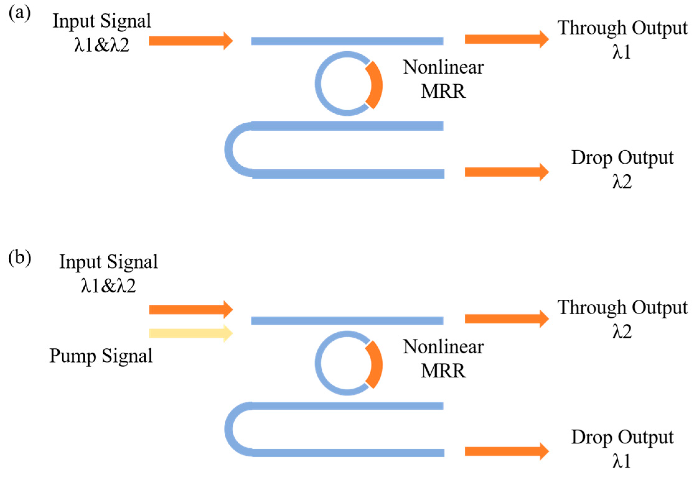
2.1. Nonlinear MRR
2.2. Optical Standard Logic Unit (OSLU)
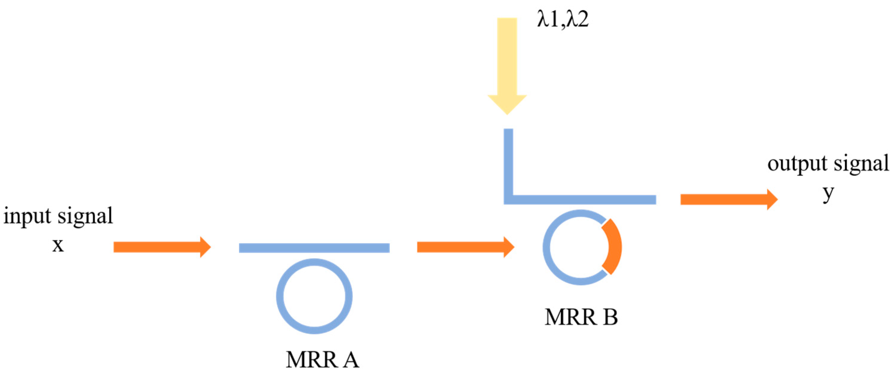
2.2.1. The OSLU for IS&NOT
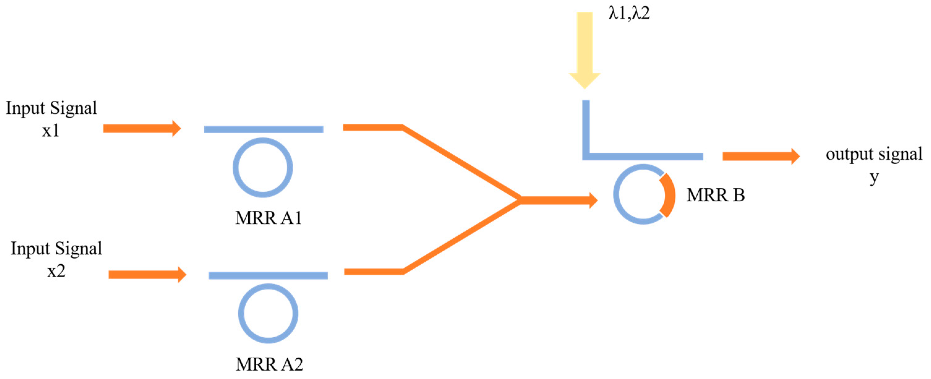
2.2.2. The Function of AND
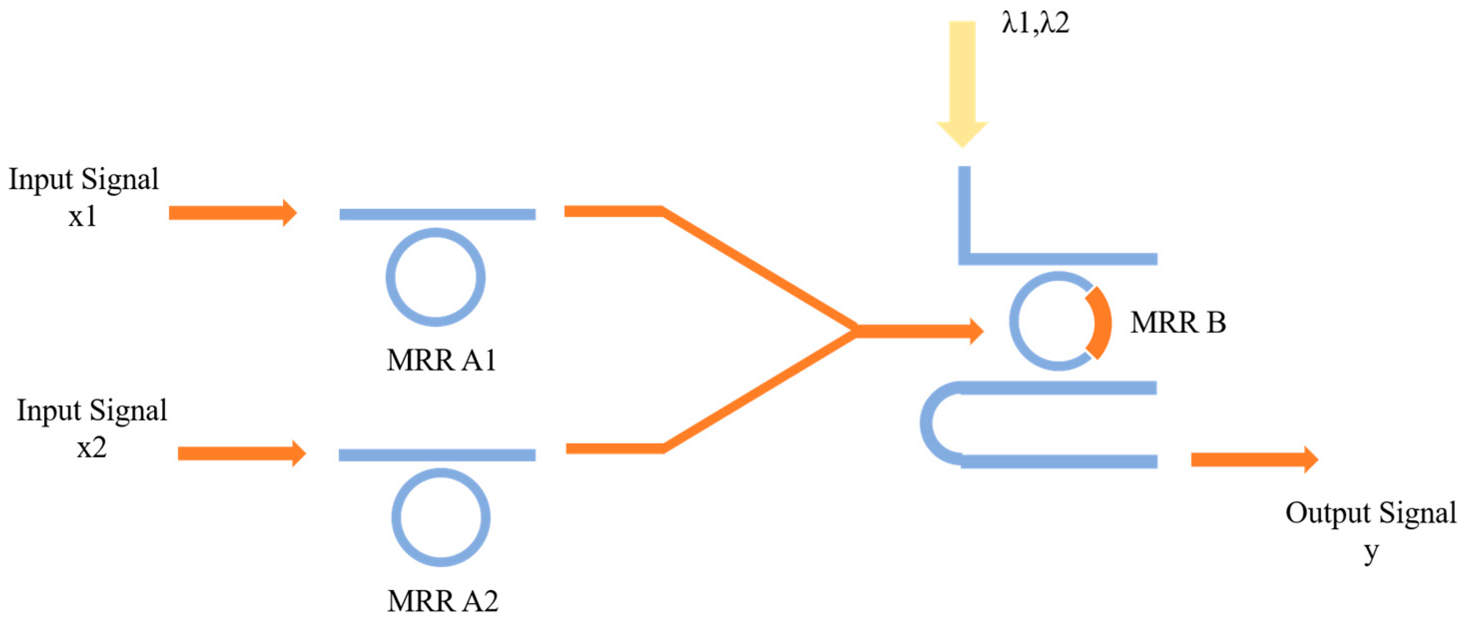
2.2.3. The Function of OR
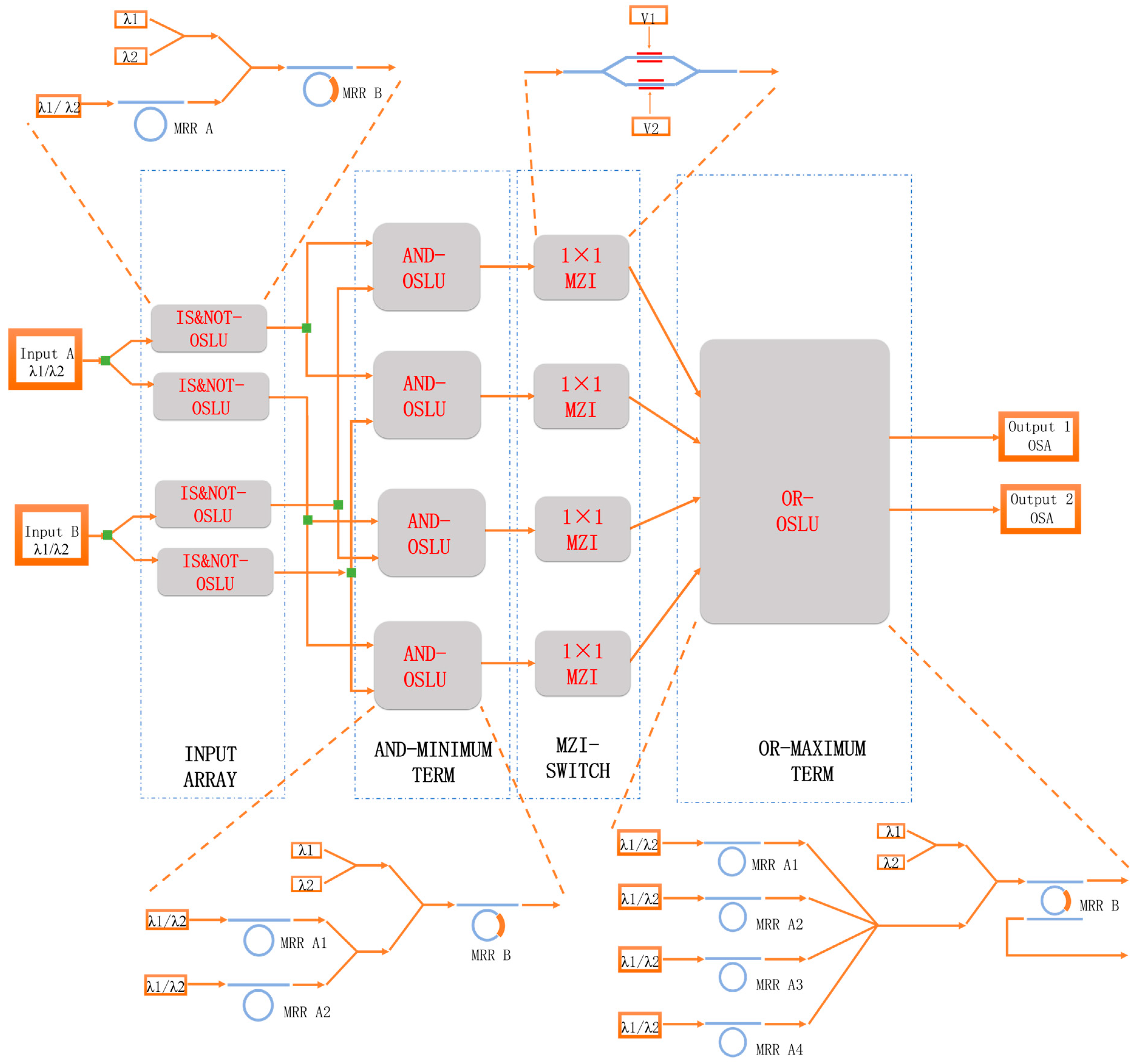
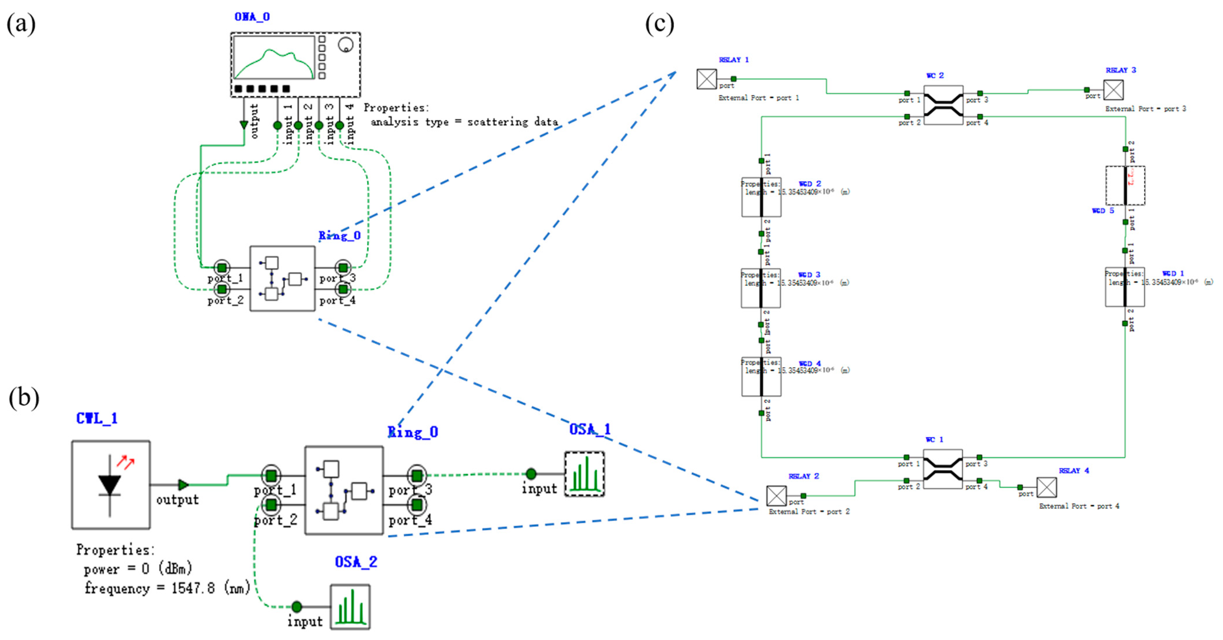
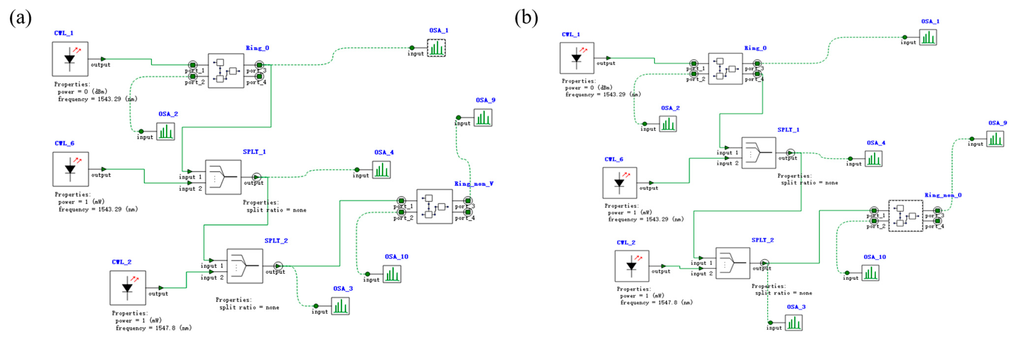
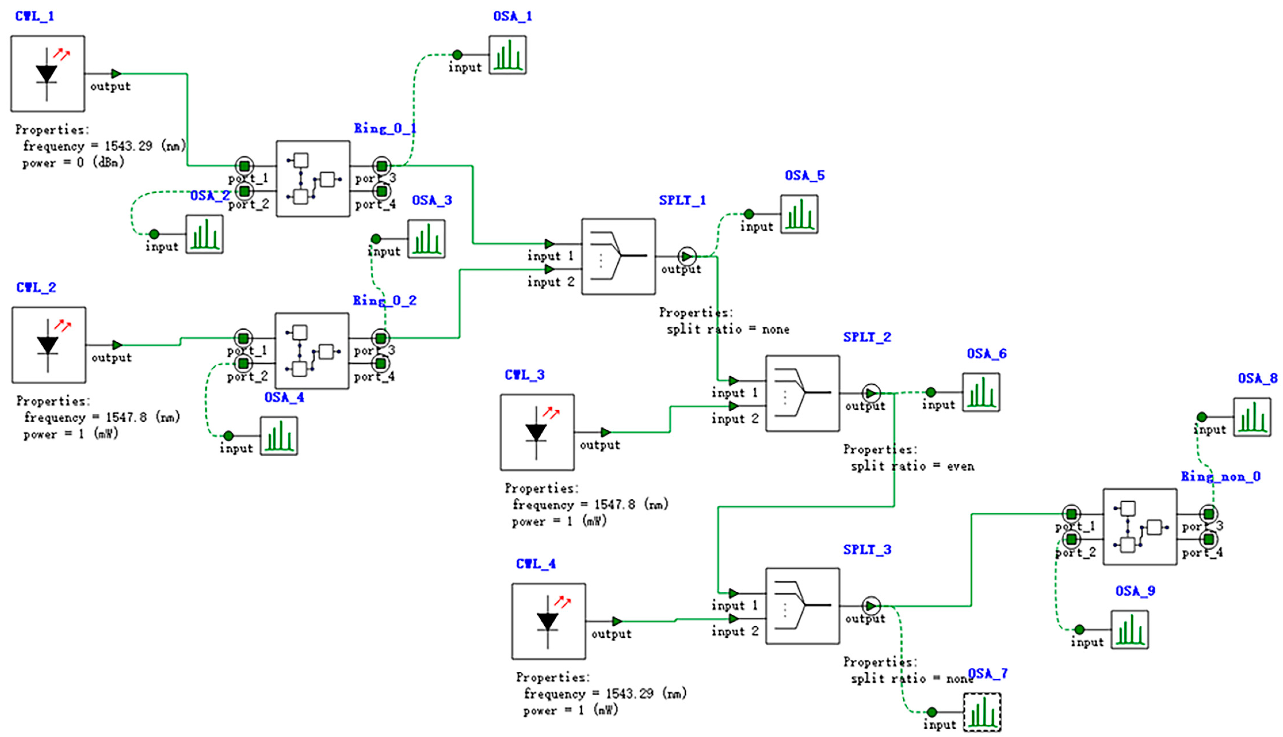
2.3. Programmable Photonic Logic Array (PPLA)
3. Simulation Results
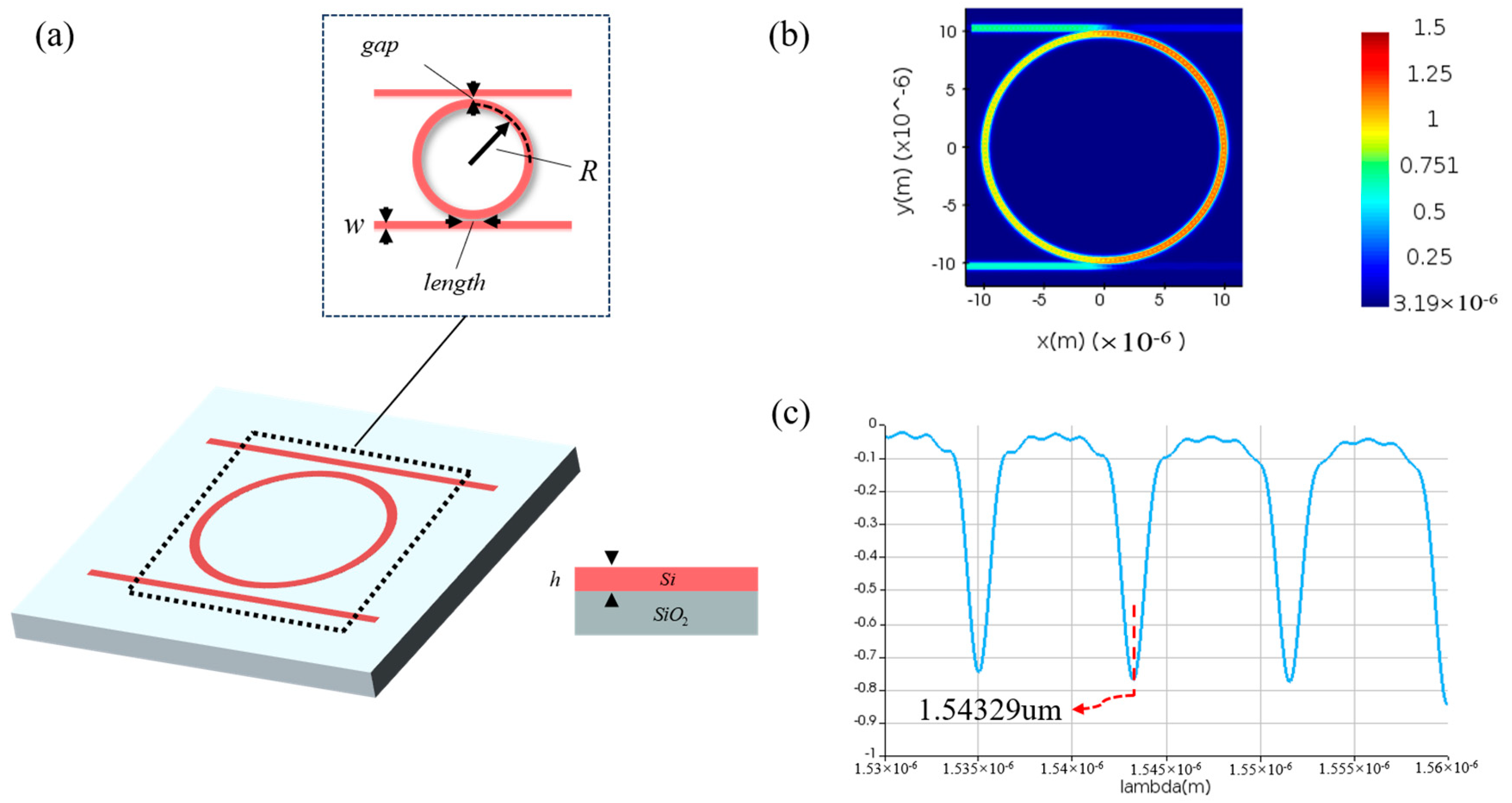
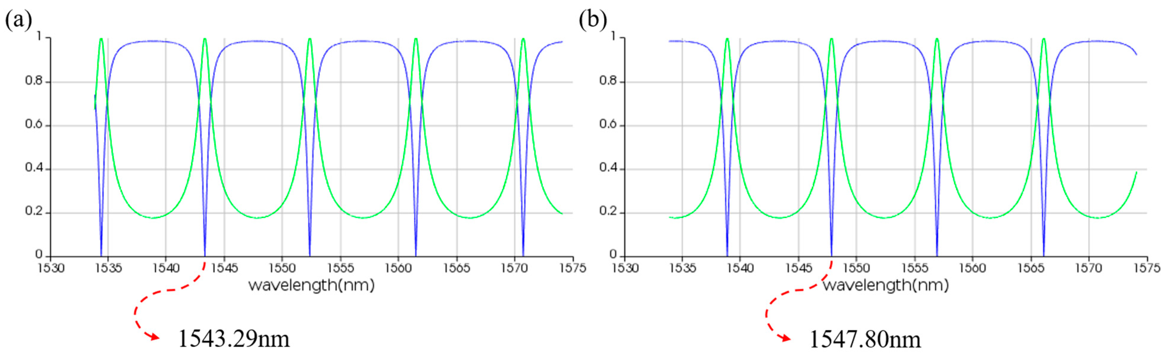
3.1. Micro-Ring Resonator (MRR)
3.1.1. Linear MRR
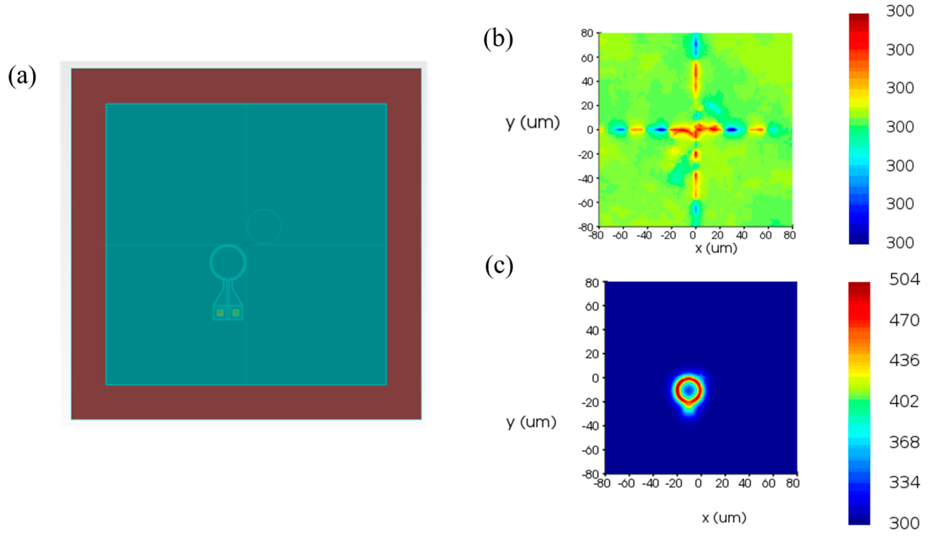
3.1.2. Nonlinear MRR
3.2. OSLU
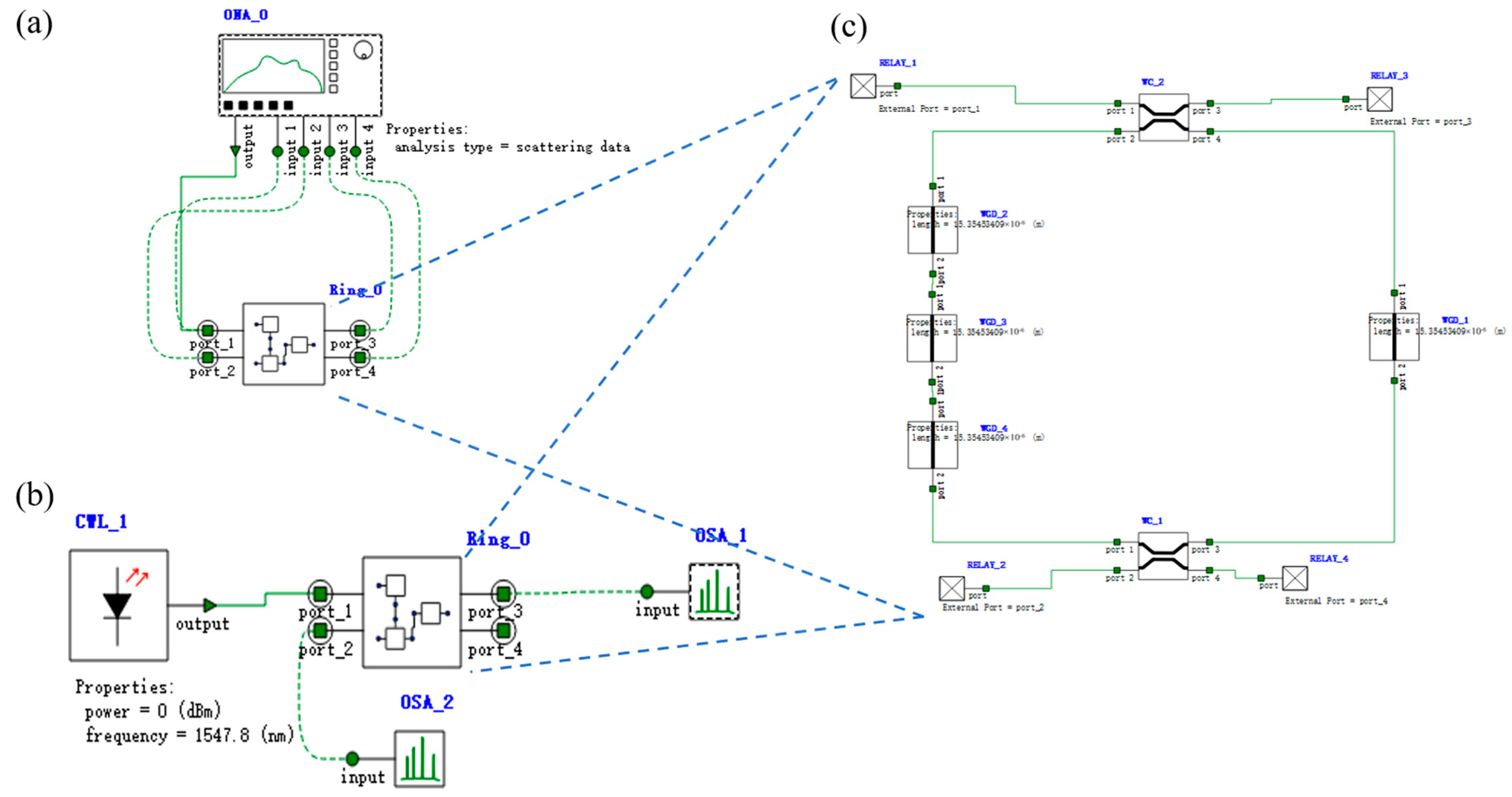
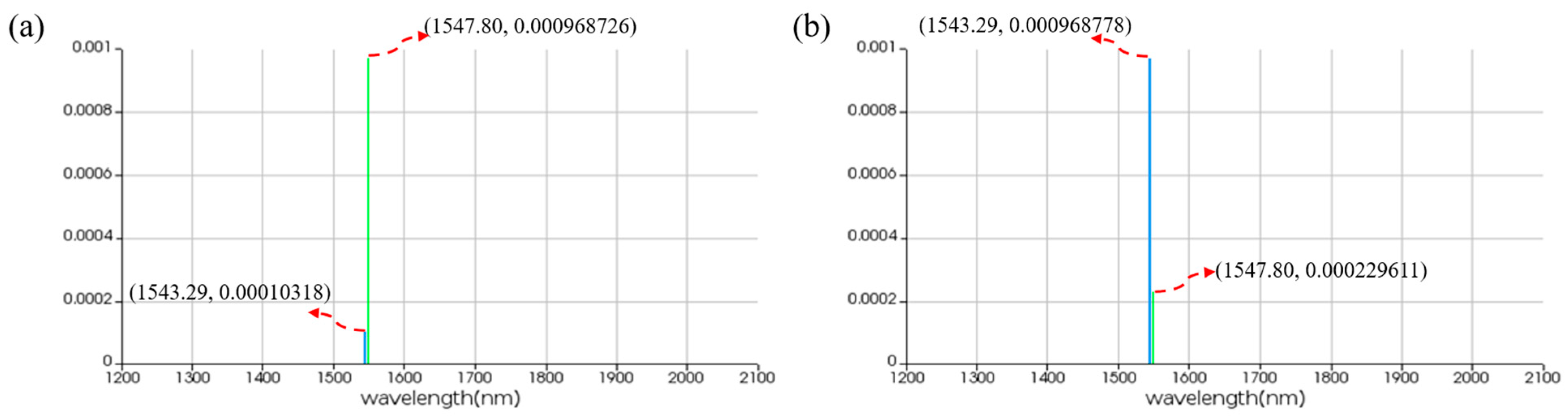
3.2.1. The OSLU of IS&NOT
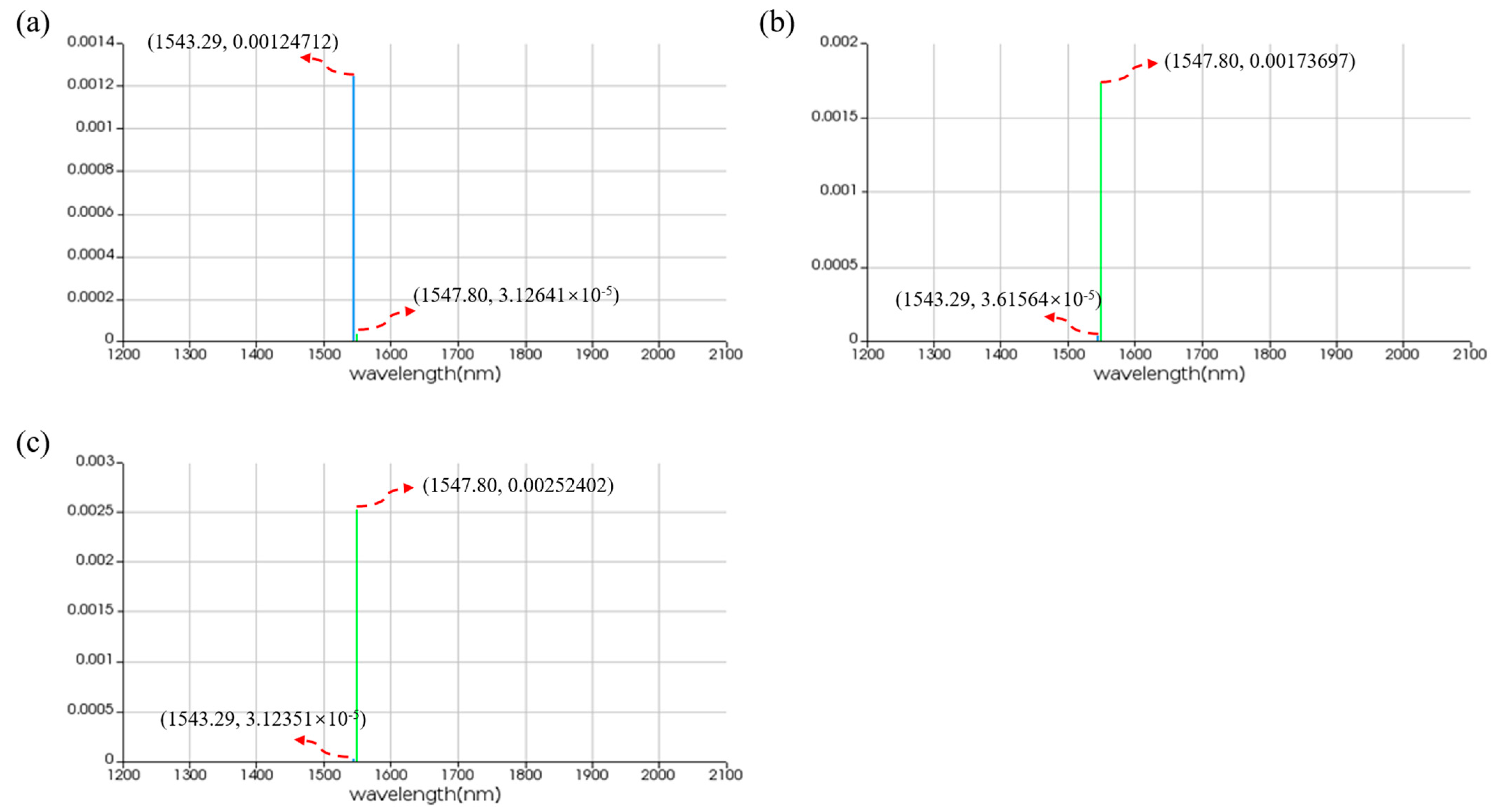
3.2.2. The OSLU of AND
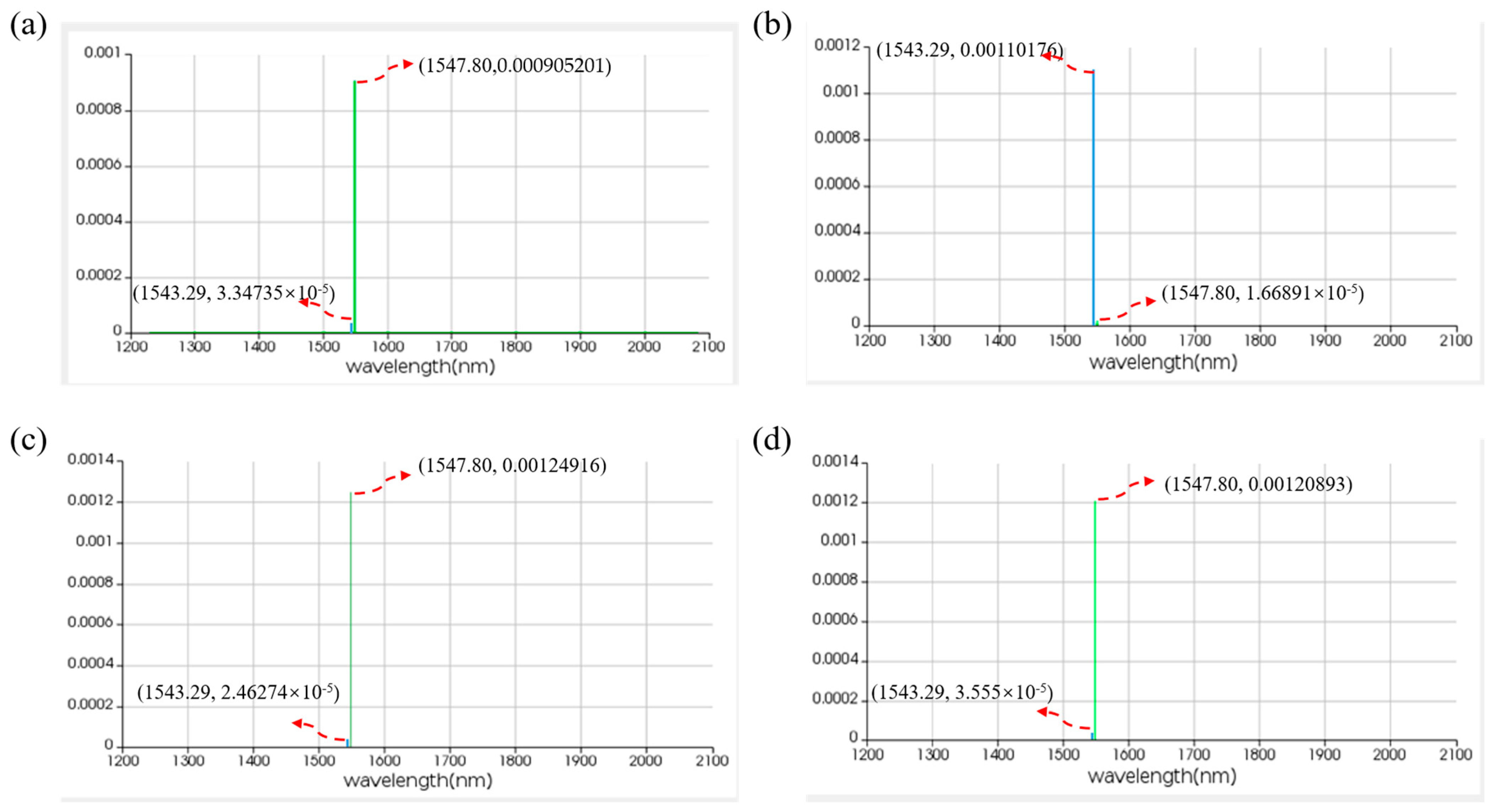
3.2.3. The OSLU of OR
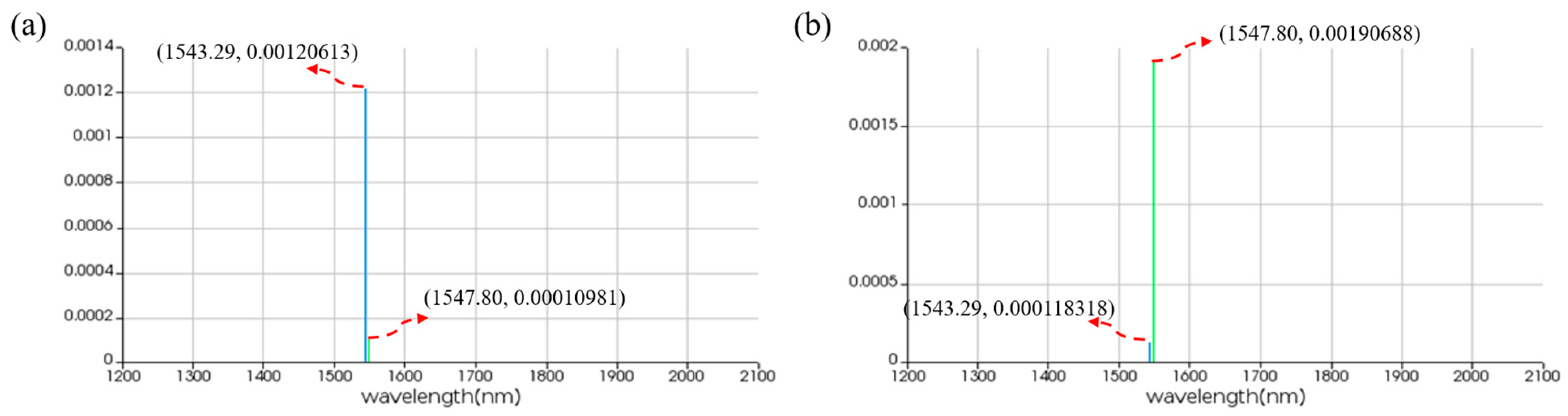
3.3. Simulation Results of the Two-Input PPLA
4. Conclusions
Author Contributions
Funding
Data Availability Statement
Conflicts of Interest
References
- Wang, Y.; Yang, H.; Dong, W.; Lei, L.; Xu, J.; Zhang, X.; Xu, P. Highly Nonlinear Organic-Silicon Slot Waveguide for Ultrafast Multimode All-Optical Logic Operations. IEEE Photonics J. 2020, 12, 1–12. [Google Scholar] [CrossRef]
- Dong, W.; Lei, L.; Chen, L.; Yu, Y.; Zhang, X. All-Optical 2 × 2-Bit Multiplier at 40 Gb/s Based on Canonical Logic Units-based Programmable Logic Array (CLUs-PLA). J. Light. Technol. 2020, 38, 5586–5594. [Google Scholar] [CrossRef]
- Dong, W.; Hou, J.; Zhang, X. Investigation on Expanding the Computing Capacity of Optical Programmable Logic Array Based on Canonical Logic Units. J. Light. Technol. 2018, 36, 3949–3958. [Google Scholar] [CrossRef]
- Giamougiannis, G.; Tsakyridis, A.; Moralis-Pegios, M.; Pappas, C.; Kirtas, M.; Passalis, N.; Lazovsky, D.; Tefas, A.; Pleros, N. Analog nanophotonic computing going practical: Silicon photonic deep learning engines for tiled optical matrix multiplication with dynamic precision. Nanophotonics 2023, 12, 963–973. [Google Scholar] [CrossRef]
- Mehrabian, A.; Miscuglio, M.; Alkabani, Y.; Sorger, V.; El-Ghazawi, T. A Winograd-based integrated photonics accelerator for convolutional neural networks. IEEE J. Sel. Top. Quantum Electron. 2020, 26, 6100312. [Google Scholar] [CrossRef]
- Gu, J.; Feng, C.; Zhao, Z.; Ying, Z.; Liu, M.; Chen, R.; Pan, D. SqueezeLight: Towards scalable optical neural networks with multi-operand ring resonators. In Proceedings of the Design, Automation & Test in Europe Conference & Exhibition (DATE), Grenoble, France, 1–5 February 2021; pp. 238–243. [Google Scholar] [CrossRef]
- Liu, J.; Wu, Q.; Sui, X.; Chen, Q.; Gu, G.; Wang, L.; Li, S. Research progress in optical neural networks: Theory, applications and developments. PhotoniX 2021, 2, 1–39. [Google Scholar] [CrossRef]
- Zhang, L.; Ji, R.; Jia, L.; Yang, L.; Zhou, P.; Tian, Y.; Chen, P.; Lu, Y.; Jiang, Z.; Liu, Y.; et al. Demonstration of directed XOR/XNOR logic gates using two cascaded microring resonators. Opt. Lett. 2010, 35, 1620–1622. [Google Scholar] [CrossRef]
- Tian, Y.; Zhang, L.; Ji, R.; Yang, L.; Zhou, P.; Chen, H.; Ding, J.; Zhu, W.; Lu, Y.; Jia, L.; et al. Proof of concept of directed OR/NOR and AND/NAND logic circuit consisting of two parallel microring resonators. Opt. Lett. 2011, 36, 1650–1652. [Google Scholar] [CrossRef] [PubMed]
- Tian, Y.; Yang, L.; Zhang, L.; Ji, R.; Ding, J.; Zhou, P.; Zhu, W.; Lu, Y. Directed optical half-adder based on two cascaded microring resonators. IEEE Photon. Technol. Lett. 2012, 24, 643–645. [Google Scholar] [CrossRef]
- Wu, X.; Deng, L.; Meng, Y.; Yang, J.; Tian, Y. Demonstration of a silicon photonic circuit for half-add operations using cascaded microring resonators. IEEE Photon. J. 2016, 9, 2700209. [Google Scholar] [CrossRef]
- Liu, Z.; Zhao, Y.; Xiao, H.; Deng, L.; Meng, Y.; Guo, X.; Liu, G.; Tian, Y.; Yang, J. Demonstration of an optical directed half-subtracter using integrated silicon photonic circuits. Appl. Opt. 2018, 57, 2564–2569. [Google Scholar] [CrossRef] [PubMed]
- Tian, Y.; Zhang, L.; Ji, R.; Yang, L.; Xu, Q. Demonstration of a directed optical encoder using microring-resonator-based optical switches. Opt. Lett. 2011, 36, 3795–3797. [Google Scholar] [CrossRef] [PubMed]
- Xiao, H.; Li, D.; Liu, Z.; Han, H.; Chen, W.; Zhao, T.; Tian, Y.; Yang, J. Experimental realization of a CMOS-compatible optical directed priority encoder using cascaded micro-ring resonators. Nanophotonics 2018, 7, 727–733. [Google Scholar] [CrossRef]
- Chen, Q.; Zhang, F.; Zhang, L.; Tian, Y.; Zhou, P.; Ding, J.; Yang, L. 1 Gbps directed optical decoder based on two cascaded microring resonators. Opt. Lett. 2014, 39, 4255–4258. [Google Scholar] [CrossRef] [PubMed]
- Yang, L.; Guo, C.; Zhu, W.; Zhang, L.; Sun, C. Demonstration of a directed optical comparator based on two cascaded microring resonators. IEEE Photon. Technol. Lett. 2015, 27, 809–812. [Google Scholar] [CrossRef]
- Tian, Y.; Xiao, H.; Wu, X.; Liu, Z.; Meng, Y.; Deng, L.; Guo, X.; Liu, G.; Yang, J. Experimental realization of an optical digital comparator using silicon microring resonators. Nanophotonics 2018, 7, 669–675. [Google Scholar] [CrossRef]
- Law, F.K.; Uddin, M.R.; Hashim, H.; Won, Y.H. Demonstration of photonic micro-ring resonator based digital bit magnitude comparator. Opt. Quant. Electron. 2019, 51, 1–13. [Google Scholar] [CrossRef]
- Liu, Z.; Wu, X.; Xiao, H.; Han, X.; Chen, W.; Liao, M.; Zhao, T.; Jia, H.; Yang, J.; Tian, Y. On-chip optical parity checker using silicon photonic integrated circuits. Nanophotonics 2018, 7, 1939–1948. [Google Scholar] [CrossRef]
- Tian, Y.; Liu, Z.; Ying, T.; Xiao, H.; Meng, Y.; Deng, L.; Zhao, Y.; Guo, A.; Liao, M.; Liu, G.; et al. Experimental demonstration of an optical Feynman gate for reversible logic operation using silicon micro-ring resonators. Nanophotonics 2018, 7, 333–337. [Google Scholar] [CrossRef]
- Chen, F.; Zhou, S.; Xia, Y.; Yu, X.; Liu, J.; Li, F.; Siu, X. Ultra-compact optical full-adder based on directed logic and microring resonators. Appl. Opt. 2024, 63, 147–153. [Google Scholar] [CrossRef] [PubMed]
- Xia, Y.; Zhou, S.; Chen, F.; Yu, X.; Liu, J.; Li, F.; Siu, X. A multifunctional optical computing system based on directed logic and micro-ring resonator. Opt. Laser Technol. 2024, 175, 110696. [Google Scholar] [CrossRef]
- Xu, Q.; Lipson, M. All-optical logic based on silicon microring resonators. Opt. Express 2007, 15, 924–929. [Google Scholar] [CrossRef] [PubMed]
- Dong, W.; Hou, J.; Zhang, X. All-optical reconfigurable multicast canonical logic units based on four-wave mixing. Electron. Lett. 2017, 53, 1321–1323. [Google Scholar] [CrossRef]
- Dong, W.; Huang, Z.; Hou, J.; Santos, R. Integrated all-optical programmable logic array based on semiconductor optical amplifiers. Opt. Lett. 2018, 43, 2150–2153. [Google Scholar] [CrossRef]
- Zhang, W.; Dong, W. Integrated All-Optical Programmable Logic Array Based on Cross Gain Modulation. Hans. J. Wirel. Commun. 2019, 9, 14. [Google Scholar] [CrossRef]
- Gao, X.; Gu, W.; Dong, W.; Zhou, H.; Lei, L.; Chen, L.; Yu, Y.; Dong, J.; Zhang, X. Seven-channel all-optical reconfigurable canonical logic units multicasting at 40 Gb/s based on a nonlinearity-enhanced silicon waveguide. Opt. Express 2022, 30, 32650. [Google Scholar] [CrossRef] [PubMed]
- Hou, J.; Chen, L.; Dong, W.; Zhang, X. 40 Gb/s reconfigurable optical logic gates based on FWM in silicon waveguide. Opt. Express 2016, 24, 2701. [Google Scholar] [CrossRef]
- Wang, J.; Sun, J.; Sun, Q.; Zhang, X.; Huang, D. Simple realization of all-optical high-speed (40, 80 and 160 Gb s−1) XOR and OR logic gates using LiNbO3 waveguides. J. Opt. A Pure Appl. Opt. 2007, 9, 811. [Google Scholar] [CrossRef]
- Tong, Y.; Li, D.; Li, J. All-Optical OR Gate with Single Wavelength Based on PPLN Waveguides. Laser Optoelectron. Prog. 2018, 55, 092301. [Google Scholar] [CrossRef]
- Sharma, N.; Singh, S. Reconfigurable all-optical logic device based on cross-phase modulation across highly non-linear fiber. Opt. Fiber Technol. 2023, 81, 103567. [Google Scholar] [CrossRef]
- Singh, K.; Kaur, G.; Singh, M.L. Enhanced performance of all-optical half-subtracter based on cross-gain modulation (XGM) in semiconductor optical amplifier (SOA) by accelerating its gain recovery dynamics. Photonic Netw. Commun. 2017, 34, 111–130. [Google Scholar] [CrossRef]
- Tian, Y.; Zhao, G.; Liu, Z.; Guo, A.; Xiao, H.; Wu, X.; Meng, Y.; Deng, L.; Guo, X.; Liu, G.; et al. Reconfgurable electro-optic logic circuits using microring resonator-based optical switch array. IEEE Photon. J. 2016, 8, 7801908. [Google Scholar] [CrossRef]
- Zhang, X.; Wang, Y.; Sun, J.; Liu, D.; Huang, D. All-optical AND gate at 10 Gbit/s based on cascaded single-port-coupled SOAs. Opt. Express 2004, 12, 361–366. [Google Scholar] [CrossRef]
- Dong, J.; Zhang, X.; Fu, S.; Xu, J.; Shum, P.; Huang, D. Ultrafast All-Optical Signal Processing Based on Single Semiconductor Optical Amplifier and Optical Filtering. IEEE J. Sel. Top. Quantum Electron. 2008, 14, 770–778. [Google Scholar] [CrossRef]
- Xu, J.; Zhang, X.; Zhang, Y.; Dong, J.; Liu, D.; Huang, D. Reconfigurable All-Optical Logic Gates for Multi-Input Differential Phase-Shift Keying Signals: Design and Experiments. J. Light. Technol. 2009, 27, 5268–5275. [Google Scholar] [CrossRef]
- Zhang, Y.; Lei, L.; Dong, J.; Zhang, X. Simultaneous all-optical digital comparator and dual-directional half-subtractor for two-input 40Gbit/s DPSK signals employing SOAs. Opt. Commun. 2012, 285, 407–411. [Google Scholar] [CrossRef]


| VARIABLE | RESULT | ||||||||
|---|---|---|---|---|---|---|---|---|---|
| A | B | Function | m1 + m2 | m1 + m3 | m1 + m4 | m2 + m3 | m2 + m4 | m3 + m4 | |
| Characterization | |||||||||
| 0 | 0 | Logic | 1 | 1 | 1 | 0 | 0 | 0 | |
| Wavelength/nm | 1547.80 | 1547.80 | 1547.80 | 1543.29 | 1543.29 | 1543.29 | |||
| Power/mW | 0.73873 | 0.73873 | 0.874803 | 1.02054 | 0.99038 | 0.99038 | |||
| 0 | 1 | Logic | 1 | 0 | 0 | 1 | 1 | 0 | |
| Wavelength/nm | 1547.80 | 1543.29 | 1543.29 | 1547.80 | 1547.80 | 1543.29 | |||
| Power/mW | 0.761208 | 1.00962 | 1.02431 | 1.26058 | 0.743831 | 0.994258 | |||
| 1 | 0 | Logic | 0 | 1 | 0 | 1 | 0 | 1 | |
| Wavelength/nm | 1543.29 | 1547.80 | 1543.29 | 1547.80 | 1543.29 | 1547.80 | |||
| Power/mW | 1.00917 | 1.03859 | 1.02561 | 1.26058 | 0.969297 | 0.978895 | |||
| 1 | 1 | Logic | 0 | 0 | 1 | 0 | 1 | 1 | |
| Wavelength/nm | 1543.29 | 1543.29 | 1547.80 | 1543.29 | 1547.80 | 1547.80 | |||
| Power/mW | 1.0151 | 1.0151 | 1.46462 | 1.03151 | 1.13397 | 1.13397 | |||
| VARIABLE | RESULT | ||||||
|---|---|---|---|---|---|---|---|
| A | B | Function | m1 + m2 + m3 | m1 + m2 + m4 | m1 + m3 + m4 | m2 + m3 + m4 | |
| Characterization | |||||||
| 0 | 0 | Logic | 1 | 1 | 1 | 0 | |
| Wavelength/nm | 1547.80 | 1547.80 | 1547.80 | 1543.29 | |||
| Power/mW | 0.773708 | 0.905201 | 0.905201 | 1.08678 | |||
| 0 | 1 | Logic | 1 | 1 | 0 | 1 | |
| Wavelength/nm | 1547.80 | 1547.80 | 1543.29 | 1547.80 | |||
| Power/mW | 0.936886 | 1.05891 | 1.10176 | 0.917892 | |||
| 1 | 0 | Logic | 1 | 0 | 1 | 1 | |
| Wavelength/nm | 1547.80 | 1543.29 | 1547.80 | 1547.80 | |||
| Power/mW | 0.884492 | 1.04617 | 1.24916 | 1.26968 | |||
| 1 | 1 | Logic | 0 | 1 | 1 | 1 | |
| Wavelength/nm | 1543.29 | 1547.80 | 1547.80 | 1547.80 | |||
| Power/mW | 1.1199 | 1.20893 | 1.20893 | 0.948801 | |||
| VARIABLE | RESULT | |||
|---|---|---|---|---|
| A | B | Function | m1 + m2 + m3 + m4 | |
| Characterization | 1 | |||
| 0 | 0 | Logic | 1 | |
| Wavelength/nm | 1547.80 | |||
| Power/mW | 0.949655 | |||
| 0 | 1 | Logic | 1 | |
| Wavelength/nm | 1547.80 | |||
| Power/mW | 0.973804 | |||
| 1 | 0 | Logic | 1 | |
| Wavelength/nm | 1547.80 | |||
| Power/mW | 1.36479 | |||
| 1 | 1 | Logic | 1 | |
| Wavelength/nm | 1547.80 | |||
| Power/mW | 0.800419 | |||
Disclaimer/Publisher’s Note: The statements, opinions and data contained in all publications are solely those of the individual author(s) and contributor(s) and not of MDPI and/or the editor(s). MDPI and/or the editor(s) disclaim responsibility for any injury to people or property resulting from any ideas, methods, instructions or products referred to in the content. |
© 2025 by the authors. Licensee MDPI, Basel, Switzerland. This article is an open access article distributed under the terms and conditions of the Creative Commons Attribution (CC BY) license (https://creativecommons.org/licenses/by/4.0/).
Share and Cite
Liu, J.; Zhou, S.; Sui, X. Programmable Photonic Logic Array Based on Micro-Ring Resonators and All-Optical Modulation. Micromachines 2025, 16, 238. https://doi.org/10.3390/mi16020238
Liu J, Zhou S, Sui X. Programmable Photonic Logic Array Based on Micro-Ring Resonators and All-Optical Modulation. Micromachines. 2025; 16(2):238. https://doi.org/10.3390/mi16020238
Chicago/Turabian StyleLiu, Jia, Shenghang Zhou, and Xiubao Sui. 2025. "Programmable Photonic Logic Array Based on Micro-Ring Resonators and All-Optical Modulation" Micromachines 16, no. 2: 238. https://doi.org/10.3390/mi16020238
APA StyleLiu, J., Zhou, S., & Sui, X. (2025). Programmable Photonic Logic Array Based on Micro-Ring Resonators and All-Optical Modulation. Micromachines, 16(2), 238. https://doi.org/10.3390/mi16020238