Performance Analysis and Optimization of an InGaAs/GaAsSb Heterojunction Dopingless Tunnel FET with a Heterogate Dielectric
Abstract
1. Introduction
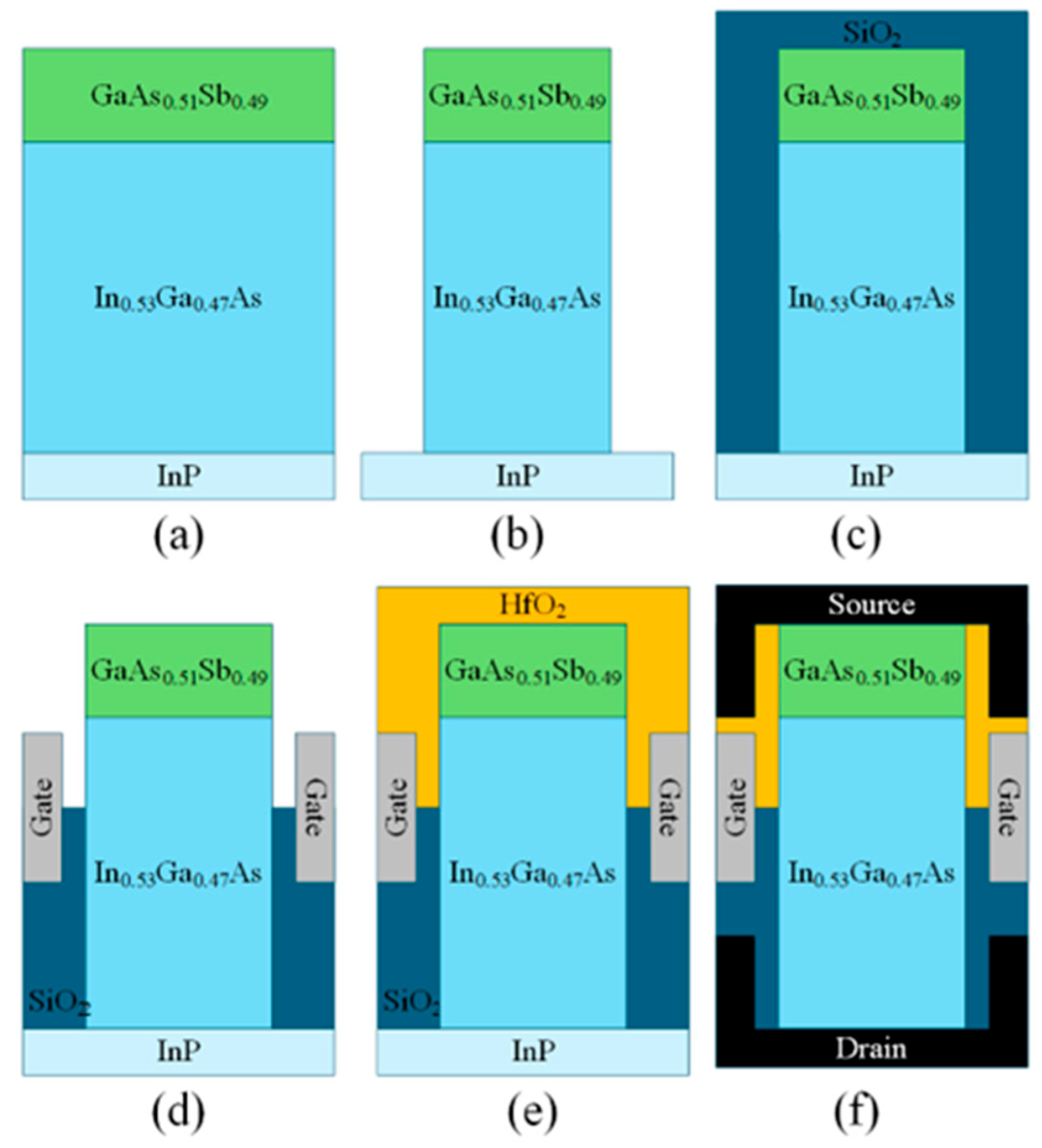
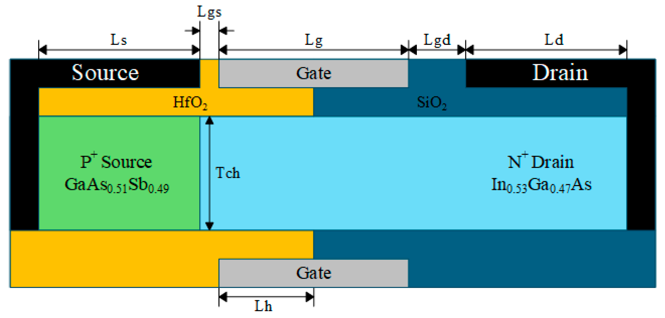
2. Device Structure and Model
3. Results and Discussion
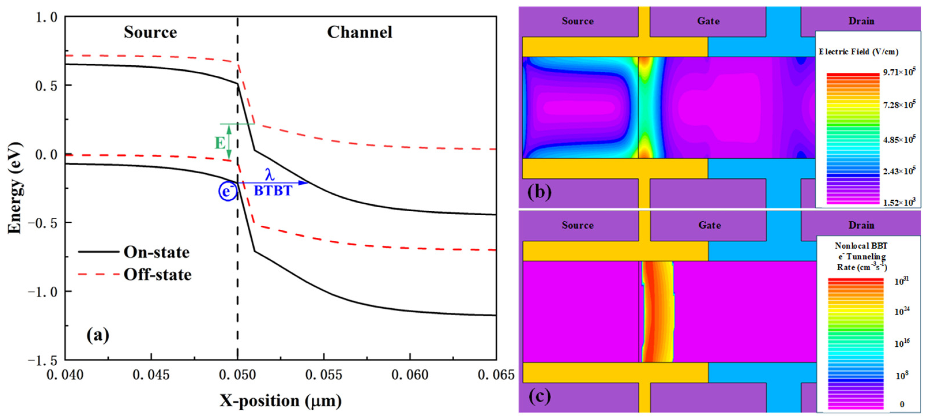
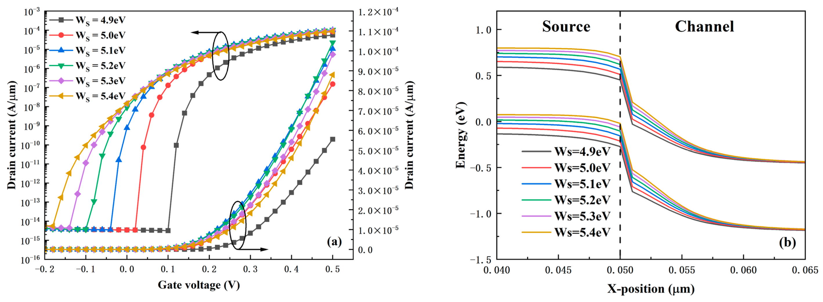
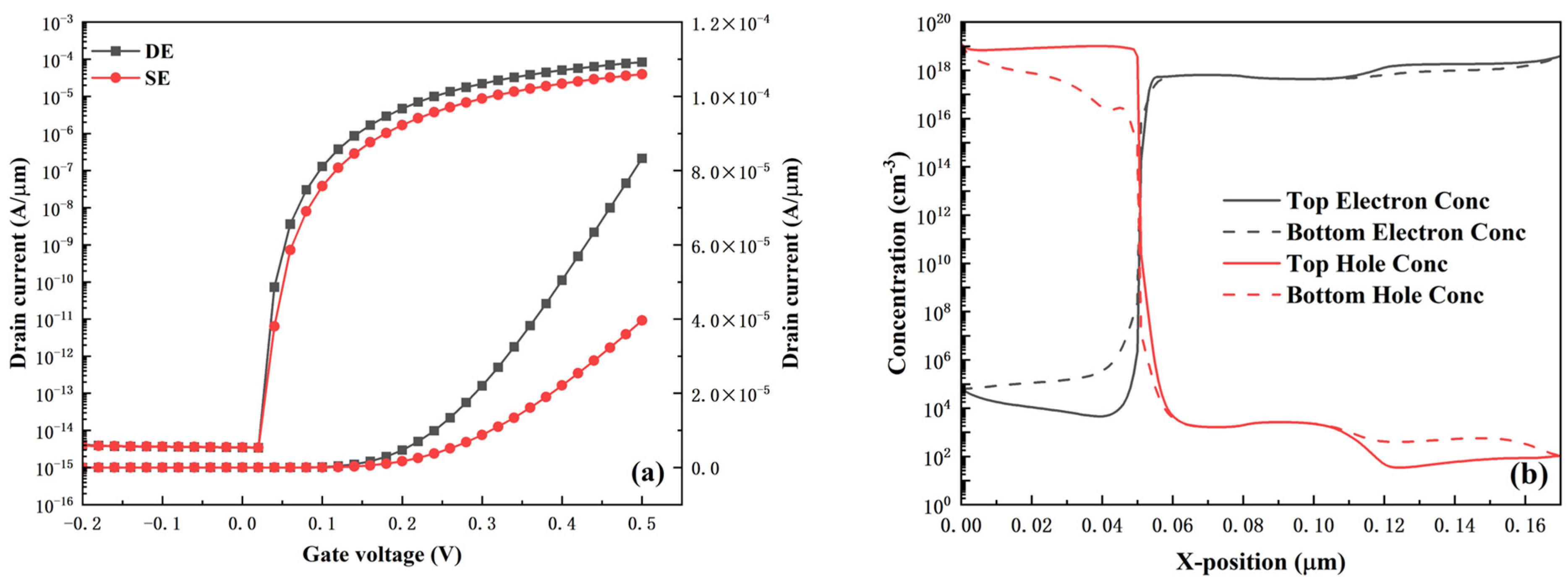
3.1. Operating Mechanism of the HDL-TFET
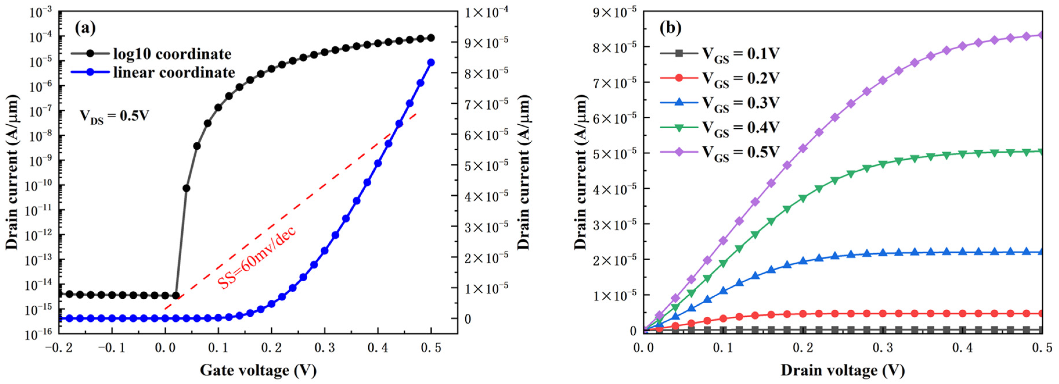
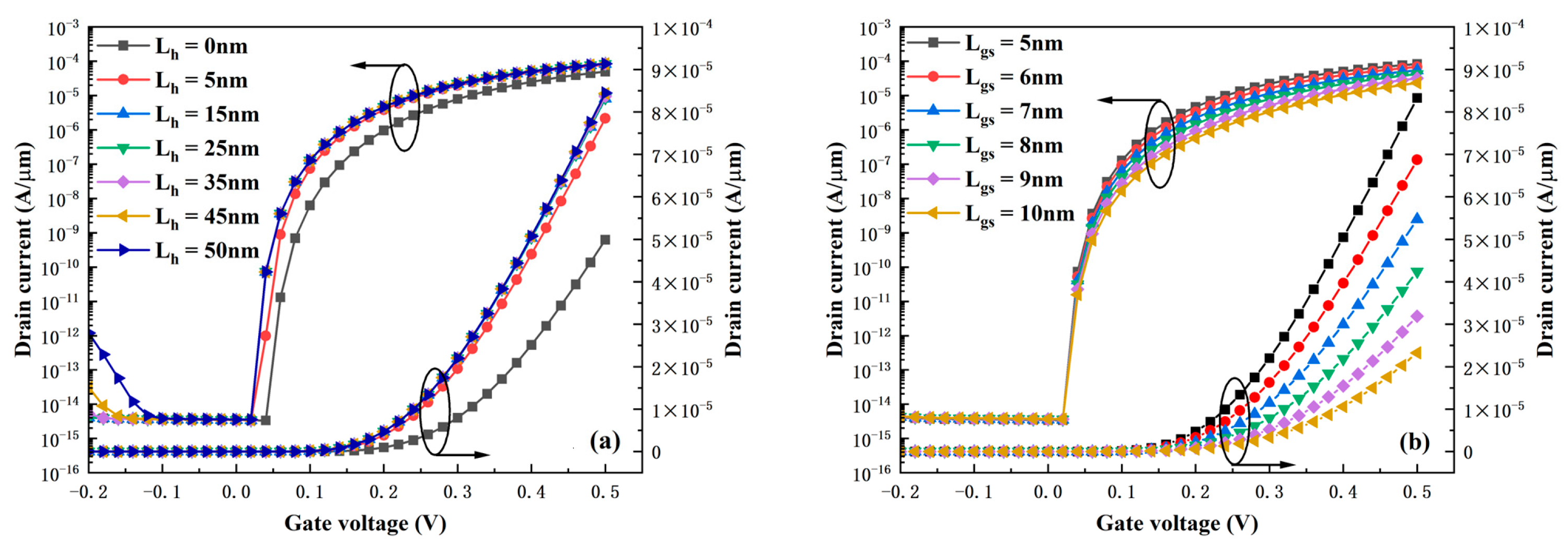
3.2. Effect of Device Parameters on Performance
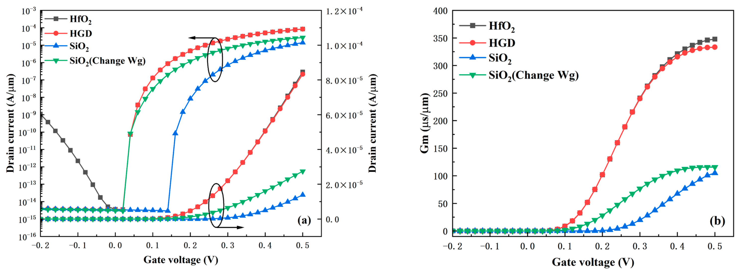
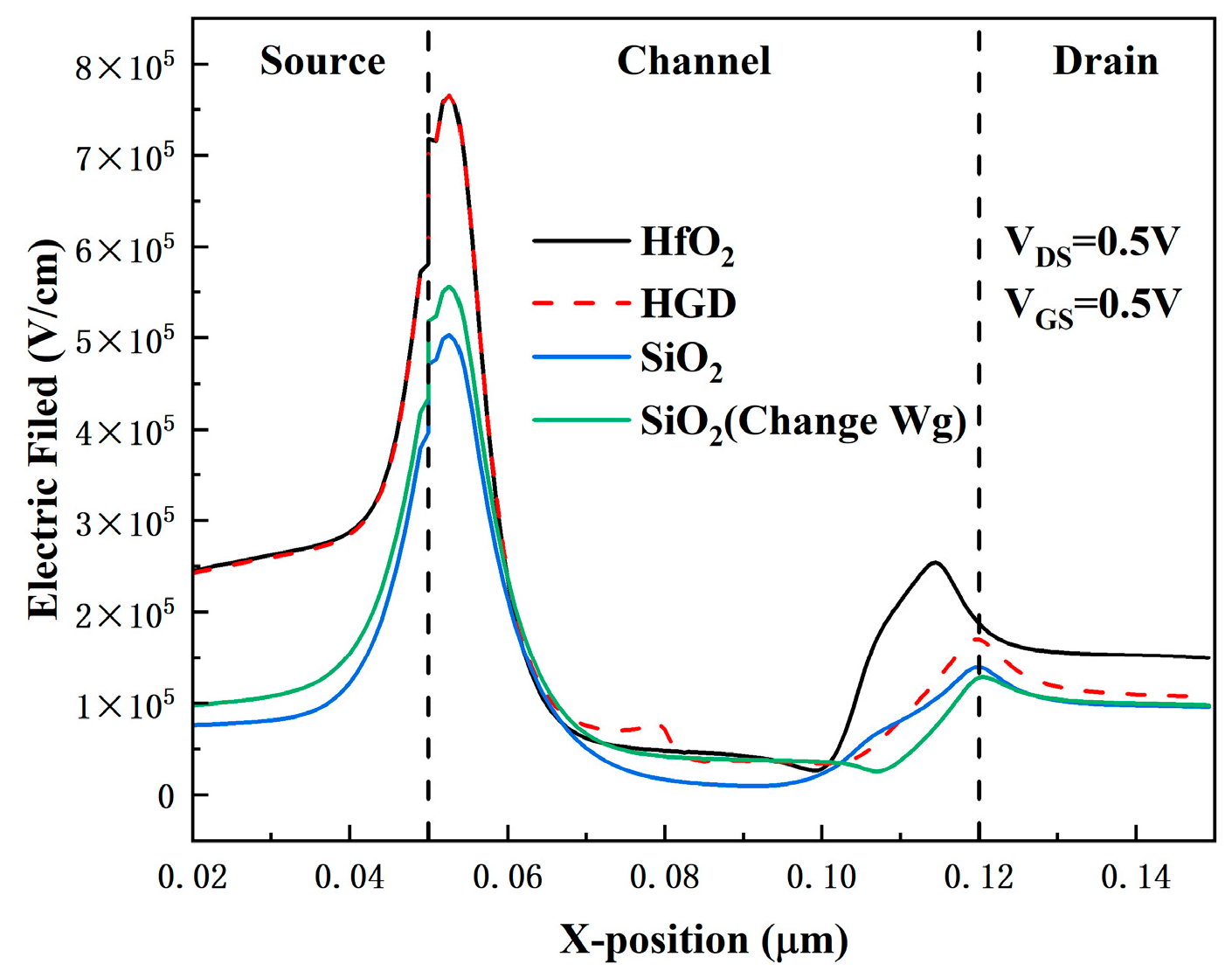
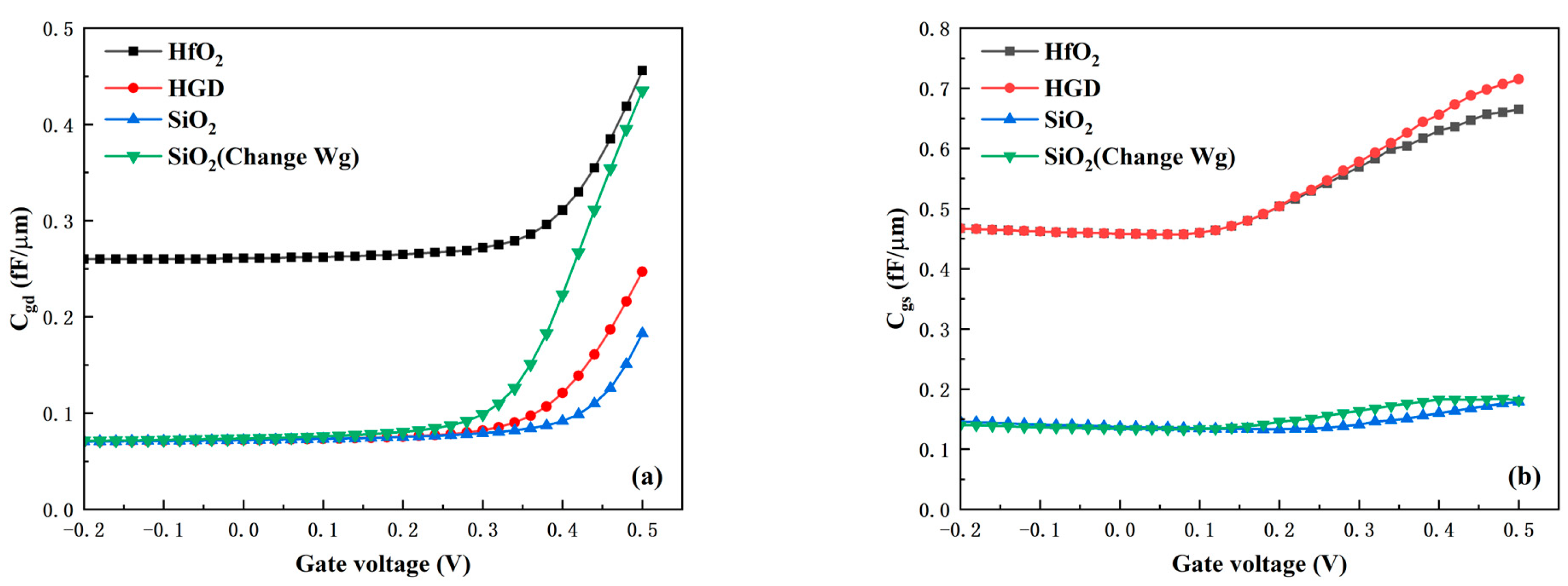
3.3. Heterogate Dielectric Engineering
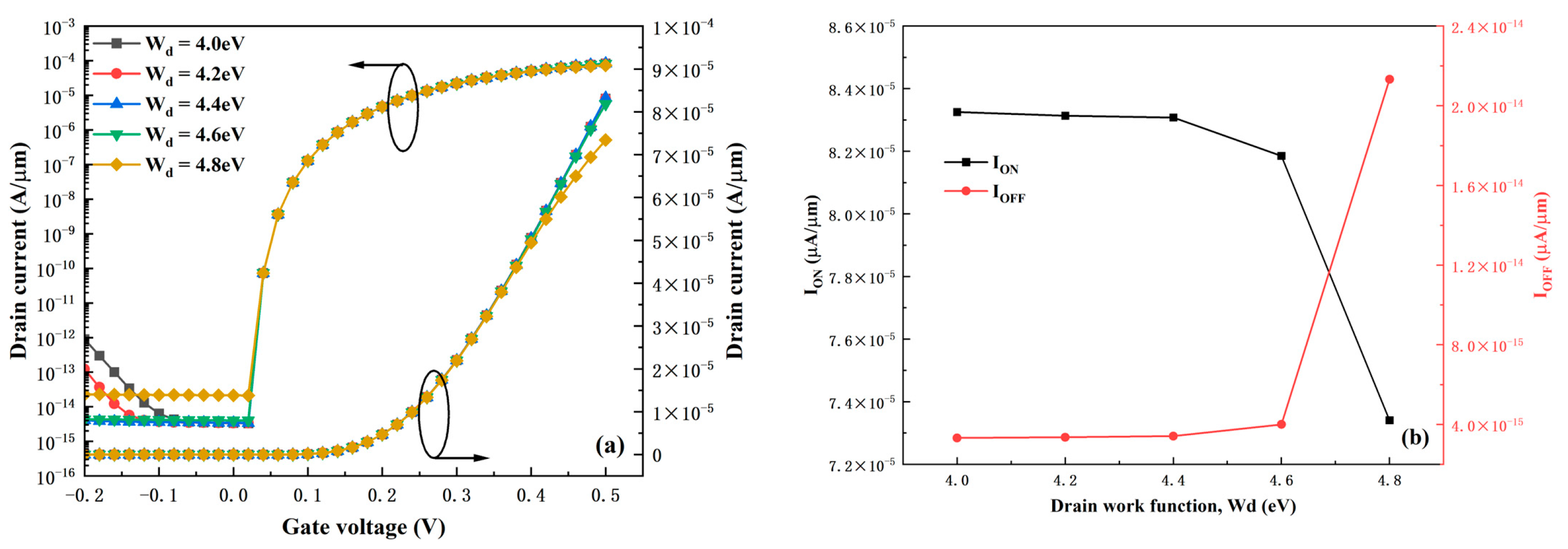
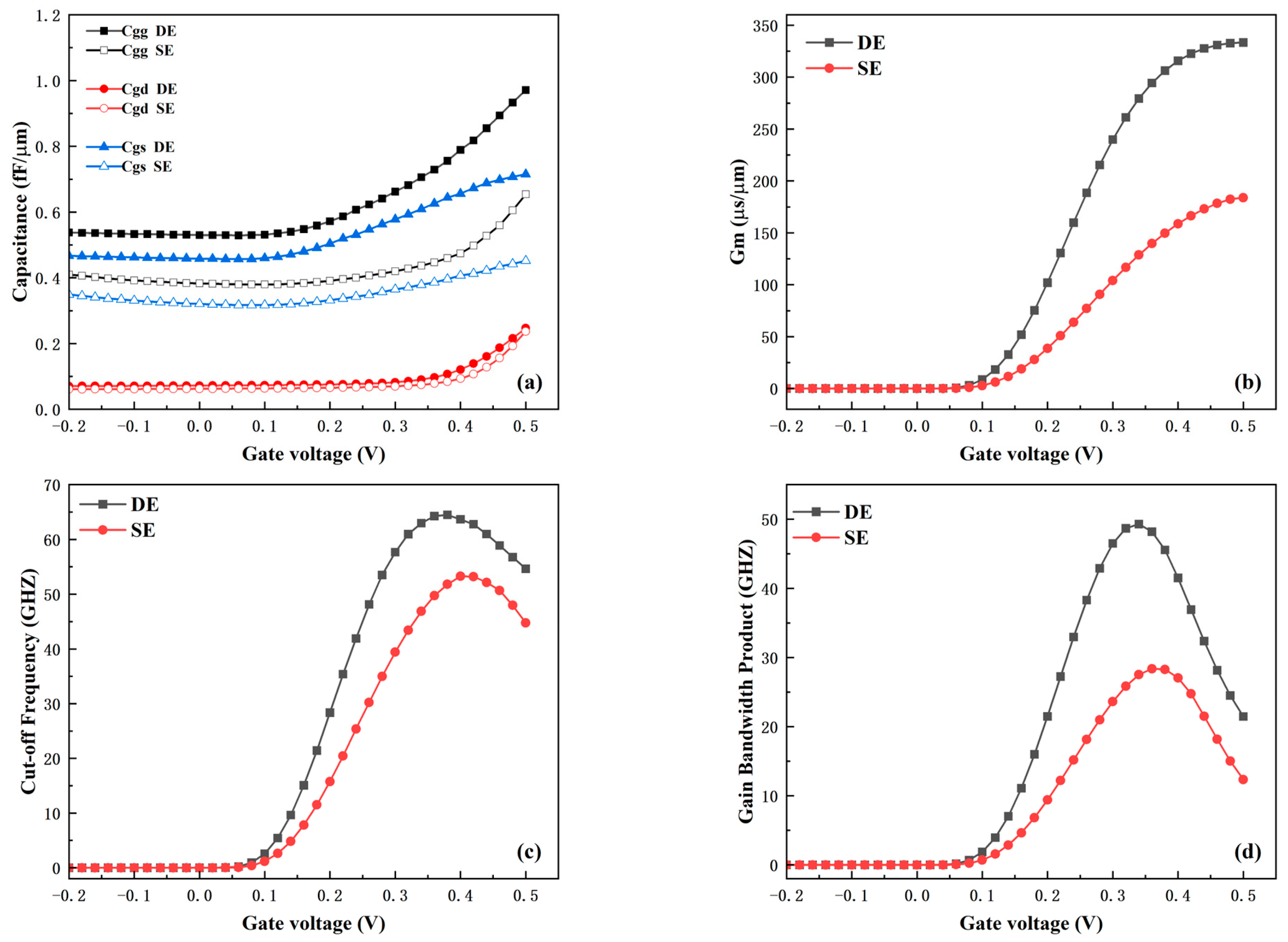
3.4. Optimization of the Dual-Electrode Structure
4. Conclusions
Author Contributions
Funding
Data Availability Statement
Conflicts of Interest
References
- Ahn, D.-H.; Yoon, S.-H.; Kato, K.; Fukui, T. Takenaka and S. Takagi. Effects of ZrO2/Al2O3 Gate-Stack on the Performance of Planar-Type InGaAs TFET. IEEE Trans. Electron Devices 2019, 66, 1862–1867. [Google Scholar] [CrossRef]
- Kim, J.H.; Kim, S.; Park, B.-G. Double-Gate TFET with Vertical Channel Sandwiched by Lightly Doped Si. IEEE Trans. Electron Devices 2019, 66, 1656–1661. [Google Scholar] [CrossRef]
- Seabaugh, A.C.; Zhang, Q. Low-Voltage Tunnel Transistors for Beyond CMOS Logic. Proc. IEEE 2010, 98, 2095–2110. [Google Scholar] [CrossRef]
- Dash, S.; Sahoo, G.S.; Mishra, G.P. Subthreshold swing minimization of cylindrical tunnel FET using binary metal alloy gate. Superlattices Microstruct. 2016, 91, 105–111. [Google Scholar] [CrossRef]
- Maurya, A.; Koley, K.; Mech, B.C.; Kumar, J.; Kumar, P. Investigation of Source Region’s Random Doping Fluctuation Effects on Analog and RF Performance in All-Si DG-TFET. IEEE Trans. Electron Devices 2022, 69, 5330–5336. [Google Scholar] [CrossRef]
- Damrongplasit, N.; Kim, S.H.; Liu, T.-J.K. Study of Random Dopant Fluctuation Induced Variability in the Raised-Ge-Source TFET. IEEE Electron Device Lett. 2013, 34, 184–186. [Google Scholar] [CrossRef]
- Kumar, M.J.; Janardhanan, S. Doping-Less Tunnel Field Effect Transistor: Design and Investigation. IEEE Trans. Electron Devices 2013, 60, 3285–3290. [Google Scholar] [CrossRef]
- Ashok, T.; Pandey, C.K. Demonstration of a novel Dual-Source Elevated-Channel Dopingless TFET with improved DC and Analog/RF performance. Microelectron. J. 2024, 144, 106071. [Google Scholar] [CrossRef]
- Sharma, S.; Basu, R.; Kaur, B. Temperature Analysis of a Dopingless TFET Considering Interface Trap Charges for Enhanced Reliability. IEEE Trans. Electron Devices 2022, 69, 2692–2697. [Google Scholar] [CrossRef]
- Gupta, A.K.; Raman, A. Performance analysis of electrostatic plasma-based dopingless nanotube TFET. Appl. Phys. A 2020, 126, 573. [Google Scholar] [CrossRef]
- Duan, X.; Zhang, J.; Wang, S.; Li, Y.; Xu, S.; Hao, Y. A High-Performance Gate Engineered InGaN Dopingless Tunnel FET. IEEE Trans. Electron Devices 2018, 65, 1223–1229. [Google Scholar] [CrossRef]
- Choudhary, V.; Agrawal, S.; Kumar, M.; Verma, M. Negative Capacitance Vertical Dopingless TFET and Its Analog/RF Analysis Using Interface Trap Charges. IEEE Trans. Device Mater. Reliab. 2025, 25, 163–172. [Google Scholar] [CrossRef]
- Hueting, R.J.E.; Rajasekharan, B.; Salm, C.; Schmitz, J. The Charge Plasma P-N Diode. IEEE Electron Device Lett. 2008, 29, 1367–1369. [Google Scholar] [CrossRef]
- Tripathy, M.R.; Singh, A.K.; Baral, K.; Singh, P.K.; Jit, S. III-V/Si staggered heterojunction based source-pocket engineered vertical TFETs for low power applications. Superlattices Microstruct. 2020, 142, 106494. [Google Scholar] [CrossRef]
- Shaker, A.; Maged, A.; Elshorbagy, A.; AbouElainain, A.; Elsabbagh, M. Source-all-around tunnel field-effect transistor (SAA-TFET): Proposal and design. Semicond. Sci. Technol. 2020, 35, 025007. [Google Scholar] [CrossRef]
- Zhao, H.; Chen, Y.; Wang, Y.; Zhou, F.; Xue, F.; Lee, J. In0.7Ga0.3As Tunneling Field-Effect Transistors with an Ion of 50 μA/μm and a Subthreshold Swing of 86 mV/dec Using HfO2 Gate Oxide. IEEE Electron Device Lett. 2010, 31, 1392–1394. [Google Scholar] [CrossRef]
- Zhao, H.; Chen, Y.-T.; Wang, Y.; Zhou, F.; Xue, F.; Lee, J.C. Improving the on-current of In0.7Ga0.3As tunneling field-effect-transistors by p++/n+ tunneling junction. Appl. Phys. Lett. 2011, 98, 093501. [Google Scholar] [CrossRef]
- Lu, B.; Cui, Y.; Guo, A.; Wang, D.; Lv, Z.; Zhou, J.; Miao, Y. Characteristics of InAs/GaSb Line-Tunneling FETs with Buried Drain Technique. IEEE Trans. Electron Devices 2021, 68, 1537–1541. [Google Scholar] [CrossRef]
- Sharma, A.; Akkala, A.G.; Kulkarni, J.P.; Roy, K. Source-Underlapped GaSb–InAs TFETs with Applications to Gain Cell Embedded DRAMs. IEEE Trans. Electron Devices 2016, 63, 2563–2569. [Google Scholar] [CrossRef]
- Long, P.; Wilson, E.; Huang, J.Z.; Klimeck, G.; Rodwell, M.J.W.; Povolotskyi, M. Design and Simulation of GaSb/InAs 2D Transmission-Enhanced Tunneling FETs. IEEE Electron Device Lett. 2016, 37, 107–110. [Google Scholar] [CrossRef]
- Yu, T.-Y.; Peng, L.-S.; Lin, C.-W.; Hsin, Y.-M. GaAsSb/InGaAs tunnel field effect transistor with a pocket layer. Microelectron. Reliab. 2018, 83, 235–237. [Google Scholar] [CrossRef]
- Shih, P.-C.; Hou, W.-C.; Li, J.-Y. A U-Gate InGaAs/GaAsSb Heterojunction TFET of Tunneling Normal to the Gate with Separate Control Over ON- and OFF-State Current. IEEE Electron Device Lett. 2017, 38, 1751–1754. [Google Scholar] [CrossRef]
- Liu, H.; Yang, L.-A.; Jin, Z.; Hao, Y. An In0.53Ga0.47As/In0.52Al0.48As Heterojunction Dopingless Tunnel FET with a Heterogate Dielectric for High Performance. IEEE Trans. Electron Devices 2019, 66, 3229–3235. [Google Scholar] [CrossRef]
- Keighobadi, D.; Mohammadi, S.; Mohtaram, M. Switching Performance Investigation of a Gate-All-Around Core-Source InGaAs/InP TFET. Trans. Electr. Electron. Mater. 2021, 22, 502–508. [Google Scholar] [CrossRef]
- Bhattacharyya, A.; Chanda, M.; De, D. GaAs0.5Sb0.5/In0.53Ga0.47As heterojunction dopingless charge plasma-based tunnel FET for analog/digital performance improvement. Superlattices Microstruct. 2020, 142, 106522. [Google Scholar] [CrossRef]
- Gotow, T.; Mitsuhara, M.; Hoshi, T.; Sugiyama, H.; Takenaka, M.; Takagi, S. Effects of impurity and composition profiles on electrical characteristics of GaAsSb/InGaAs hetero-junction vertical tunnel field effect transistors. J. Appl. Phys. 2017, 122, 174503. [Google Scholar] [CrossRef]
- Chen, S.; Wang, S.; Liu, H.; Han, T.; Xie, H.; Chong, C. A Novel Dopingless Fin-Shaped SiGe Channel TFET with Improved Performance. Nanoscale Res. Lett. 2020, 15, 202. [Google Scholar] [CrossRef]
- Mehrad, S.; Yaghobi, H.; Eyvazi, K.; Karami, M.A. Gate Dielectric Engineering Using Stacked Gate Dielectric in U-Shaped Gate Tunnel FET. IET Circuits Devices Syst. 2025, 11, 5014133. [Google Scholar] [CrossRef]
- Xie, H.; Liu, H.; Chen, S.; Han, T.; Wang, S. Electrical performance of InAs/GaAs0.1Sb0.9 heterostructure junctionless TFET with dual-material gate and Gaussian-doped source. Semicond. Sci. Technol. 2020, 35, 095004. [Google Scholar] [CrossRef]
- Apoorva; Kumar, N.; Amin, S.I.; Anand, S. Design and Performance Optimization of Novel Core–Shell Dopingless GAA-Nanotube TFET with Si0.5Ge0.5-Based Source. IEEE Trans. Electron Devices 2020, 67, 789–795. [Google Scholar] [CrossRef]
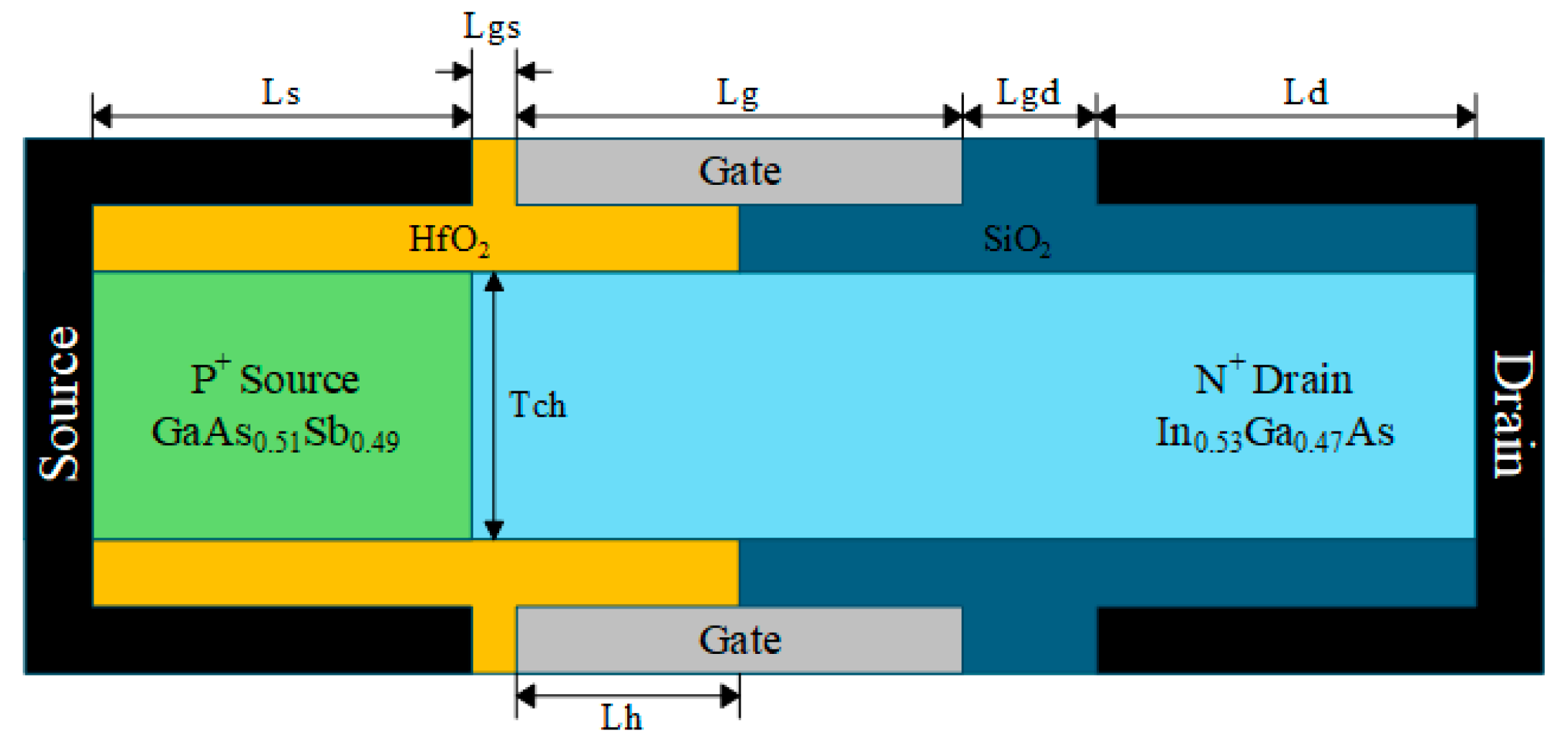
| Parameter Name | Symbol | Value |
|---|---|---|
| Oxide thickness | Tox | 2 nm |
| Channel thickness | Tch | 10 nm |
| Source length | Ls | 50 nm |
| Gate length | Lg | 50 nm |
| Drain length | Ld | 50 nm |
| HfO2 gate dielectric length | Lh | 25 nm |
| Gate-source length | Lgs | 5 nm |
| Gate-drain length | Lgd | 15 nm |
| Gate work function | Wg | 4.7 eV |
| Drain work function | Wd | 4.4 eV |
| Source work function | Ws | 5.0 eV |
| ION (A/μm) | ION/IOFF | fT (GHz) | GBP (GHz) | ||
|---|---|---|---|---|---|
| This work (VGS = 0.5 V) | 8.33 × 10⁻⁵ | 2.44 × 10¹⁰ | 10.18 | 64 | 49 |
| Ref. [7] (VGS = 1.5 V) | 1.1 × 10⁻⁵ | 1.1 × 10¹² | 100 | - | - |
| Ref. [8] (VGS = 2.0 V) | 1.36 × 10⁻⁶ | 1.47 × 10¹¹ | 91 | 0.31 | 0.33 |
| Ref. [21] (VGS = 0.5 V) | 1.2 × 10⁻⁵ | - | 227 | - | - |
| Ref. [23] (VGS = 0.6 V) | 1.67 × 10⁻⁵ | 1.96 × 10⁸ | 36.6 | 13 | 5.23 |
| Ref. [25] (VGS = 0.6 V) | 4.05 × 10⁻⁵ | 4.86 × 10⁹ | 20.3 | 71 | 12 |
| Ref. [27] (VGS = 1.0 V) | 5.88 × 10⁻⁵ | 5.88 × 10¹² | 18.2 | 5.04 | 1.29 |
| Ref. [30] (VGS = 1.0 V) | 1.69 × 10⁻⁵ | 8.46 × 10¹¹ | 31.38 | 36 | - |
Disclaimer/Publisher’s Note: The statements, opinions and data contained in all publications are solely those of the individual author(s) and contributor(s) and not of MDPI and/or the editor(s). MDPI and/or the editor(s) disclaim responsibility for any injury to people or property resulting from any ideas, methods, instructions or products referred to in the content. |
© 2025 by the authors. Licensee MDPI, Basel, Switzerland. This article is an open access article distributed under the terms and conditions of the Creative Commons Attribution (CC BY) license (https://creativecommons.org/licenses/by/4.0/).
Share and Cite
Huang, J.; Liu, H.; Chen, S.; Wang, S.; Chong, C.; Liu, C. Performance Analysis and Optimization of an InGaAs/GaAsSb Heterojunction Dopingless Tunnel FET with a Heterogate Dielectric. Micromachines 2025, 16, 1330. https://doi.org/10.3390/mi16121330
Huang J, Liu H, Chen S, Wang S, Chong C, Liu C. Performance Analysis and Optimization of an InGaAs/GaAsSb Heterojunction Dopingless Tunnel FET with a Heterogate Dielectric. Micromachines. 2025; 16(12):1330. https://doi.org/10.3390/mi16121330
Chicago/Turabian StyleHuang, JunJie, HongXia Liu, Shupeng Chen, Shulong Wang, Chen Chong, and Chang Liu. 2025. "Performance Analysis and Optimization of an InGaAs/GaAsSb Heterojunction Dopingless Tunnel FET with a Heterogate Dielectric" Micromachines 16, no. 12: 1330. https://doi.org/10.3390/mi16121330
APA StyleHuang, J., Liu, H., Chen, S., Wang, S., Chong, C., & Liu, C. (2025). Performance Analysis and Optimization of an InGaAs/GaAsSb Heterojunction Dopingless Tunnel FET with a Heterogate Dielectric. Micromachines, 16(12), 1330. https://doi.org/10.3390/mi16121330


