Study on Stress Distribution and Its Impact on Reliability of SiO2-Based Inorganic Chiplet Gap Filling
Abstract
1. Introduction
2. Experimental
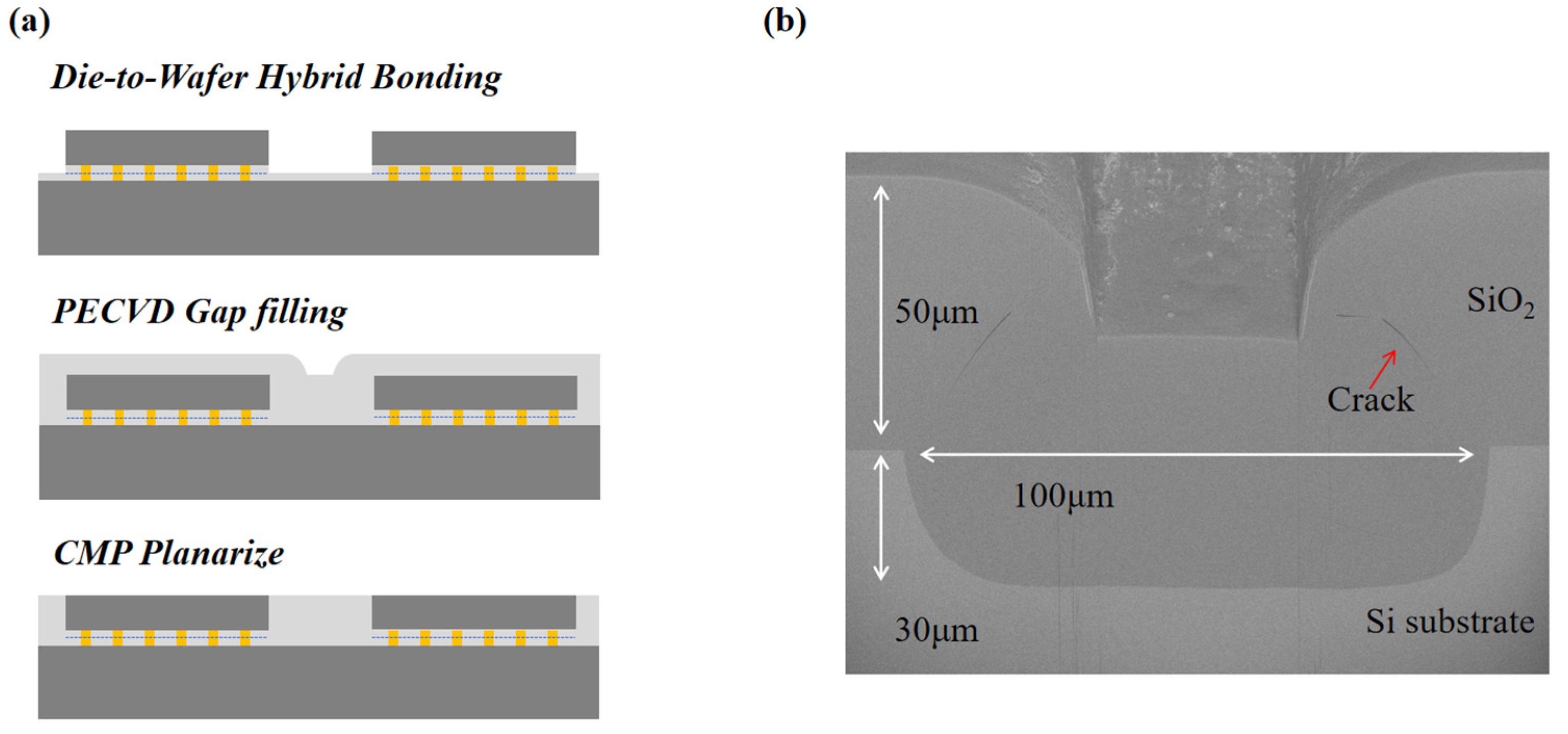
2.1. The Preparation of Gap Filling Samples
2.2. Nanoindentation Tests
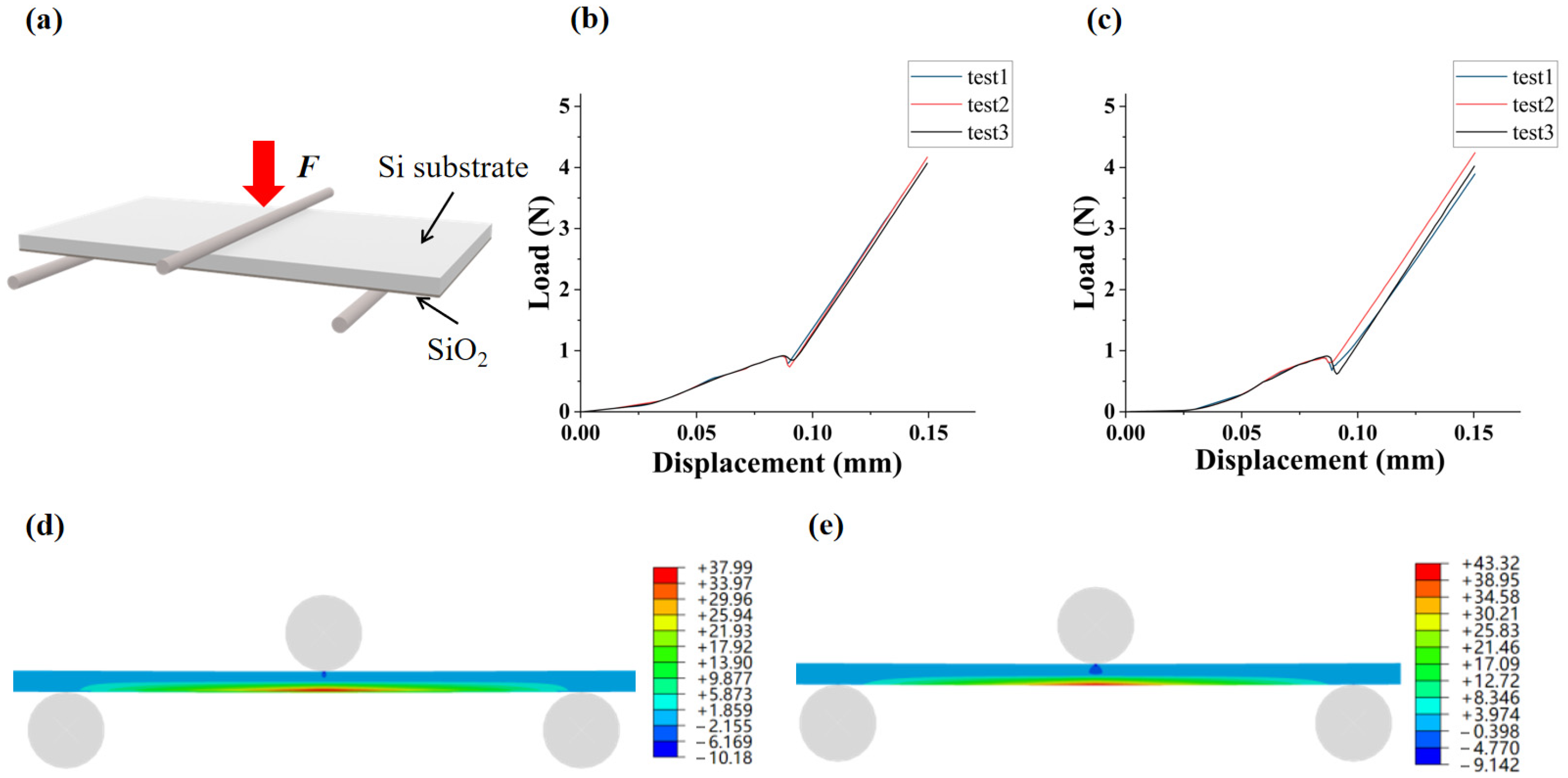
2.3. Three-Point Bending Test
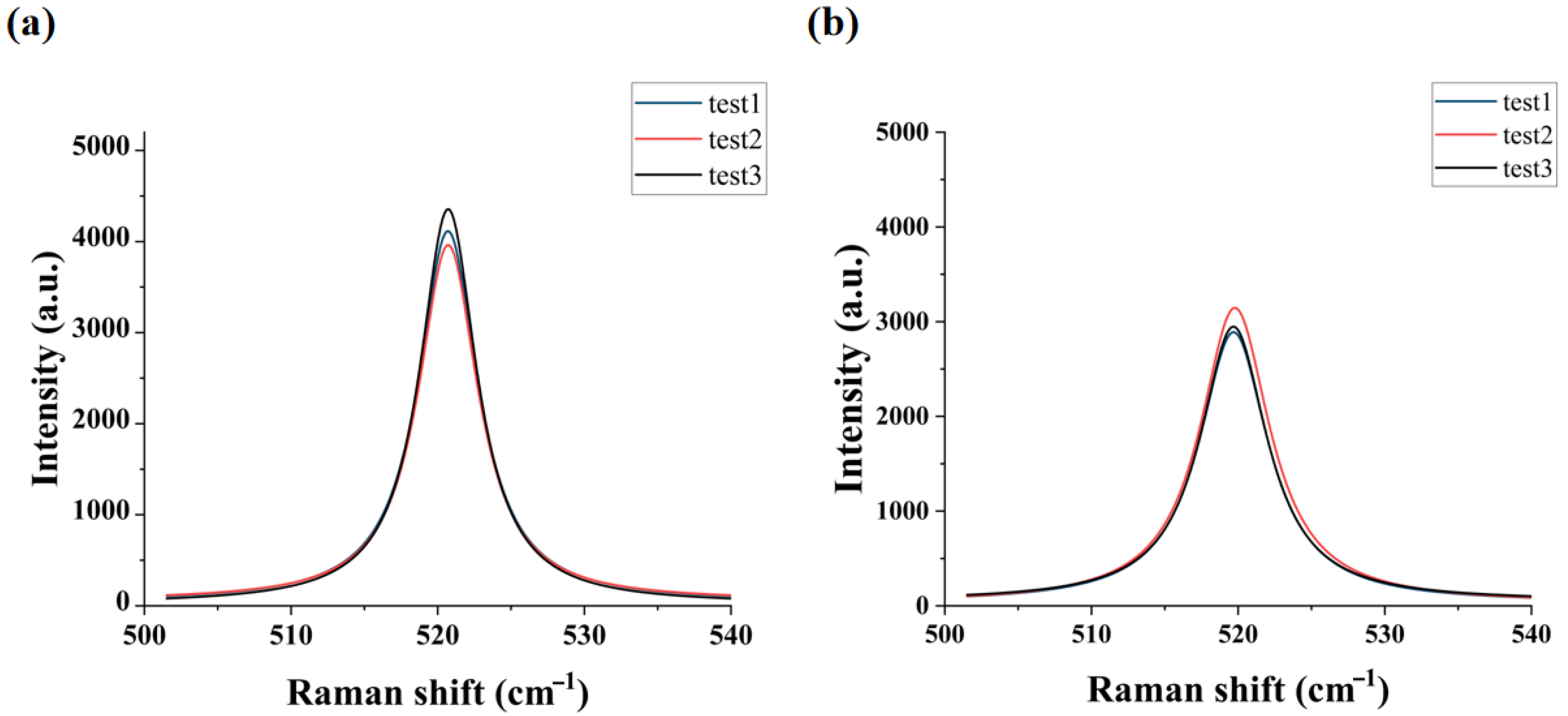
2.4. Polarized Raman Spectroscopy
3. Results and Discussion
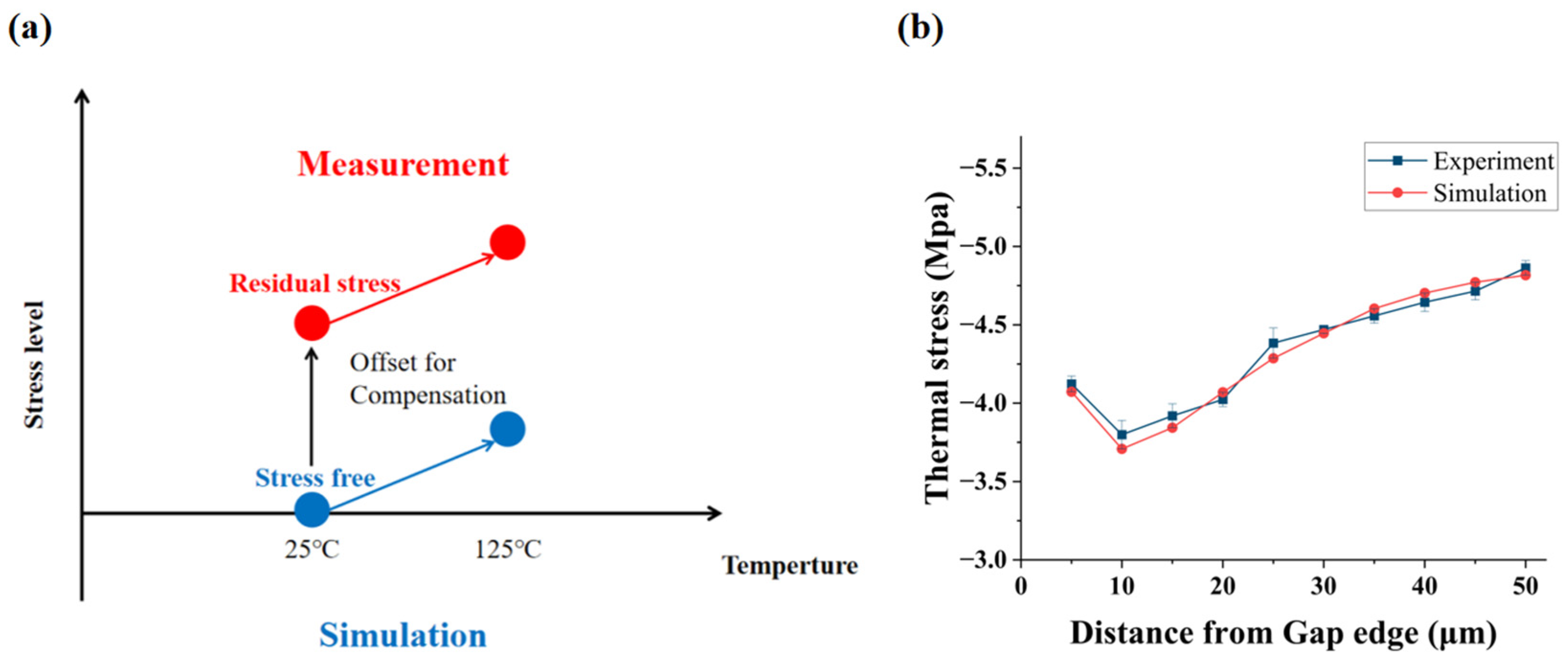
3.1. Validation of the Simulation Was Conducted via Stress Measurement
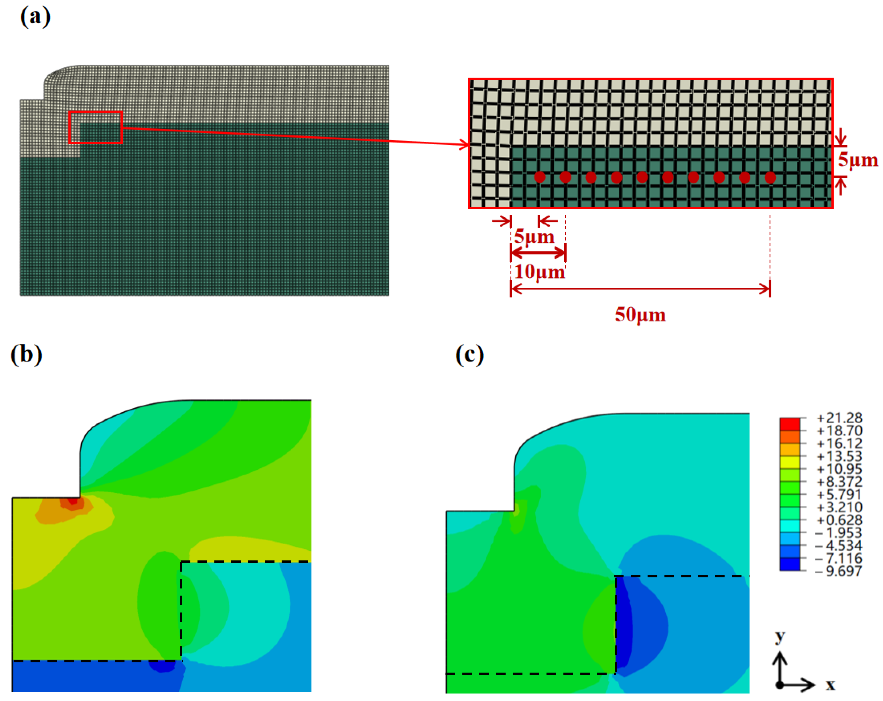
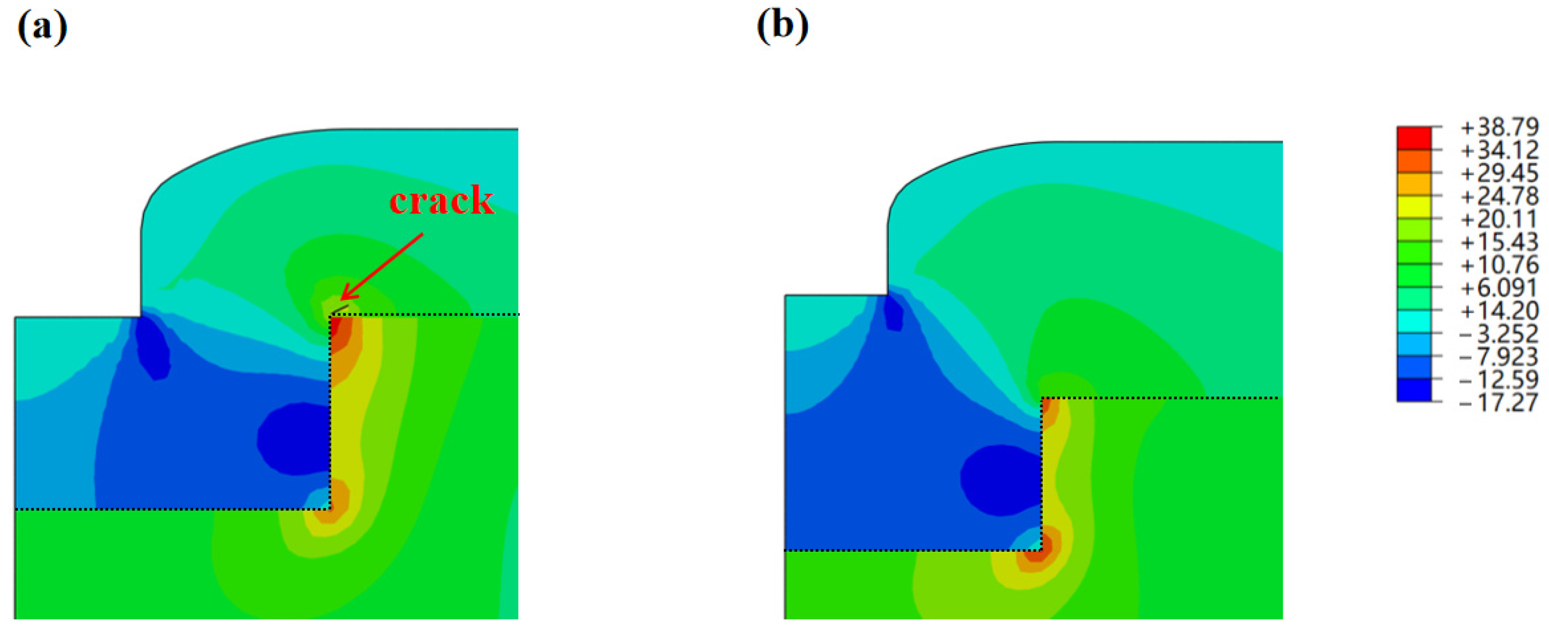
3.2. Simulation of SiO2 Crack Initiation and Propagation via the XFEM
4. Conclusions
Author Contributions
Funding
Data Availability Statement
Conflicts of Interest
References
- Elsherbini, A.; Jun, K.; Liff, S.; Talukdar, T.; Bielefeld, J.; Li, W.; Vreeland, R.; Niazi, H.; Rawlings, B.; Ajayi, T.; et al. Enabling Next Generation 3d Heterogeneous Integration Architectures on Intel Process. In Proceedings of the 2022 International Electron Devices Meeting (IEDM), San Francisco, CA, USA, 3–7 December 2022. [Google Scholar]
- Li, M.J.; Bakir, M.S. 3-D Integrated Chiplet Encapsulation (3-D Ice): High-Density Heterogeneous Integration Using SiO2-Reconstituted Tiers. IEEE Trans. Compon. Packag. Manuf. Technol. 2021, 11, 2242–2245. [Google Scholar] [CrossRef]
- Li, T.; Hou, J.; Yan, J.; Liu, R.; Yang, H.; Sun, Z. Chiplet Heterogeneous Integration Technology—Status and Challenges. Electronics 2020, 9, 670. [Google Scholar] [CrossRef]
- Desai, S.B.; Madhvapathy, S.R.; Sachid, A.B.; Llinas, J.P.; Wang, Q.; Ahn, G.H.; Pitner, G.; Kim, M.J.; Bokor, J.; Hu, C.; et al. Mos2 Transistors with 1-Nanometer Gate Lengths. Science 2016, 354, 99–102. [Google Scholar] [CrossRef] [PubMed]
- Tippabhotla, S.K.; Kumar, M.D.; Sekhar, V.N.; Kumar, C.H.; Rao, B.S.S.C.; Rao, V.S. Digital Design of Inter-Die Gap Fill Dielectric Film Processing for c2w Hybrid Bonding Using Finite Element Modelling. In Proceedings of the 2025 IEEE 75th Electronic Components and Technology Conference (ECTC), Dallas, TX, USA, 27–30 May 2025. [Google Scholar]
- Kumar, M.D.; Sekhar, V.N.; Ling, X.; Kumar, C.H.; Tippabhotla, S.K.; Rao, B.S.S.C.; Tupaen, H.R.; Chong, S.C.; Rao, V.S. Warpage Engineering in C2w Hybrid Bonding Using Inter-Die Gap Fill Dielectrics for 2.5d/3d Integration. In Proceedings of the 2025 IEEE 75th Electronic Components and Technology Conference (ECTC), Grapevine, TX, USA, 27–30 May 2025. [Google Scholar]
- Victor, A.; Manley, M.; Oh, S.; Bakir, M.S. Reconstituted-SiO2 Tier with Integrated Copper Heat Spreader. In Proceedings of the 2023 IEEE 73rd Electronic Components and Technology Conference (ECTC), Orlando, FL, USA, 30 May–2 June 2023. [Google Scholar]
- Wang, T.; Silva, J.L.; Daily, R.; Capuz, G.; Gonzalez, M.; Rebibis, K.J.; Kroehnert, S.; Beyne, E. Wafer Reconstruction: An Alternative 3d Integration Process Flow. In Proceedings of the 2013 IEEE 15th Electronics Packaging Technology Conference (EPTC 2013), Singapore, 11–13 December 2013. [Google Scholar]
- Deng, S.S.; Hwang, S.J.; Lee, H.H. Warpage Prediction and Experiments of Fan-out Waferlevel Package During Encapsulation Process. IEEE Trans. Compon. Packag. Manuf. Technol. 2013, 3, 452–458. [Google Scholar] [CrossRef]
- Che, F.X.; Ho, D.; Ding, M.Z.; Zhang, X. Modeling and Design Solutions to Overcome Warpage Challenge for Fan-out Wafer Level Packaging (Fo-Wlp) Technology. In Proceedings of the 2015 IEEE 17th Electronics Packaging and Technology Conference (EPTC), Singapore, 2–4 December 2015. [Google Scholar]
- Yang, C.Y.; Liu, Y.C.; Chen, K.S.; Yang, T.S.; Wang, Y.C.; Lee, S.S. Process Emulation for Predicting Die Shift and Wafer Warpage in Wafer Reconstitution. In Proceedings of the 2017 18th International Conference on Electronic Packaging Technology (ICEPT), Harbin, China, 16–19 August 2017. [Google Scholar]
- Yang, C.Y.; Chen, K.S.; Yang, T.S. Reconstituted Wafer Deformation Analysis through Whole Process Emulation. IEEE Trans. Device Mater. Reliab. 2020, 20, 172–180. [Google Scholar] [CrossRef]
- Wu, X.; Yang, X.; Ye, J.; Liu, G. Novel Prognostics for Igbts Using Wire-Bond Contact Degradation Model Considering on-Chip Temperature Distribution. IEEE Trans. Power Electron. 2025, 40, 4411–4424. [Google Scholar] [CrossRef]
- Zhao, S.; Yang, X.; Wu, X.; Liu, G. Investigation on Creep-Fatigue Interaction Failure of Die-Attach Solder Layers in Igbts under Power Cycling. IEEE Trans. Power Electron. 2025, 40, 7261–7274. [Google Scholar] [CrossRef]
- Wei, Y.; Yang, X.; Wu, X.; Zhao, S.; Liu, G. Investigation on Reproduction of Igbt Die-Attach Solder Degradation with Finite Element Thermal-Mechanical Simulation. In Proceedings of the 2024 IEEE 10th International Power Electronics and Motion Control Conference (IPEMC2024-ECCE Asia), Chengdu, China, 17–20 May 2024. [Google Scholar]
- Chang, C.; Abe, T.; Esashi, M. Trench Filling Characteristics of Low Stress Teos/Ozone Oxide Deposited by Pecvd and Sacvd. Microsyst. Technol. 2004, 10, 97–102. [Google Scholar] [CrossRef]
- Mizuno, S.; Verma, A.; Lee, P.; Nguyen, B. Improved Gap-Filling Capability of Fluorine-Doped Pecvd Silicon Oxide Thin Films. Thin Solid Film. 1996, 279, 82–86. [Google Scholar] [CrossRef]
- Victor, A.; Bakir, M.S. Tier Transfer of Ultrathin Reconstituted- Sio2 Chiplet Tiers. IEEE Trans. Compon. Packag. Manuf. Technol. 2025, 15, 432–434. [Google Scholar] [CrossRef]
- Hasan, M.M.; Ajayi, T.; Wang, Y.; Liu, P.; Surapaneni, R.; Brun, X.F. Inter-Die Gap-Filling with Varying Aspect Ratio Using Pecvd Oxide for 3d Packaging: Model Prediction and Experimental Validation. In Proceedings of the 2025 IEEE 75th Electronic Components and Technology Conference (ECTC), Grapevine, TX, USA, 27–30 May 2025. [Google Scholar]
- Oliver, W.C.; Pharr, G.M. An Improved Technique for Determining Hardness and Elastic Modulus Using Load and Displacement Sensing Indentation Experiments. J. Mater. Res. 1992, 7, 1564–1583. [Google Scholar] [CrossRef]
- Zhang, Y.F.; Zheng, J.; Yu, J.X.; He, H.T. Impact of Strain Rate on the Hardness and Elastic Modulus of Human Tooth Enamel. J. Mech. Behav. Biomed. Mater. 2018, 78, 491–495. [Google Scholar] [CrossRef] [PubMed]
- Shan, Z.; Sitaraman, S.K. Elastic–Plastic Characterization of Thin Films Using Nanoindentation Technique. Thin Solid Film. 2003, 437, 176–181. [Google Scholar] [CrossRef]
- Porwal, D.; Gupta, A.K.; Pillai, A.M.; Sharma, A.K.; Mukhopadhyay, A.K.; Khan, K.; Dey, A. Simulation of Nanoindentation Experiment on Rf Magnetron Sputtered Nanocolumnar V2O5 Film Using Finite Element Method. Mater. Res. Express 2016, 3, 076407. [Google Scholar] [CrossRef]
- Manjunath, G.L.; Jha, B. Nanoscale Fracture Mechanics of Gondwana Coal. Int. J. Coal Geol. 2019, 204, 102–112. [Google Scholar] [CrossRef]
- Ryu, S.K.; Zhao, Q.; Hecker, M.; Son, H.Y.; Byun, K.Y.; Im, J.; Ho, P.S.; Huang, R. Micro-Raman Spectroscopy and Analysis of near-Surface Stresses in Silicon around through-Silicon Vias for Three-Dimensional Interconnects. J. Appl. Phys. 2012, 111, 063513. [Google Scholar] [CrossRef]
- Hecker, M.; Zhu, L.; Georgi, C.; Zienert, I.; Rinderknecht, J.; Geisler, H.; Zschech, E. Analytics and Metrology of Strained Silicon Structures by Raman and Nano-Raman Spectroscopy. In Proceedings of the Frontiers of Characterization and Metrology for Nanoelectronics, Gaithersburg, MD, USA, 27–29 March 2007. [Google Scholar]
- Chen, K.-S.; Zhang, X.; Lin, S.-Y. Intrinsic Stress Generation and Relaxation of Plasma-Enhanced Chemical Vapor Deposited Oxide During Deposition and Subsequent Thermal Cycling. Thin Solid Films 2003, 434, 190–202. [Google Scholar] [CrossRef]

| Young’s Modulus (GPa) | Maximum Initial Damage Stress (MPa) | Fracture Toughness (MPa·m1/2) | Fracture Energy (J/m2) |
|---|---|---|---|
| 60 | 21 | 0.914 | 13.5 |
| Material | Young’s Modulus (GPa) | Poisson’s Ratio |
|---|---|---|
| Si | 130 | 0.26 |
| SiO2 | 60 | 0.17 |
Disclaimer/Publisher’s Note: The statements, opinions and data contained in all publications are solely those of the individual author(s) and contributor(s) and not of MDPI and/or the editor(s). MDPI and/or the editor(s) disclaim responsibility for any injury to people or property resulting from any ideas, methods, instructions or products referred to in the content. |
© 2025 by the authors. Licensee MDPI, Basel, Switzerland. This article is an open access article distributed under the terms and conditions of the Creative Commons Attribution (CC BY) license (https://creativecommons.org/licenses/by/4.0/).
Share and Cite
Ding, Z.; Liu, S.; Lin, C.; Zheng, T.; Xu, L.; Hu, Q.; Shi, T.; Li, L. Study on Stress Distribution and Its Impact on Reliability of SiO2-Based Inorganic Chiplet Gap Filling. Micromachines 2025, 16, 1310. https://doi.org/10.3390/mi16121310
Ding Z, Liu S, Lin C, Zheng T, Xu L, Hu Q, Shi T, Li L. Study on Stress Distribution and Its Impact on Reliability of SiO2-Based Inorganic Chiplet Gap Filling. Micromachines. 2025; 16(12):1310. https://doi.org/10.3390/mi16121310
Chicago/Turabian StyleDing, Ziyang, Shaowei Liu, Chen Lin, Tianze Zheng, Lihui Xu, Qiuhan Hu, Tailong Shi, and Liyi Li. 2025. "Study on Stress Distribution and Its Impact on Reliability of SiO2-Based Inorganic Chiplet Gap Filling" Micromachines 16, no. 12: 1310. https://doi.org/10.3390/mi16121310
APA StyleDing, Z., Liu, S., Lin, C., Zheng, T., Xu, L., Hu, Q., Shi, T., & Li, L. (2025). Study on Stress Distribution and Its Impact on Reliability of SiO2-Based Inorganic Chiplet Gap Filling. Micromachines, 16(12), 1310. https://doi.org/10.3390/mi16121310


