
Creating Tunable Micro-Optical Components via Photopolymerization 3D Printing Combined with Polymer-Dispersed Liquid Crystals


Abstract
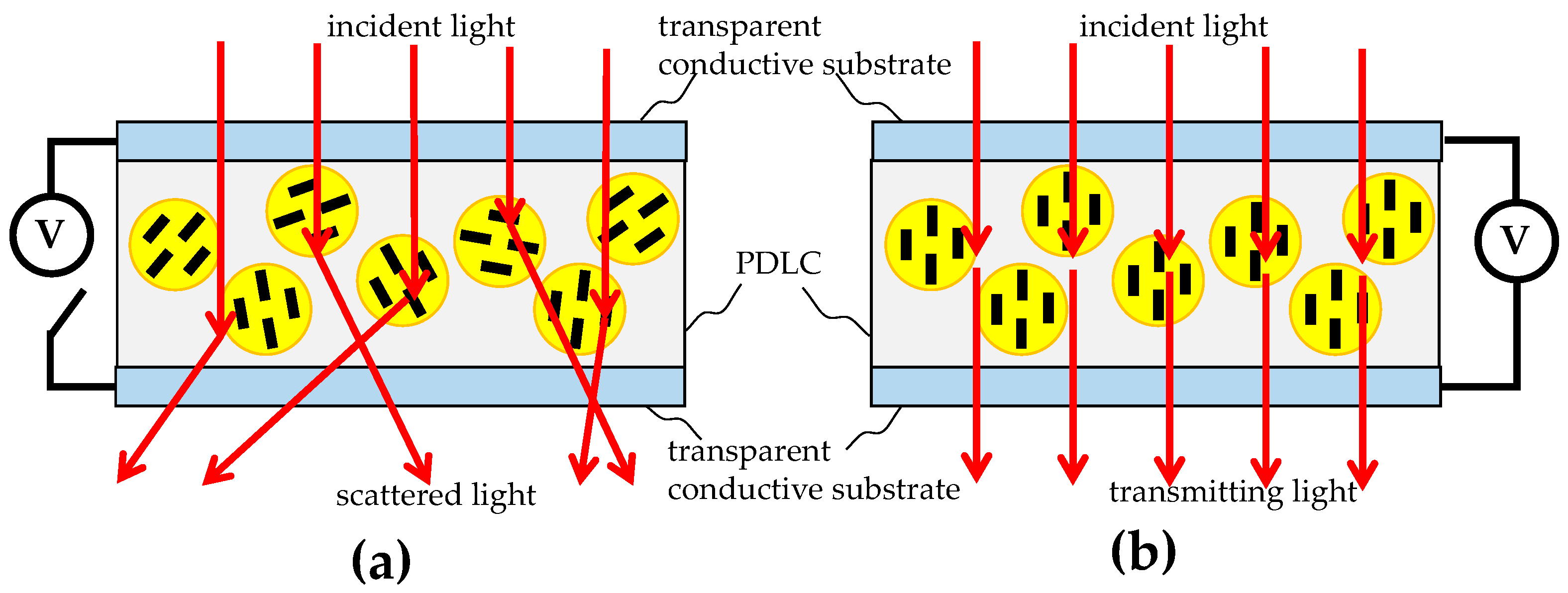
1. Introduction
2. Design and Manufacturing
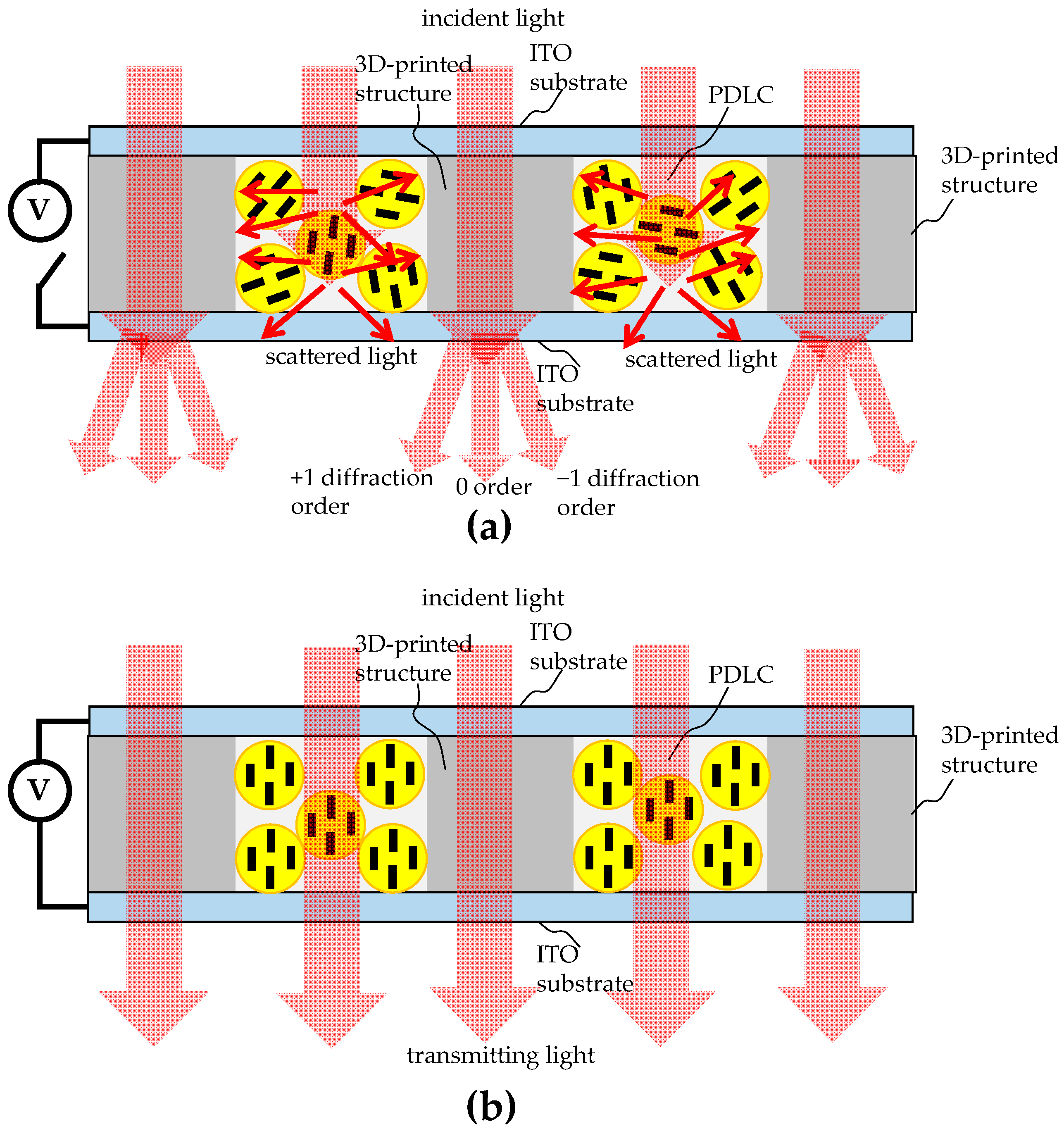
2.1. Design Concept
2.2. Device Design Configuration
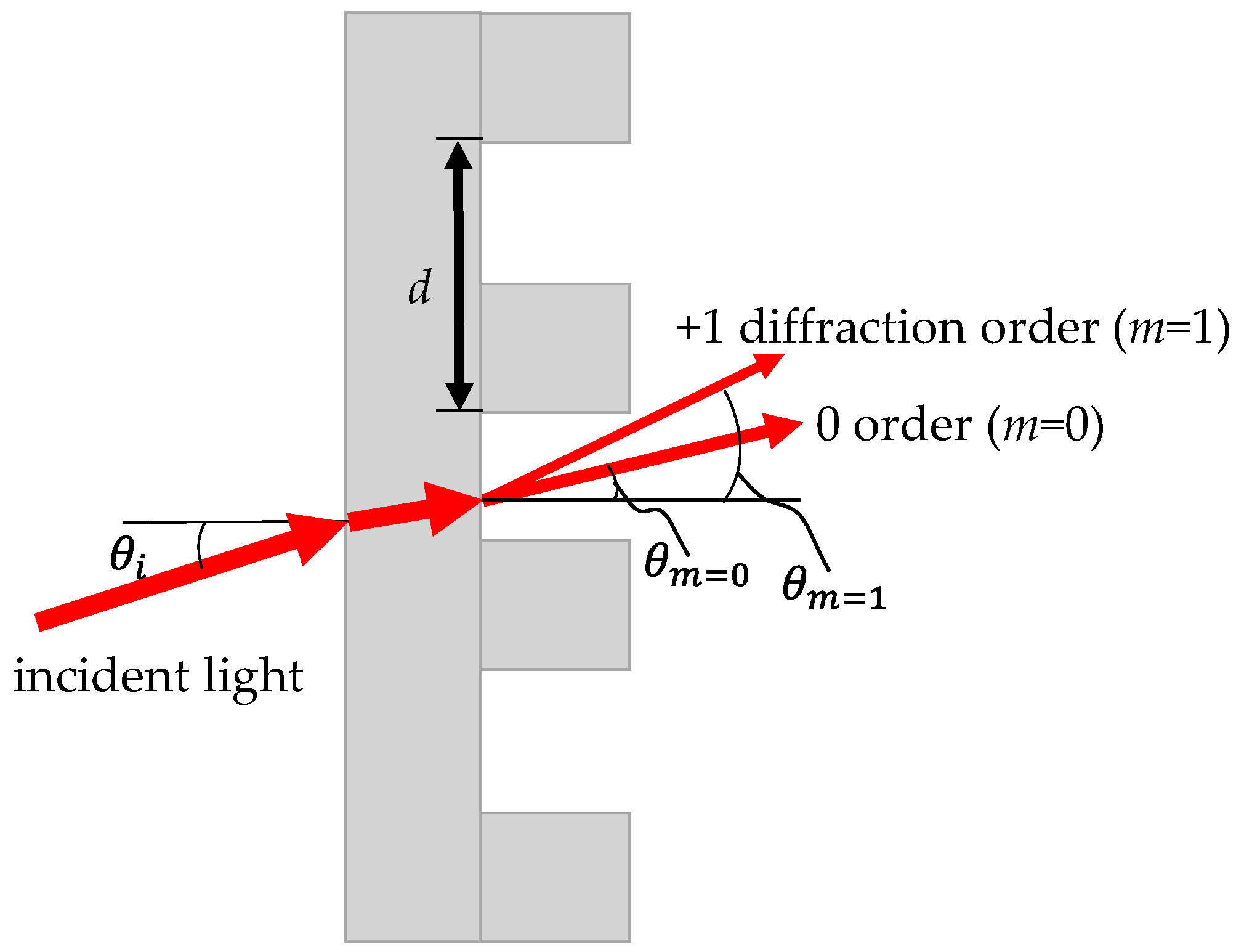
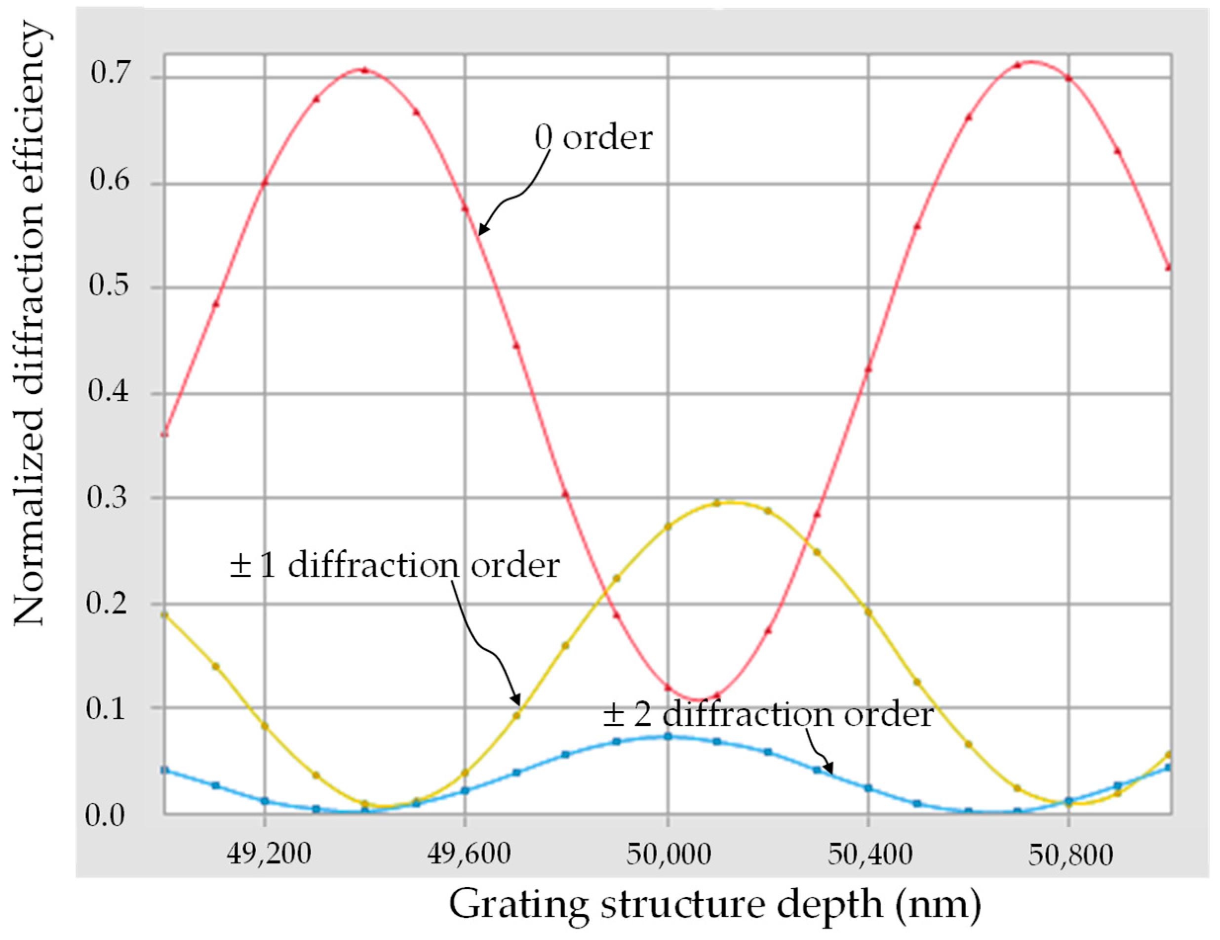
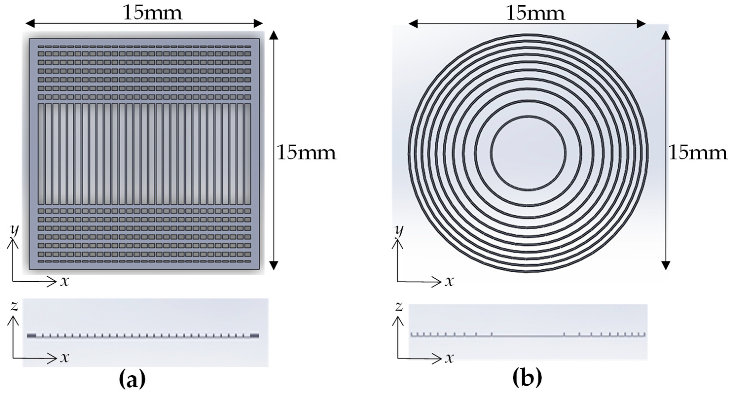
2.2.1. Diffraction Grating
2.2.2. Fresnel Zone Plate
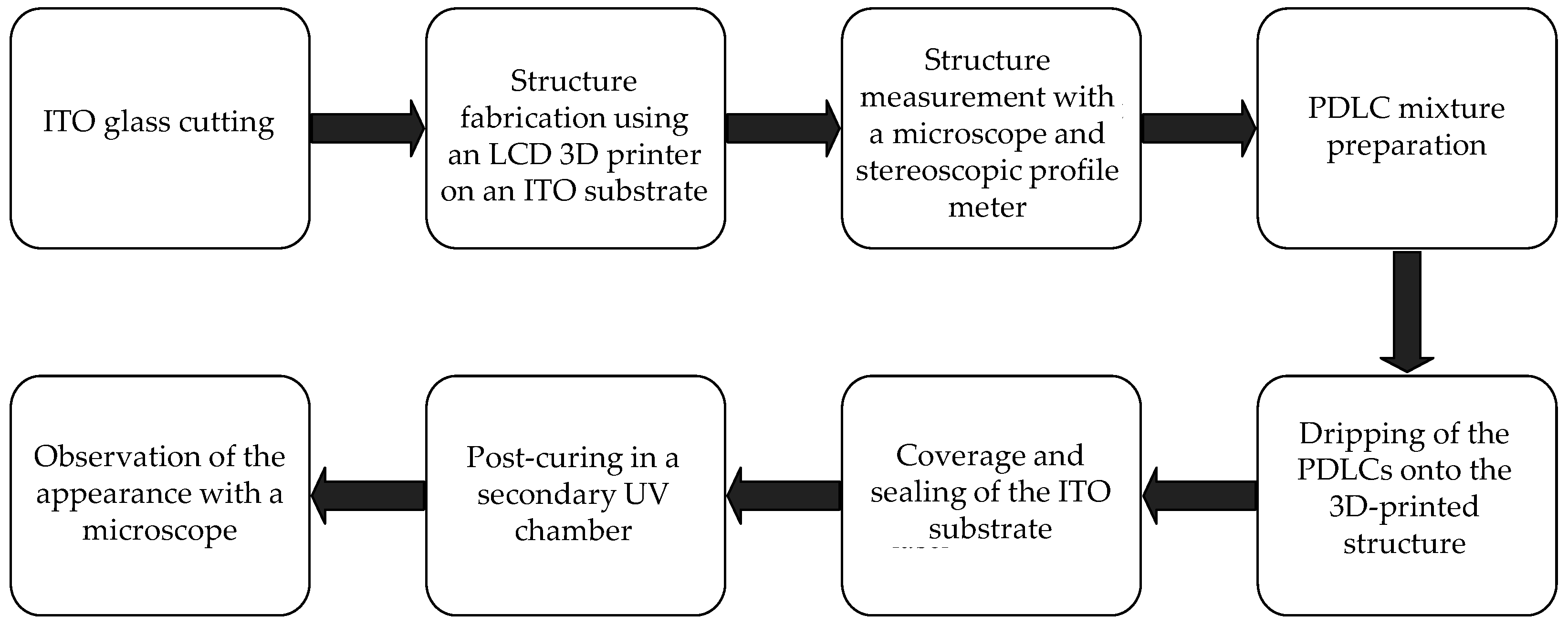
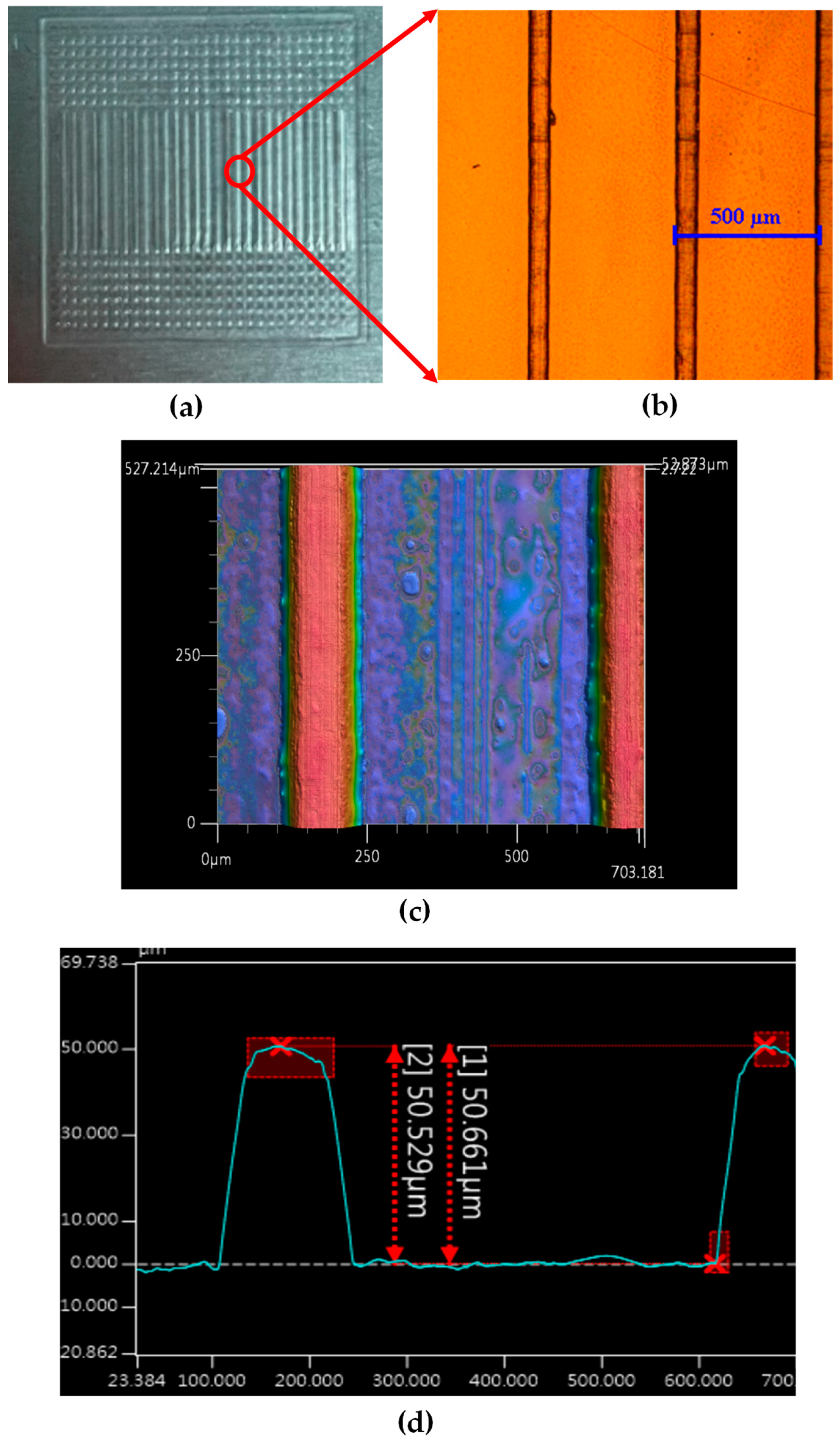
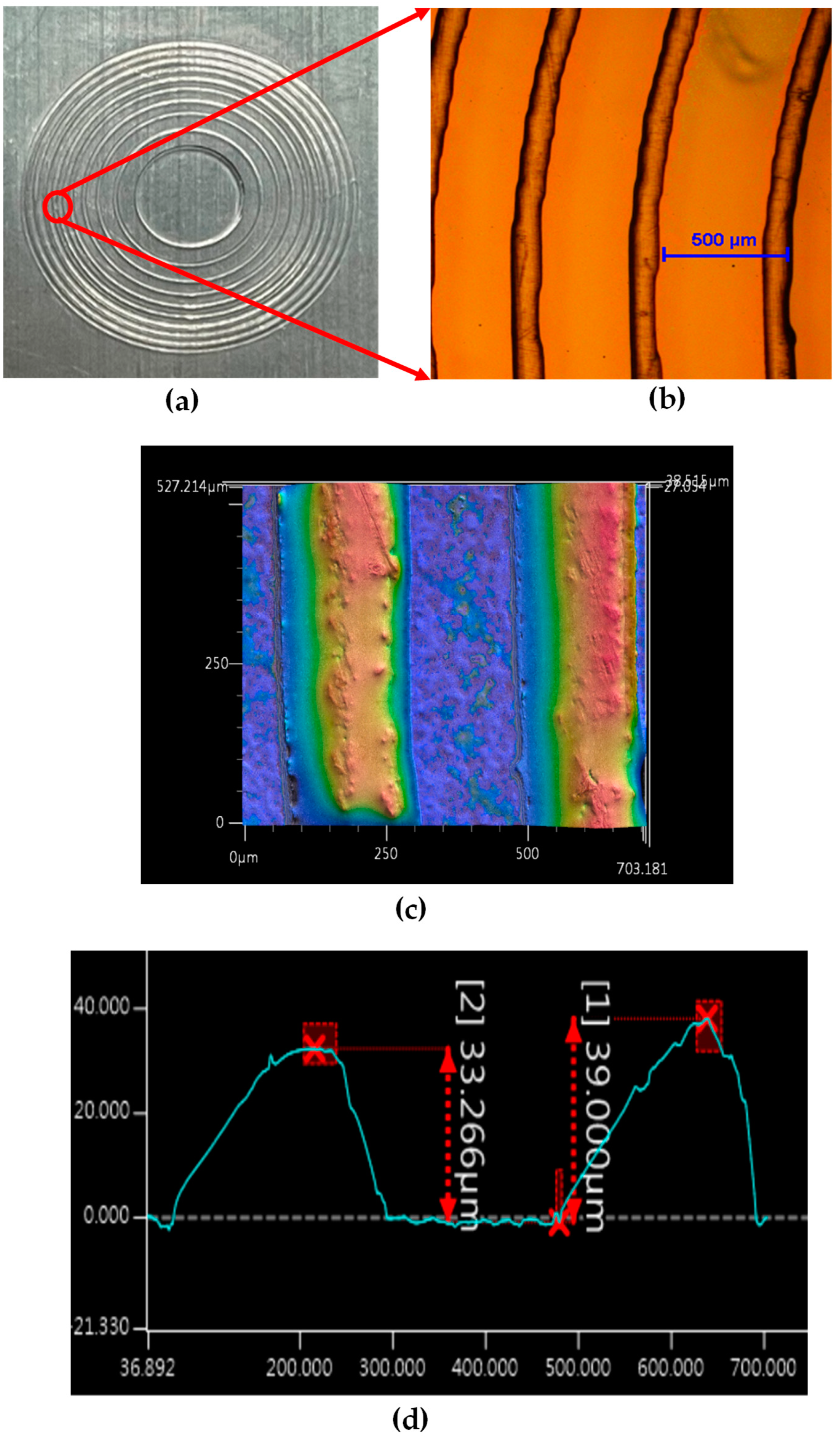
2.3. Manufacturing Results
3. Experiments and Results
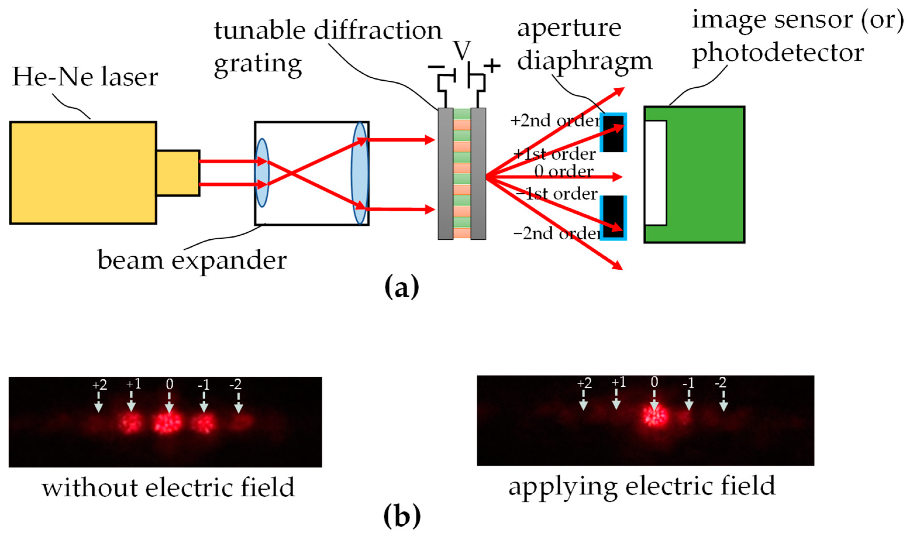
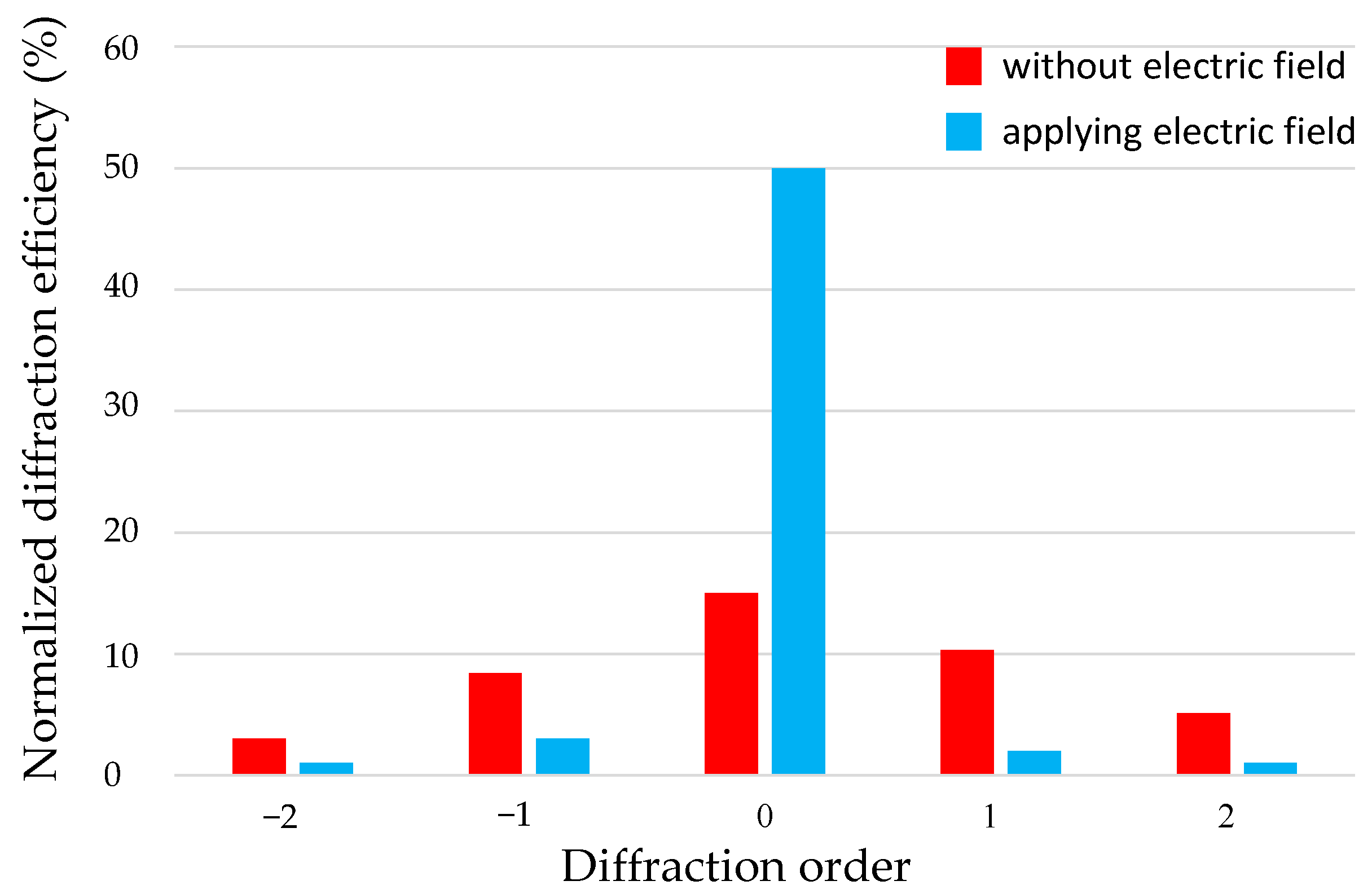
3.1. Diffraction Grating
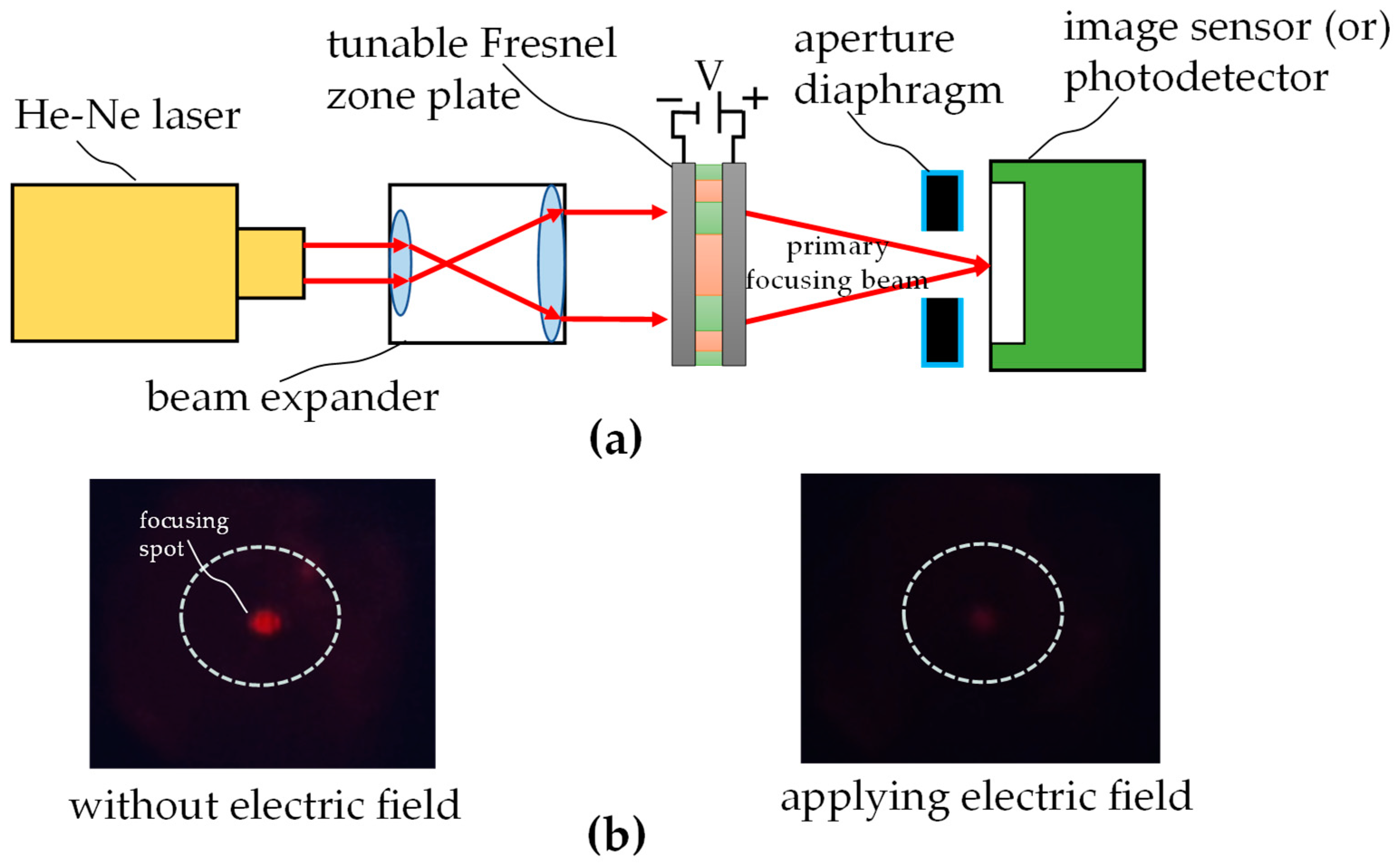
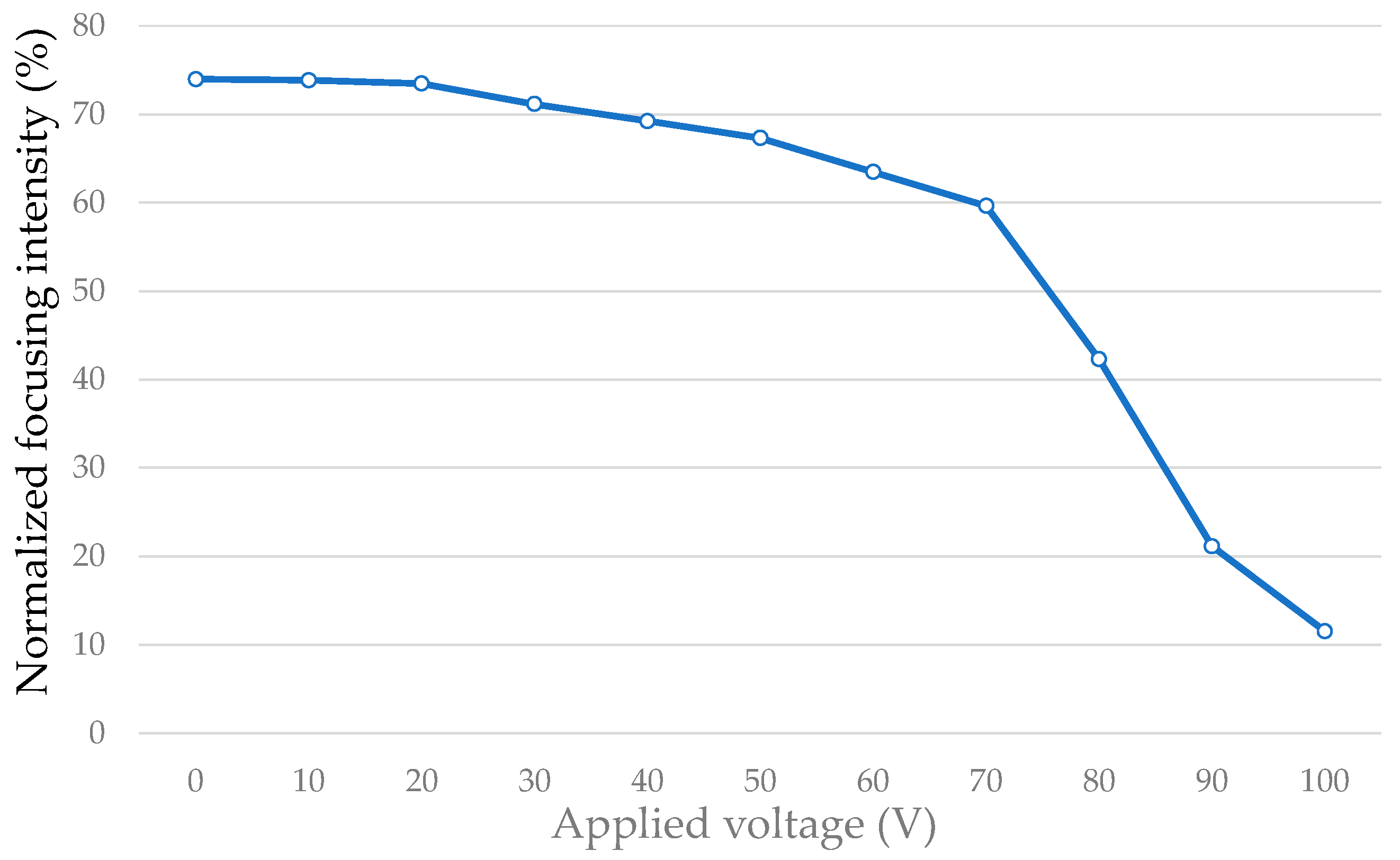
3.2. Fresnel Zone Plate
4. Discussion and Conclusions
Author Contributions
Funding
Data Availability Statement
Acknowledgments
Conflicts of Interest
References
- Sinzinger, S.; Jahns, J. Microoptics; Wiley-VCH: Weinheim, Germany, 2003. [Google Scholar]
- Willis, K.D.D.; Brockmeyer, E.; Hudson, S.E.; Poupyrev, I. Printed Optics: 3D Printing of Embedded Optical Elements for Interactive Devices. In Proceedings of the 25th Annual ACM Symposium on User Interface Software and Technology, Cambridge, MA, USA, 7–10 October 2012; pp. 589–598. [Google Scholar]
- Maillard, P.; Heinrich, A. 3D Printed Freeform Optical Sensors for Metrology Application. In Proceedings of the SPIE-The International Society for Optical Engineering, Jena, Germany, 7–10 September 2015; SPIE: Bellingham, WA, USA, 2015; Volume 9628, p. 96281J-1. [Google Scholar]
- Cook, K.; Canning, J.; Leon-Saval, S.; Reid, Z.; Hossain, M.A.; Comatti, J.E.; Luo, Y.; Peng, G.D. Air-structured optical fiber drawn from a 3D-printed preform. Opt. Lett. 2015, 40, 3966–3969. [Google Scholar] [CrossRef]
- Iezzi, V.L.; Boisvert, J.S.; Loranger, S.; Kashyap, R. 3D printed long period gratings for optical fibers. Opt. Lett. 2016, 41, 1865–1868. [Google Scholar] [CrossRef] [PubMed]
- Juodkazis, S. Manufacturing: 3D printed micro-optics. Nat. Photonics 2016, 10, 499–501. [Google Scholar] [CrossRef]
- Siegle, L.; Ristok, S.; Giessen, H. Complex aspherical singlet and doublet microoptics by grayscale 3D printing. Opt. Express 2023, 31, 4179–4189. [Google Scholar] [CrossRef]
- Kotz, F.; Arnold, K.; Bauer, W.; Schild, D.; Keller, N.; Sachsenheimer, K.; Nargang, T.M.; Richter, C.; Helmer, D.; Rapp, B.E. Three-dimensional printing of transparent fused silica glass. Nature 2017, 544, 337–343. [Google Scholar] [CrossRef] [PubMed]
- Hong, Z.; Ye, P.; Loy, D.A.; Liang, R. Three-dimensional printing of glass micro-optics. Optica 2021, 8, 904–910. [Google Scholar] [CrossRef]
- Aslani, V.; Toulouse, A.; Schmid, M.; Giessen, H.; Haist, T.; Herkommer, A. 3D printing of colored micro-optics. Opt. Mater. Express 2023, 13, 1372–1384. [Google Scholar] [CrossRef]
- Wang, X.; Jiang, M.; Zhou, Z.; Gou, J.; Hui, D. 3D printing of polymer matrix composites: A review and prospective. Compos. Part B Eng. 2017, 110, 442–458. [Google Scholar] [CrossRef]
- Vaidya, N.; Solgaard, O. 3D printed optics with nanometer scale surface roughness. Microsyst. Nanoeng. 2018, 4, 18018. [Google Scholar] [CrossRef] [PubMed]
- Alam, F.; Elsherif, M.; Alqattan, B.; Salih, A.; Lee, S.M.; Yetisen, A.K.; Park, S.; Butt, H. 3D printed contact lenses. ACS Biomater. Sci. Eng. 2021, 7, 794–803. [Google Scholar] [CrossRef] [PubMed]
- Zhu, D.; Zhang, J.; Xu, Q.; Li, Y. 3D printing of customized aspheric lenses for imaging. Polymers 2021, 13, 3477. [Google Scholar] [CrossRef] [PubMed]
- Roper, D.M.; Kwon, K.A.; Malone, L.P.; Best, S.M.; Cameron, R.E. Induced birefringence in 3D printing: Concealing information optically within printed objects. Adv. Mater. 2022, 7, 2200139. [Google Scholar] [CrossRef]
- Deshmukh, K.; Houkan, M.T.; Maadeed, M.A.A.; Sadasivuni, K.K. Introduction to 3D and 4D printing technology: State of the art and recent trends. In 3D and 4D Printing of Polymer Nanocomposite Materials; Elsevier: Amsterdam, The Netherlands, 2018; Chapter 1; pp. 1–25. [Google Scholar]
- Jeong, H.Y.; Lee, E.; An, S.C.; Lim, Y.; Jun, Y.C. 3D and 4D printing for optics and metaphotonics. Nanophotonics 2020, 9, 1139–1160. [Google Scholar] [CrossRef]
- Ali, M.; Alam, F.; Fah, Y.F.; Shiryayev, O.; Vahdati, N.; Butt, H. 4D printed thermochromic Fresnel lenses for sensing applications. Compos. Part B Eng. 2022, 230, 109514. [Google Scholar] [CrossRef]
- Ali, M.; Alam, F.; Butt, H. Fabrication of 5D Fresnel lenses via additive manufacturing. ACS Mater. 2022, 2, 602–613. [Google Scholar] [CrossRef] [PubMed]
- Jung, J.E.; Lee, G.H.; Jang, J.E.; Hwang, K.Y.; Ahmand, F.; Jamil, M.; Woo, L.J.; Jeon, Y.J. Optical property enhancement of dye-PDLC using active reflector structure. Appl. Polym. 2011, 124, 873–877. [Google Scholar] [CrossRef]
- Singh, S.; Srivastava, J.K.; Singh, R.K. Polymer dispersed liquid crystals. In Liquid Crystalline Polymers; Springer: Berlin/Heidelberg, Germany, 2016; Chapter 7; pp. 195–250. [Google Scholar]
- He, Z.; Wu, S.T. Passive polymer-dispersed liquid crystal enabled multi-focal plane displays. Opt. Express 2020, 28, 15294–15299. [Google Scholar] [CrossRef] [PubMed]
- Wu, K.; Sun, J.J.; Meng, F.; Fan, M.; Kong, X.; Cai, M.; Zhao, T.; Yang, C.Y.; Xin, Y.; Xing, J.X.H.; et al. Highly flexible and electrically controlled grating enabled by polymer dispersed liquid crystal. J. Mol. Liq. 2022, 353, 118664. [Google Scholar] [CrossRef]
- Zhang, Z.; He, X.; Zhang, L.; Xu, J.J.; Yuan, B.H.; Chen, C.; Zou, C.; Wang, Q.; Gao, Y.Z.; Yu, M.; et al. A novel low-voltage fast-response electrically controlled dimming film based on fluorinated PDLC for smart window applications. Chem. Eng. J. 2024, 479, 147668. [Google Scholar] [CrossRef]
- Hecht, E. Optics, 4th ed.; Addison-Wesley: San Francisco, CA, USA, 2002; pp. 443–518. [Google Scholar]
- Gsolver Rigorous Diffraction Grating Analysis Software. Available online: http://gsolver.com/products/index.html (accessed on 20 November 2024).
- Ansys Zemax OpticStudio Comprehensive Optical Design Software. Available online: https://www.ansys.com/products/optics/ansys-zemax-opticstudio (accessed on 20 November 2024).
- Phrozen Sonic Mini 8K Resin 3D Printer. Available online: https://phrozen3d.com/products/sonic-mini-8k (accessed on 20 November 2024).
- Chitubox SLA/DLP/LCD 3D Slicer Software. Available online: https://www.chitubox.com/en/index (accessed on 24 December 2024).


| Parameters | Wavelength (nm) | Incident Angle (°) | Index of Refraction (Polymer) | Index of Refraction (Outside) | Grating Period (μm) | Duty Cycle |
|---|---|---|---|---|---|---|
| Value | 632.8 | 0 | 1.5 | 1 | 500 | 25% |
| Zone Radius | ||||||||||
|---|---|---|---|---|---|---|---|---|---|---|
| Value (mm) | 2.249 | 3.181 | 3.897 | 4.499 | 5.031 | 5.511 | 5.951 | 6.364 | 6.749 | 7.115 |
| Parameter | Structure Resolution | Layer Thickness | Exposure Time | Pull Speed |
|---|---|---|---|---|
| Value | 22 μm | 50 μm | 13 sec. | 10 mm/min. |
| Applied voltage (V) | 0 | 10 | 20 | 30 | 40 | 50 |
| Focusing intensity | 74% | 74% | 74% | 71% | 69% | 67% |
| Applied voltage (V) | 60 | 70 | 80 | 90 | 100 | |
| Focusing intensity | 63% | 60% | 42% | 21% | 12% |
Disclaimer/Publisher’s Note: The statements, opinions and data contained in all publications are solely those of the individual author(s) and contributor(s) and not of MDPI and/or the editor(s). MDPI and/or the editor(s) disclaim responsibility for any injury to people or property resulting from any ideas, methods, instructions or products referred to in the content. |
© 2024 by the authors. Licensee MDPI, Basel, Switzerland. This article is an open access article distributed under the terms and conditions of the Creative Commons Attribution (CC BY) license (https://creativecommons.org/licenses/by/4.0/).
Share and Cite
Zhang, S.-Y.; Shih, H.-F.; Tien, C.-L.; Tu, H.-Y. Creating Tunable Micro-Optical Components via Photopolymerization 3D Printing Combined with Polymer-Dispersed Liquid Crystals. Micromachines 2025, 16, 26. https://doi.org/10.3390/mi16010026
Zhang S-Y, Shih H-F, Tien C-L, Tu H-Y. Creating Tunable Micro-Optical Components via Photopolymerization 3D Printing Combined with Polymer-Dispersed Liquid Crystals. Micromachines. 2025; 16(1):26. https://doi.org/10.3390/mi16010026
Chicago/Turabian StyleZhang, Sheng-Yuan, Hsi-Fu Shih, Chuen-Lin Tien, and Han-Yen Tu. 2025. "Creating Tunable Micro-Optical Components via Photopolymerization 3D Printing Combined with Polymer-Dispersed Liquid Crystals" Micromachines 16, no. 1: 26. https://doi.org/10.3390/mi16010026
APA StyleZhang, S.-Y., Shih, H.-F., Tien, C.-L., & Tu, H.-Y. (2025). Creating Tunable Micro-Optical Components via Photopolymerization 3D Printing Combined with Polymer-Dispersed Liquid Crystals. Micromachines, 16(1), 26. https://doi.org/10.3390/mi16010026