Communication

Understanding Quasi-Static and Dynamic Characteristics of Organic Ferroelectric Field Effect Transistors

1
School of Electronics and Information Technology, Sun Yat-sen University, Guangzhou 510275, China
2
Institute of Chemistry Chinese Academy of Sciences, Beijing 100190, China
3
College of Electronic Engineering, South China Agricultural University, Guangzhou 510642, China
4
College of Optical Science and Engineering, Zhejiang University, Hangzhou 310027, China
*
Authors to whom correspondence should be addressed.
Micromachines 2024, 15(4), 467; https://doi.org/10.3390/mi15040467
Submission received: 10 March 2024 / Revised: 23 March 2024 / Accepted: 26 March 2024 / Published: 29 March 2024
(This article belongs to the Special Issue Thin-Film Transistors: Materials, Fabrications and Applications)

Abstract

:
Leveraging poly(vinylidene fluoride-trifluoroethylene) [(PVDF-TrFE)] as the dielectric, we fabricated organic ferroelectric field-effect transistors (OFe-FETs). These devices demonstrate quasi-static transfer characteristics that include a hysteresis window alongside transient phenomena that bear resemblance to synaptic plasticity-encapsulating excitatory postsynaptic current (EPSC) as well as both short-term and long-term potentiation (STP/LTP). We also explore and elucidate other aspects such as the subthreshold swing and the hysteresis window under dynamic state by varying the pace of voltage sweeps. In addition, we developed an analytical model that describes the electrical properties of OFe-FETs, which melds an empirical formula for ferroelectric polarization with a compact model. This model agrees well with the experimental data concerning quasi-static transfer characteristics, potentially serving as a quantitative tool to improve the understanding and design of OFe-FETs.

1. Introduction

Organic ferroelectric field-effect transistors (OFe-FETs) have attracted more research attention due to their prowess in memory-based operations and the advantages of organic materials. They rely on the ferroelectric layer that can be switched between two stable polarization states. Depending on the polarization orientation, charges are induced at the ferroelectric/semiconductor interface and thus impact the channel current. As a three-terminal device, the channel conductance of Fe-FETs can be modulated via the gate and drain terminals, offering the advantage of concurrently actualizing processing and memory functions. In particular, Fe-FETs enable synapse characteristics like LTP, STP, and EPSC that have been demonstrated based on the voltage-controllable polarization reversal. By modulating the pulse inputs, the ferroelectric polarization can be influenced and the operation of a synapse can be successfully mimicked. Yan et al. demonstrated a P(VDF-TrFE)-based OFe-FET synapse with MoS2 as a semiconductor material [1]. Oh et al. achieved 32 levels of conductance states by using a hafnium–zirconium–oxide ferroelectric material [2]. Sun et al. achieved a recognition rate of 98.3% for the MNIST pattern dataset with a 2T-1FeFET design [3].
Extensive research efforts have been made to construct ferroelectric transistors from a material engineering perspective, but the compact modeling of device operation is equally important. To date, most of the existing descriptions of the characteristic behavior of ferroelectric transistors are based on inorganic ferroelectrics such as Hf0.5Zr0.5O2 (HZO) and Pb(Zr0.5Ti0.8)O3 (PZT) [4,5,6,7]. Wang et al. explained the HZO-based device using a calibrated ferroelectric (FE) switching model [4]. Pahwa et al. explained the behavior of PZT-based transistors using a negative capacitance model [5]. However, compact models of ferroelectric transistors based on organic ferroelectric (mainly PVDF polymer) and organic semiconductors remain elusive.
Here, we fabricated the OFe-FET based on a P(VDF-TrFE) polymer and the organic semiconductor material dioctylbenzothienobenzothiophene (C8-BTBT) with a typical hysteresis window depending on gate sweeping. By modulating the sweeping rate of gate voltage, transfer characteristics under quasi-static and dynamic conditions are demonstrated. We also present the compact model for OFe-FETs by considering the ferroelectric polarization effect within organic ferroelectric materials and the disordered charge transport within organic semiconductors. The compact model generally well describes the experimental results concerning quasi-static characteristics and can capture the core aspects of device performance. Additionally, synaptic behavior under pulse inputs is successfully mimicked with the devices.

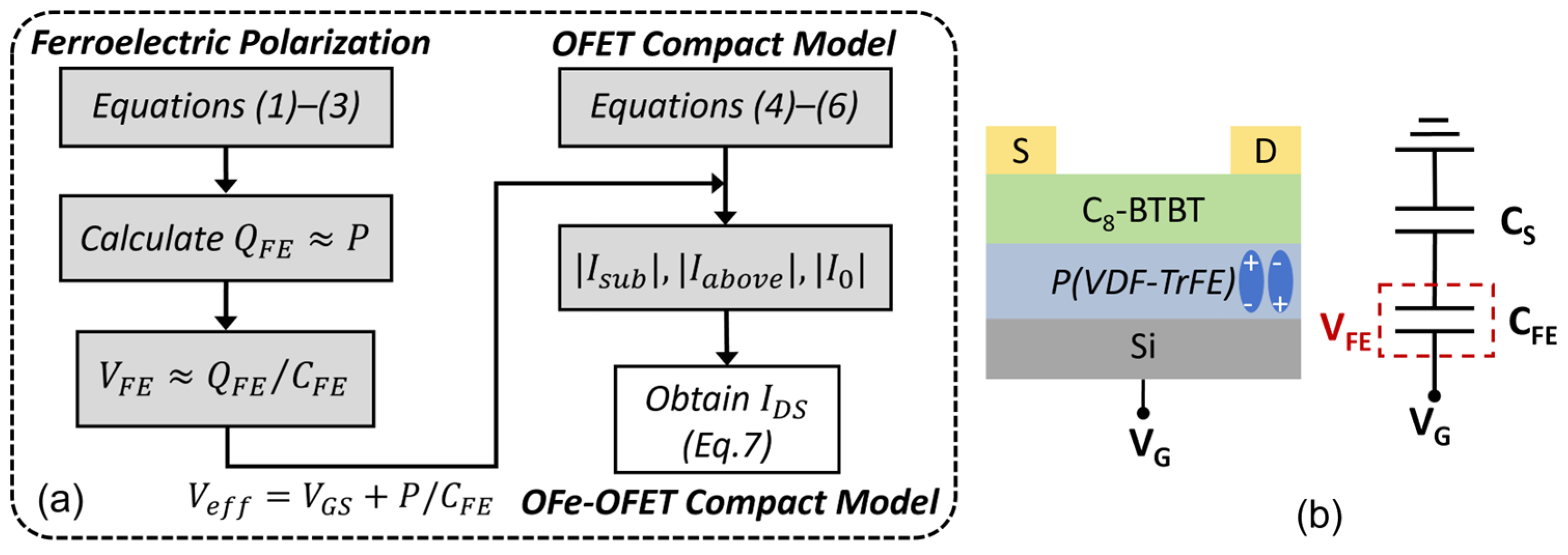
2. Device Fabrication

Experimental OFe-FET devices with P(VDF-TrFE) (Sigma-Aldrich, Saint Louis, MO, USA) as the ferroelectric materials, C8-BTBT as the semiconductors, silicon substrate as the gate electrode and MoO3/Au (5 nm/60 nm) as the drain and source electrodes are shown in Figure 1a. P(VDF-TrFE) films were deposited on the heavily p-doped silicon substrate by spin coating using a solution of 50 mg/mL P(VDF-TrFE) 70/30 mol% dissolved in dimethylformamide (DMF), which was followed by drying and annealing at 135 °C for 2 h in N2 atmosphere. The C8-BTBT layer was then thermally evaporated with a thickness of 40 nm. Finally, MoO3 and Au (5/50 nm) were deposited by thermal evaporation to define the source and drain electrodes. The capacitance of the ferroelectric layer was measured by applying the AC voltage (frequency = 1 kHz) on the capacitor using a Precision LCR Meter E4980A (Agilent Technologies Inc., Santa Clara, CA, USA). The transfer characteristics of the OFe-FETs were measured using a semiconductor analyzer (B1500A, Agilent Technologies Inc., Santa Clara, CA, USA).
The microstructure of P(VDF-TrFE) films shows typical randomly distributed needle-like morphology [8] by Atomic Force Microscopy (AFM) in Figure 1b. To further explore the electrical characteristics of the ferroelectric layer, we fabricated the metal-ferroelectric-metal (MFM) sample by using ITO as the bottom electrode, Au as the top electrode and 200 nm P(VDF-TrFE) film as the insulator layer, as shown in Figure 1c. The capacitance measurements were performed on the MFM devices, and the result exhibits strong hysteresis (butterfly shape, Figure 1d), which stems from the polarization reversal in the film as typical ferroelectric properties [9,10].

3. Results and Discussion

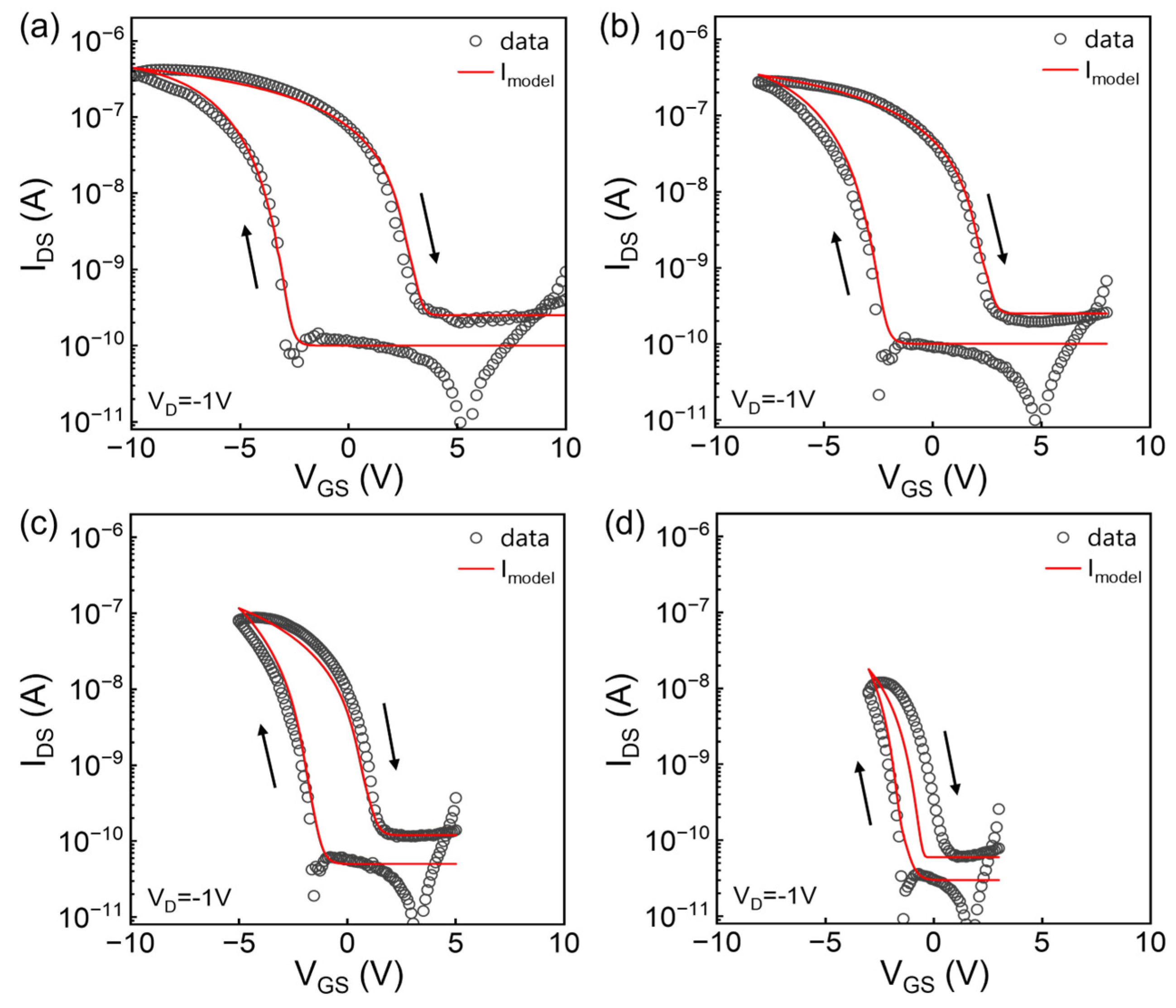
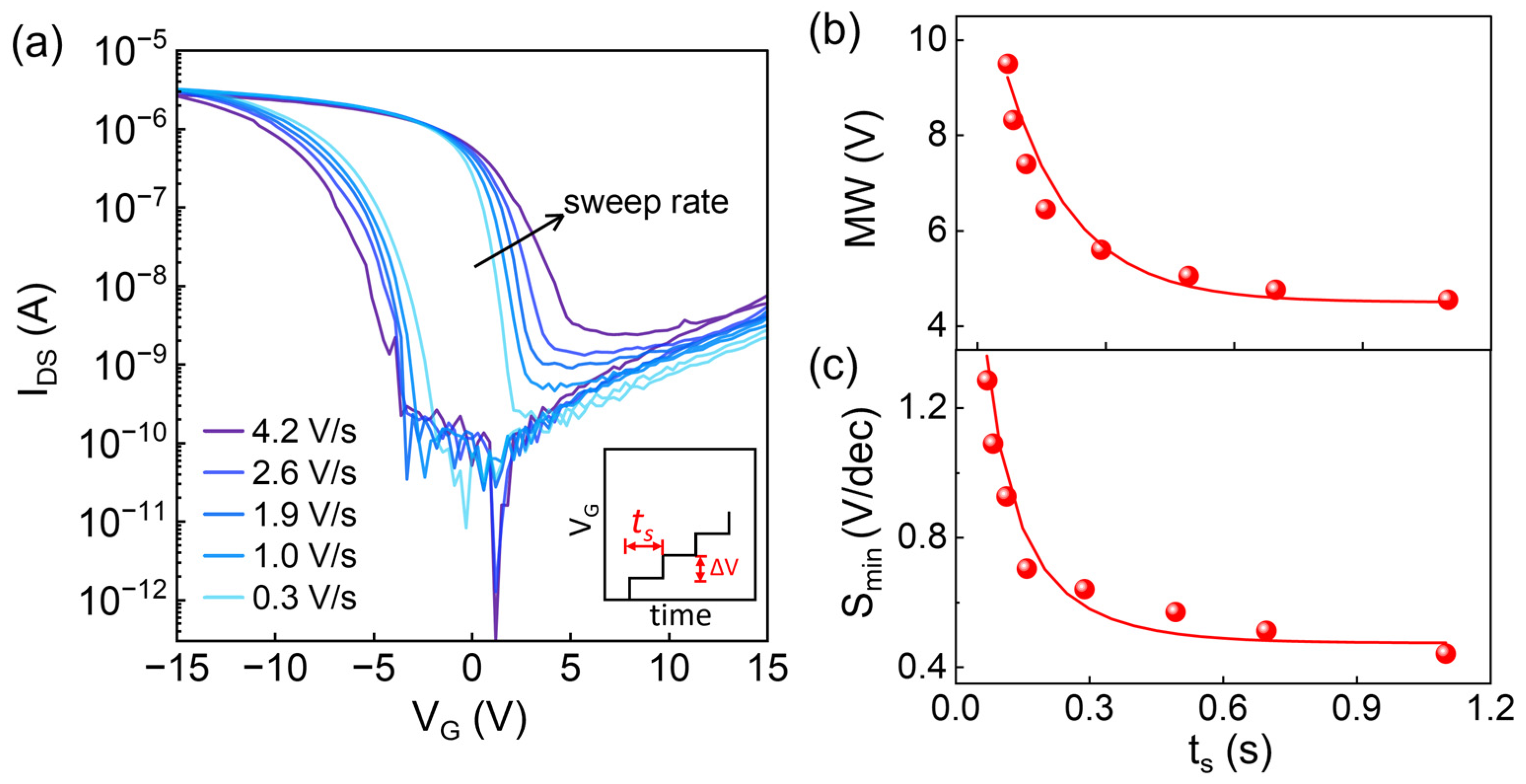
3.1. Quasi-Static Characteristics

The quasi-static transfer characteristics with gate voltage (VG) that sweeps from +3 to −3 V, +5 to −5 V, +8 to −8 V, +10 to −10 V and then backward are shown in Figure 2, operating in the linear region with a drain voltage (VD = −1 V). The current–voltage (IDS-VG) curves exhibit a typical p-type behavior and hysteresis with a clockwise direction, which is consistent with the accumulation and depletion of hole carriers during the switching of ferroelectric polarization. As a p-type device, the drain current reaches the maximum value, which is represented by the current peaks in Figure 2a when VG reaches −3 V, −5 V, −8 V and −10 V, respectively. And the enlarged memory window under higher VG indicates the enhanced polarization of the FE layer and implies the potential for memory application. For memory application, the difference between the threshold voltages (VT) of OFe-FET under different voltage sweeping direction is defined as a memory window (MW) (see Figure 2b). The device exhibits an on/off ratio reaching 104 and obvious memory windows under different sweeping ranges, even at low voltages. The memory widow is 5.9 V at the VG = ±10 V sweeping range, which is comparable to the existing research on OFeFETs [11,12,13]. These results suggest that our device can contribute to the realization of OFe-FET memory devices.
We incorporate the expression of ferroelectric polarization into an analytical current-voltage (I-V) model [14,15] for constructing the compact OFe-FET model. There has been a consensus that the ferroelectric polarization of ferroelectric materials is a function of the electric field [16,17]. The polarization below the applied maximum field can be described as:
P + = P s tan h E E c δ + P s 2 tan h E m a x + E c δ tan h E m a x E c δ
P = P s tan h E + E c δ P s 2 tan h E m a x + E c δ tan h E m a x E c δ
with
δ = 2 E c / ln 1 + P r P s / 1 P r P s
where P or P+ denotes polarization toward negative or positive polarization, E is the applied electric field, Pr is the remanent polarization at the zero applied field, Ps is the saturation polarization, Ec is the coercive field at which the polarization changes the sign, and Emax is the maximum applied electric field and δ is the calculated constant.
For OFETs, the I-V relations are defined by connecting the above-threshold Iabove, subthreshold Isub, and off regimes. By including a contact voltage drop, the above-threshold current Iabove is written as [15]:
I a b o v e = W L μ C i ( V G S V T ) 1 + W L μ C i R c ( V G S V T ) × V D S 1 + V D S α s ( V G S V T ) m 1 m × 1 λ V D S
where W and L are the channel width and length, Ci is the insulator capacitor per unit area, VT is the threshold voltage, Rc is the contact resistance, λ is induced to improve output conductance fitting, αs models the deviation of the saturation drain voltage VDS from the (VGS-VT) point, and m controls the abruptness of linear-to-saturation transition. The mobility µ is defined by the power-law expression with gate voltage VGS for the disordered charge transport in organic semiconductors [18,19]:
μ = μ 0 V a a γ [ ( V G S V T ) ] γ
where µ0 is the semiconductor band mobility, and Vaa and γ are fitting parameters. Below the threshold, subthreshold current Isub is described as shown below [19]:
I s u b = I 0 exp ln 10 S V G S V 0
where I0 is the off current, V0 is the turn-on voltage, and S is the subthreshold swing, which can be calculated from the transfer curve as S = d V G / d l o g 10 I D S .
The polarization in the ferroelectric layer corresponds to surface charge density (P) [20], which leads to a shift of the switch-on voltage P/CFE, where CFE is the capacitance of the ferroelectric layer and is calculated as ε 0 ε F E / t F E , ε 0 is the vacuum permittivity, and ε F E and t F E are the relative permittivity and thickness of the ferroelectric layer. Here, we merge the analytical I-V model with the ferroelectric model by replacing VGS in Equations (4)–(6) with the effective gate bias Veff (see Figure 3a), according to Gauss’s law and the voltage balance relationship. Then, the total OFe-FET current model for all the operation regimes is expressed by
I D S = I a b o v e 2 1 t a n h [ B V e f f V B ] + I s u b 2 1 + t a n h [ B V e f f V B ] + I 0
where the transition parameter B and transition voltage VB are induced for accurately modeling the transition region [15]. The continuity of the subthreshold regime and the above-threshold regime is realized by the transition function. The flow of the model is shown in Figure 3a. We have constructed this model to describe the electrical behavior of OFeFETs. By connecting the effective gate bias with the ferroelectric polarization, the transfer curves in an OFeFET can be calculated with the VT shift and typical memory windows. This model took into account both the organic FETs characteristics and the polarization of ferroelectrics, and the connection between different regions (including Ioff, Isub, and Iabove), making it more flexible compared to other existing models [4,5,6,7].
To verify the above model, experimental data are fitted using ferroelectric parameter values Ps = 60 mC/m2, Pr = 52 mC/m2, and Ec = 30 MV/m, and other device parameters (W/L = 6, µ0 = 0.6 cm2/Vs, Vaa = 100 V, γ = 1.2, Ci = 80 nF/cm2, m = 4, αs = 0.5, λ = 0.6) were determined from characteristics of transistors with C8-BTBT as the semiconductor and SiO2 as the insulator. Notice that for the fitting of four data sets, most parameters including ferroelectric and semiconductor parameters which have been listed above were fixed, except that B, VT, V0, VB and S were slightly adjusted to fit the curves better under various VG sweeping ranges. The values of subthreshold swing S, threshold voltage VT and the onset voltage V0 are extracted from the experimental data. Additionally, a practical way to determine the value of VB is to select the voltage at which the difference between Iabove and Isub is minimal. The general agreement is obtained as shown in Figure 4, indicating the above model applies to OFe-FETs swept at various VG ranges and also can form good continuity in all operating regimes. The deviation in Figure 4d may be due to the inaccuracy of the simple empirical description of polarization [20] especially below the coercive field Ec. What is more, in the actual measurement, the hole trapping in the channel would usually induce a negative shift of the threshold voltage VT, whereas the well-fitted results show that this effect is not critical in our devices.

3.2. Dynamic Characteristics

The influence of voltage sweeping rate on the dynamic transfer characteristics is investigated. The sweeping rate (s) can be calculated as s = ΔV/ts, where ΔV is the increment of VG, and ts is the measurement time for each VG step (as shown in the inset of Figure 5a). Using VG with different periods ts, in Figure 5a, the device memory window (MW) increased and the minimum of subthreshold swing (Smin) decreased as the sweeping rate increased. According to the equivalent circuit of the device (Figure 3b), the voltage division relationship and charge conservation equation can be written as:
V G = V F B + Q S C S + V F E  
Q S = Q F E = P + C F E · V F E
where VFB is the flat band voltage, QS and QFE are the charges of the semiconductor and FE layer, VFE is the voltage drop on the ferroelectric (FE) layer, and CFE is the capacitance of the FE layer. Considering that VFE varies with the sweep rate under the dynamic sweep, FE charges (QFE) cannot be simply approximated as P. Thus, we obtained the voltage drop on the FE layer from Formulae (8) and (9) as follows:
V F E = C S ( V G V F B ) C S + C F E P C S + C F E
According to FE switching dynamics, the switched polarization is related to the duration period of sweeping voltage on FE, and the polarization needs some response time to fully switch when the electric field changes. Therefore, when the sweep rate of gate voltage increases and the duration period time decreases, the switched polarization charge P will be decreased [21]. Thus, according to Equation (10), VFE increases with reduced P at the end of the sweep. As a result, the memory window increases with the larger VFE and presents an exponential decay: M W = A + B e x p t s t 0 , where A and B are constants over time (see Figure 5b). This result is somehow consistent with the rate-dependent memory window investigated via TCAD simulation by Huang et al. [21].
The extracted minimum value of subthreshold swing (Smin) in the reverse sweep is a function of measurement time for each VG step (ts), as shown in Figure 5c. In fast sweeping, spontaneous polarization does not respond timely due to its slow switching [22,23]. That is, a larger ts induces a larger extent of polarization switch, which then leads to a steeper S. The dynamic polarization switching under applied electric field E is typically described by the Kolmogorov–Avrami–Ishibashi (KAI) model [24], in which the polarization with time can be expressed by the compressed exponential function. We assume Smin follows: S m i n = a b e x p t s t 0 1 + c , where t 0 is the switching time constant of the FE dipole at a certain electric field and a, b, and c are constants over time. We find such an empirical expression is in good agreement with our experimental data.

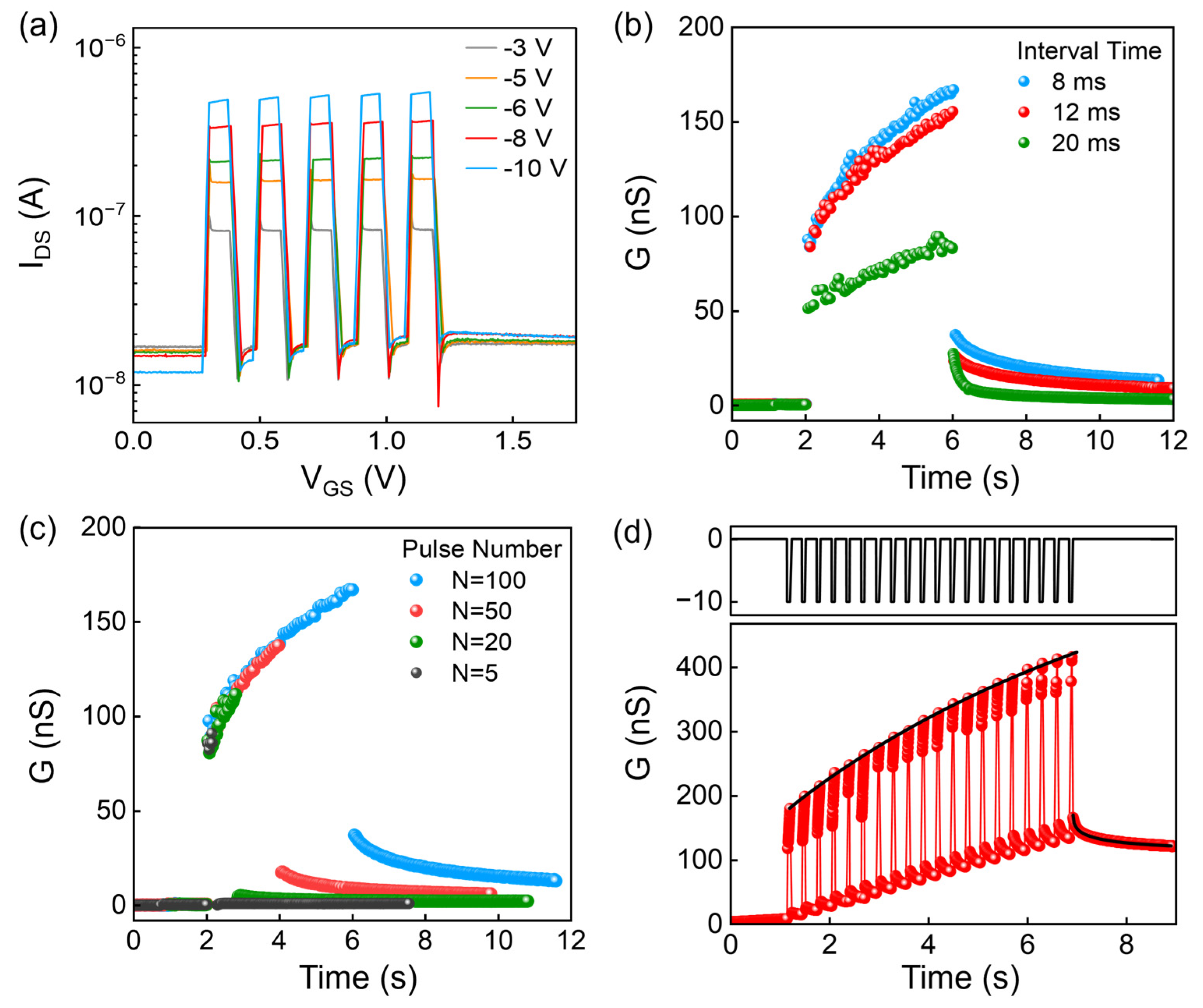
3.3. Synaptic Behavior

The variations in the polarization (P) of the ferroelectric domains can lead to the synaptic characteristics of OFe-FETs, which has provoked a significant interest in utilizing ferroelectric transistors as synaptic neurons. In general, by applying voltage pulses to the gate of OFe-FETs, the polarization of the ferroelectric films can be gradually altered, resulting in a consistent increase or decrease in the device current. This change strongly depends on the pulse voltage, pulse width, and the interval time between two pulses, reflecting the accumulation dynamics for the neuron implementation. To this end, we design various schemes of pulse inputs to the OFe-FETs by adjusting the pulse amplitude, number, and interval time.
Negative pulses with fixed pulse numbers (N = 5) and different amplitudes were first input (the amplitude of these pulses are −3 V, −5 V, −6 V, −8 V, and −10 V, respectively; see Figure 6a). The response current increases from 83 to 542 nA as the pulse amplitude increases from −3 to −10 V, confirming that higher pulse amplitude results in a wider variation of EPSC. This phenomenon can be explained by the model above. With the large input voltage, the Emax in Equations (1) and (2) increases and induces a more complete polarization switching (P), which leads to the enhanced conductance. Figure 6b shows the conductance response to pulse inputs with a fixed pulse number (N = 100) and different interval times (8, 12 and 20 ms). A shorter interval time resulted in the larger range of variation of the channel conductance (G). For example, G varies between 51 and 84 nS in response to the pulses with an interval time of 20 ms, and it varies between 83 and 167 nS in response to the pulses with an interval time of 8 ms. The high conductance state under pulse input with short interval time also resulted in a longer time to return to the initial state, which is similar to the forgetting process of brain memory. In terms of pulse number (N), pulses with a fixed amplitude (−4 V), a fixed interval time (12 ms) and different pulse number were input (the pulse number of these pulses are 5, 20, 50 and 100). Figure 6c shows that when the pulse number N is 5 (or 100), the conductance increased reaches 86 (or 167 nS) and returns to 1 nS (or 37 nS) immediately after the inputs. Based on these results, we applied a pulse sequence with an amplitude of −10 V (N = 20) to obtain the essential synaptic function: long-term potentiation (LTP) as shown in Figure 6d. The conductance maintains at 122 nS even after the pulse inputs are removed for a period of time.
By modulating the pulse amplitude, pulse number, and interval time, we were able to obtain the transition from STP to LTP, in which the fast/slow conductance decay is similar to the learning and forgetting processes of the brain [25]. The conductance update and decay with time G(t) can be fitted with two exponential functions: G p ( t ) = G p 0 1 e x p t t p n 1 + g 1 , G d ( t ) = G d 0 × e x p t t d n 2 + g 1 , where Gp and Gd are the conductance of potentiation and decay, respectively. Gp0, Gd0, g1, and g2 are parameters related to the initial polarization state. Parameters tp is the constant related to the ability to switch the polarization, while td is the decay constant. Furthermore, n1 and n2 are stretched exponents, which can be impacted by the pulse inputs. The experimental data can be well fitted as shown with solid lines in Figure 6d.

4. Conclusions

In conclusion, we have successfully fabricated the OFe-FETs which exhibited transfer characteristics with bias-sensitive and rate-dependent hysteresis windows. Quasi-static and dynamic characteristics are obtained by modulating the gate voltage sweeping. Moreover, we developed a compact analytical model for quasi-static transfer curves that delineates the electrical characteristics of OFe-FETs, by integrating the characteristic formula for ferroelectric polarization with a compact OFET model. The concordance between the model and a series of experimental data on transfer characteristics has been verified. These results have provided deeper insights into the behavior of OFe-FETs, particularly in regard to the modulation of subthreshold swing and the width of the hysteresis window by varying the sweeping rate of voltage sweeps. Synaptic plasticity-incorporating features such as excitatory postsynaptic current and both short-term and long-term potentiation is also demonstrated in our device. These results may allow a better understanding of OFe-FETs in memory applications, synthetic synapses, and other advanced electronic applications.

Author Contributions

Conceptualization, C.L. and H.K.; methodology, C.L. and H.K.; software, X.L.; validation, B.L. and C.L.; writing—original draft preparation, H.K.; investigation, H.K. and X.Y.; resources, B.L. and S.H.; writing—review and editing, C.L., X.S., S.H. and S.J.; funding acquisition, S.H. and C.L. All authors have read and agreed to the published version of the manuscript.

Funding

This work was supported by National Key Research and Development Program of China (No. 2022YFB3603901), and the National Natural Science Foundation of China (No. 62104262).

Data Availability Statement

The data that support the findings of this study are available within the article.

Conflicts of Interest

The authors declare no conflicts of interest.

References

  1. Yan, M.; Zhu, Q.; Wang, S.; Ren, Y.; Feng, G.; Liu, L.; Peng, H.; He, Y.; Wang, J.; Zhou, P.; et al. Ferroelectric Synaptic Transistor Network for Associative Memory. Adv. Electron. Mater. 2021, 7, 2001276. [Google Scholar] [CrossRef]
  2. Oh, S.; Kim, T.; Kwak, M.; Song, J.; Woo, J.; Jeon, S.; Yoo, I.K.; Hwang, H. HfZrOx-Based Ferroelectric Synapse Device With 32 Levels of Conductance States for Neuromorphic Applications. IEEE Electron Device Lett. 2017, 38, 732–735. [Google Scholar] [CrossRef]
  3. Sun, X.; Wang, P.; Ni, K.; Datta, S.; Yu, S. Exploiting Hybrid Precision for Training and Inference: A 2T-1FeFET Based Analog Synaptic Weight Cell. In Proceedings of the 2018 IEEE International Electron Devices Meeting (IEDM), San Francisco, CA, USA, 1–5 December 2018; pp. 3.1.1–3.1.4. [Google Scholar]
  4. Wang, H.; Yang, M.; Huang, Q.; Zhu, K.; Zhao, Y.; Liang, Z.; Chen, C.; Wang, Z.; Zhong, Y.; Zhang, X.; et al. New Insights into the Physical Origin of Negative Capacitance and Hysteresis in NCFETs. In Proceedings of the 2018 IEEE International Electron Devices Meeting (IEDM), San Francisco, CA, USA, 1–5 December 2018; pp. 31.31.31–31.31.34. [Google Scholar]
  5. Pahwa, G.; Dutta, T.; Agarwal, A.; Khandelwal, S.; Salahuddin, S.; Hu, C.; Chauhan, Y.S. Analysis and Compact Modeling of Negative Capacitance Transistor with High ON-Current and Negative Output Differential Resistance—Part II: Model Validation. IEEE Trans. Electron Devices 2016, 63, 4986–4992. [Google Scholar] [CrossRef]
  6. Aziz, A.; Ghosh, S.; Datta, S.; Gupta, S.K. Physics-Based Circuit-Compatible SPICE Model for Ferroelectric Transistors. IEEE Electron Device Lett. 2016, 37, 805–808. [Google Scholar] [CrossRef]
  7. Ni, K.; Jerry, M.; Smith, J.A.; Datta, S. A Circuit Compatible Accurate Compact Model for Ferroelectric-FETs. In Proceedings of the 2018 IEEE Symposium on VLSI Technology, Honolulu, HI, USA, 18–22 June 2018; pp. 131–132. [Google Scholar]
  8. Bae, I.; Kang, S.J.; Park, Y.J.; Furukawa, T.; Park, C. Organic ferroelectric field-effect transistor with P(VDF-TrFE)/PMMA blend thin films for non-volatile memory applications. Curr. Appl. Phys. 2010, 10, e54–e57. [Google Scholar] [CrossRef]
  9. Sun, H.; Wang, Q.; Li, Y.; Lin, Y.-F.; Wang, Y.; Yin, Y.; Xu, Y.; Liu, C.; Tsukagoshi, K.; Pan, L.; et al. Boost Up Carrier Mobility for Ferroelectric Organic Transistor Memory via Buffering Interfacial Polarization Fluctuation. Sci. Rep. 2014, 4, 7227. [Google Scholar] [CrossRef] [PubMed]
  10. Jung, S.-W.; Baeg, K.-J.; Yoon, S.-M.; You, I.-K.; Lee, J.-K.; Kim, Y.-S.; Noh, Y.-Y. Low-voltage-operated top-gate polymer thin-film transistors with high capacitance poly(vinylidene fluoride-trifluoroethylene)/poly(methyl methacrylate) dielectrics. J. Appl. Phys. 2010, 108, 102810. [Google Scholar] [CrossRef]
  11. Chang, J.; Shin, C.H.; Park, Y.J.; Kang, S.J.; Jeong, H.J.; Kim, K.J.; Hawker, C.J.; Russell, T.P.; Ryu, D.Y.; Park, C. Polymeric gate dielectric interlayer of cross-linkable poly(styrene-r-methylmethacrylate) copolymer for ferroelectric PVDF-TrFE field effect transistor memory. Org. Electron. 2009, 10, 849–856. [Google Scholar] [CrossRef]
  12. Hwang, S.K.; Bae, I.; Cho, S.M.; Kim, R.H.; Jung, H.J.; Park, C. High Performance Multi-Level Non-Volatile Polymer Memory with Solution-Blended Ferroelectric Polymer/High-k Insulators for Low Voltage Operation. Adv. Funct. Mater. 2013, 23, 5484–5493. [Google Scholar] [CrossRef]
  13. Song, L.; Wang, Y.; Gao, Q.; Guo, Y.; Wang, Q.; Qian, J.; Jiang, S.; Wu, B.; Wang, X.; Shi, Y.; et al. Speed up Ferroelectric Organic Transistor Memories by Using Two-Dimensional Molecular Crystalline Semiconductors. ACS Appl. Mater. Interfaces 2017, 9, 18127–18133. [Google Scholar] [CrossRef]
  14. Kim, C.H.; Bonnassieux, Y.; Horowitz, G. Compact DC Modeling of Organic Field-Effect Transistors: Review and Perspectives. IEEE Trans. Electron Devices 2014, 61, 278–287. [Google Scholar] [CrossRef]
  15. Chang Hyun, K.; Castro-Carranza, A.; Estrada, M.; Cerdeira, A.; Bonnassieux, Y.; Horowitz, G.; Iniguez, B. A Compact Model for Organic Field-Effect Transistors With Improved Output Asymptotic Behaviors. IEEE Trans. Electron Devices 2013, 60, 1136–1141. [Google Scholar] [CrossRef]
  16. Hang-Ting, L.; Chien-Jang, W.; Tseung-Yuen, T. Device modeling of ferroelectric memory field-effect transistor (FeMFET). IEEE Trans. Electron Devices 2002, 49, 1790–1798. [Google Scholar] [CrossRef]
  17. Miller, S.L.; McWhorter, P.J. Physics of the ferroelectric nonvolatile memory field effect transistor. J. Appl. Phys. 1992, 72, 5999–6010. [Google Scholar] [CrossRef]
  18. Cerdeira, A.; Estrada, M.; García, R.; Ortiz-Conde, A.; García Sánchez, F.J. New procedure for the extraction of basic a-Si:H TFT model parameters in the linear and saturation regions. Solid-State Electron. 2001, 45, 1077–1080. [Google Scholar] [CrossRef]
  19. Estrada, M.; Cerdeira, A.; Puigdollers, J.; Reséndiz, L.; Pallares, J.; Marsal, L.F.; Voz, C.; Iñiguez, B. Accurate modeling and parameter extraction method for organic TFTs. Solid-State Electron. 2005, 49, 1009–1016. [Google Scholar] [CrossRef]
  20. Brondijk, J.J.; Asadi, K.; Blom, P.W.M.; de Leeuw, D.M. Physics of organic ferroelectric field-effect transistors. J. Polym. Sci. Part B Polym. Phys. 2012, 50, 47–54. [Google Scholar] [CrossRef]
  21. Su, C.; Huang, Q.; Wang, K.; Fu, Z.; Huang, R. New Insights Into Memory Window of Ferroelectric FET Impacted by Read Operations With Awareness of Polarization Switching Dynamics. IEEE Trans. Electron Devices 2022, 69, 5310–5315. [Google Scholar] [CrossRef]
  22. Jin, C.; Saraya, T.; Hiramoto, T.; Kobayashi, M. On the Physical Mechanism of Transient Negative Capacitance Effect in Deep Subthreshold Region. IEEE J. Electron Devices Soc. 2019, 7, 368–374. [Google Scholar] [CrossRef]
  23. Sharma, P.; Zhang, J.; Ni, K.; Datta, S. Time-Resolved Measurement of Negative Capacitance. IEEE Electron Device Lett. 2018, 39, 272–275. [Google Scholar] [CrossRef]
  24. Tian, B.; Liu, L.; Yan, M.; Wang, J.; Zhao, Q.; Zhong, N.; Xiang, P.; Sun, L.; Peng, H.; Shen, H.; et al. A Robust Artificial Synapse Based on Organic Ferroelectric Polymer. Adv. Electron. Mater. 2019, 5, 1800600. [Google Scholar] [CrossRef]
  25. Li, Y.; Tao, R.; He, W.; Chang, C.; Zou, Z.; Zhang, Y.; Wang, D.; Wang, J.; Fan, Z.; Zhou, G.; et al. Realization of tunable artificial synapse through ambipolar charge trapping in organic transistor with pentacene/poly(α-methylstyrene) architecture. J. Appl. Phys. 2021, 129, 074903. [Google Scholar] [CrossRef]
Figure 1. (a) Schematic illustration of the OFe-FET structure. (b) Typical AFM image of spin-coated P(VDF-TrFE) thin film (scan size: 1 µm × 1 µm). (c) Schematic illustration of the MFM structure (the size of the square top electrodes: 200 µm × 200 µm). (d) Capacitance versus bias voltage result (swept from −12 to 12 V and then backward) for the MFM capacitor with an insulator layer of ~200 nm P(VDF-TrFE).
Micromachines 15 00467 g001
Figure 2. (a) Transfer characteristics measured at different VG sweeping ranges (VD = −1 V, the sweep direction has been denoted by arrows). (b) Schematic of the memory window when VG sweeps from 10 to −10 V and then backward.
Micromachines 15 00467 g002
Figure 3. (a) Framework of the compact OFe-FET model. (b) Equivalent circuit of OFe-FET.
Micromachines 15 00467 g003
Figure 4. (ad) Fitting results of quasi-static transfer curves at different VG sweeping ranges (symbols represent experimental data and red lines represent the calculated values, the sweep direction has been denoted by arrows).
Micromachines 15 00467 g004
Figure 5. (a) Transfer characteristic curves as a function of VG sweeping rate (inset: VG-t graph under various sweep rate and the definition of ts). (b) Corresponding memory window and (c) Smin as a function of ts (symbols represent experimental results and lines represent the fitting curves with fitting parameters a = 1.48, b = 1.3, c = −0.2, A = 4.5, B = 7.3, t0 = 0.16).
Micromachines 15 00467 g005
Figure 6. (a) Typical EPSC triggered by different pulse amplitude varying from −3 to −10 V. (b) Conductance response under varying pulse interval time. (c) Conductance response under varying pulse numbers. (d) LTP characteristics (−10 V, 60 ms; the red dots and red line represent the experimental data, while the balck solid lines are fitting with exponential functions Gp(t) and Gd(t)).
Micromachines 15 00467 g006
Disclaimer/Publisher’s Note: The statements, opinions and data contained in all publications are solely those of the individual author(s) and contributor(s) and not of MDPI and/or the editor(s). MDPI and/or the editor(s) disclaim responsibility for any injury to people or property resulting from any ideas, methods, instructions or products referred to in the content.

