
Analyzing Various Structural and Temperature Characteristics of Floating Gate Field Effect Transistors Applicable to Fine-Grain Logic-in-Memory Devices


Abstract
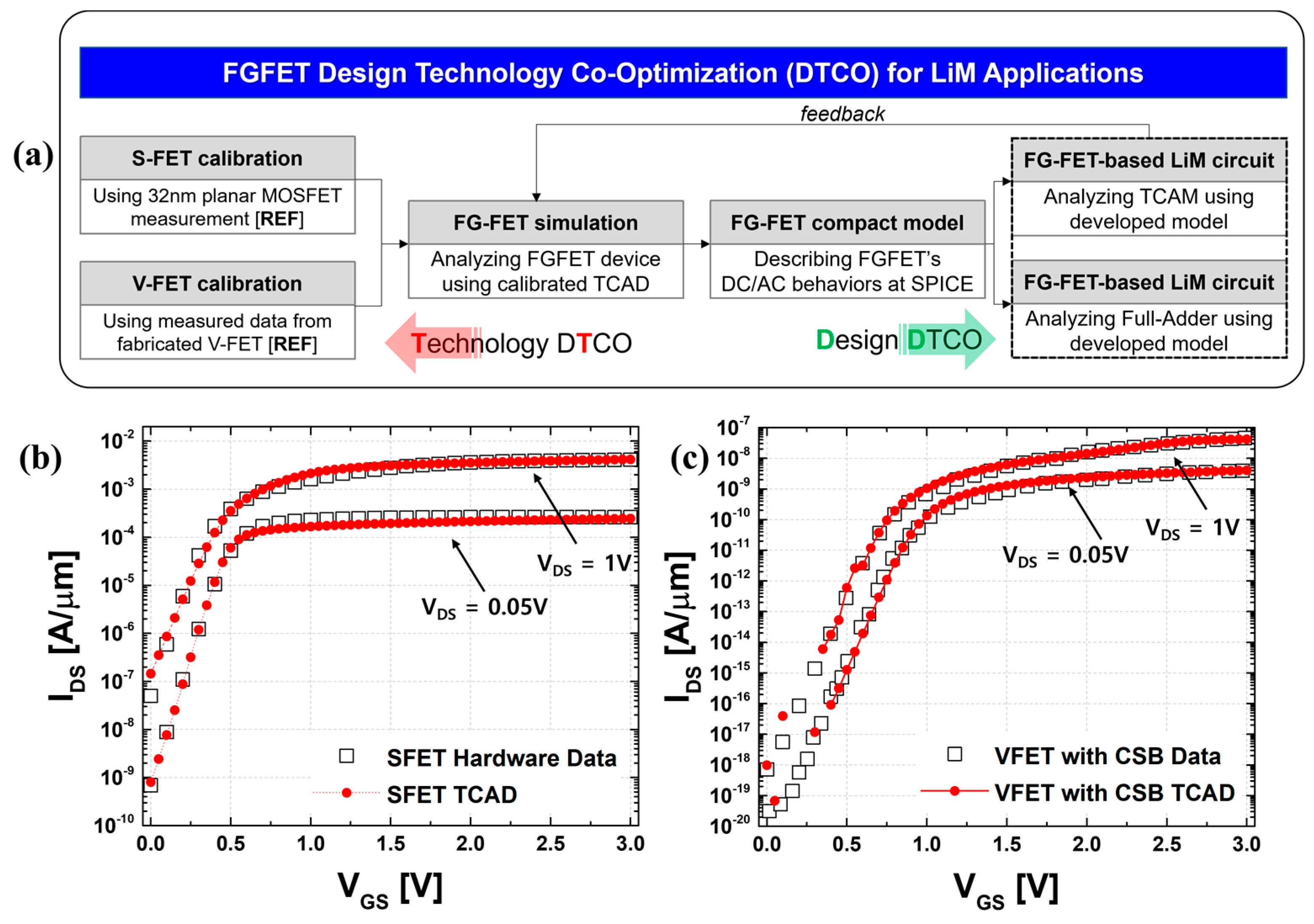
1. Introduction
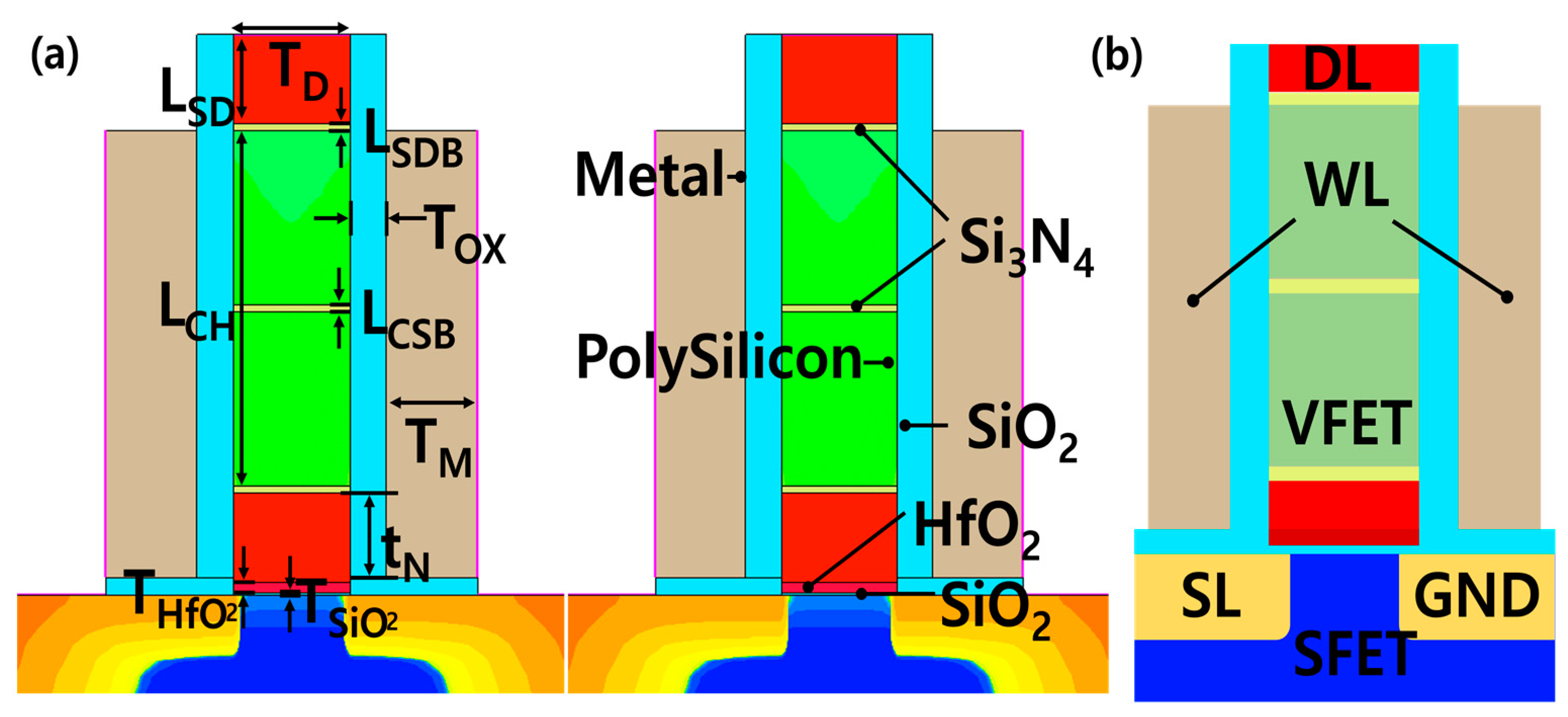
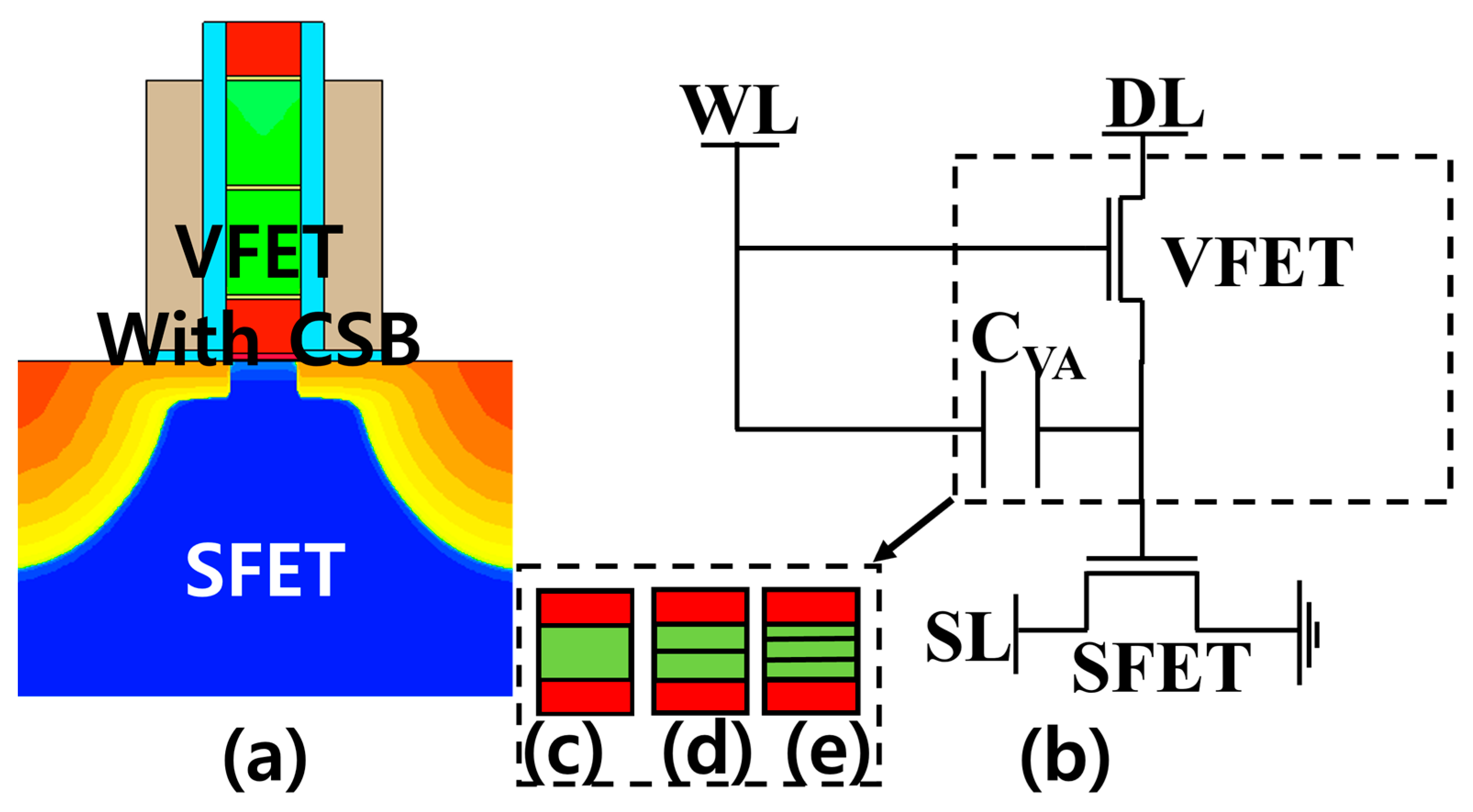
2. FGFET-SDB, -CSB Electrical Properties as a Function of Temperature
2.1. The Retention Time of FGFET-CSB and SDB
2.2. The Memory Window of FGFET-CSB and SDB
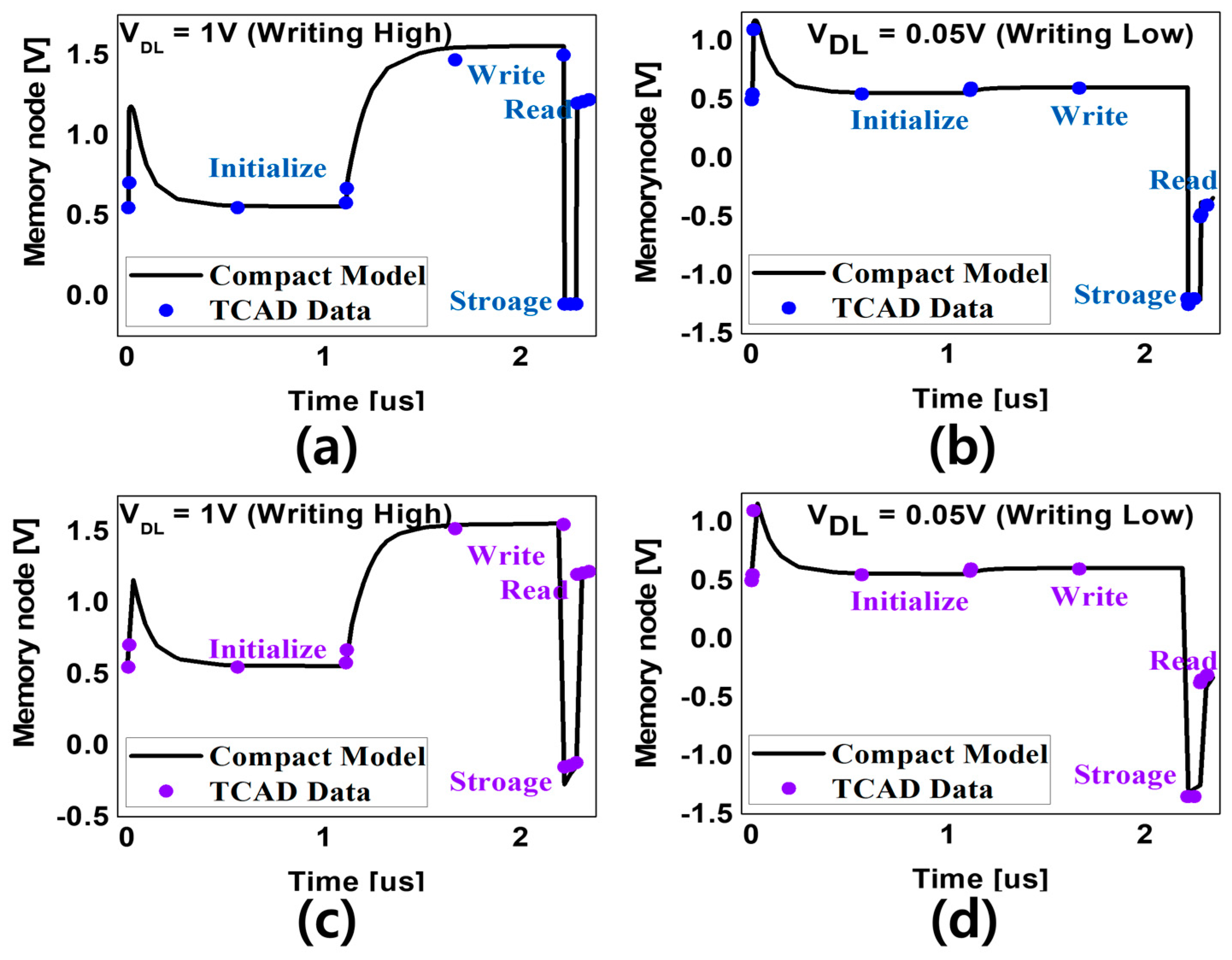
3. FGFET Compact Modeling and Circuit Characterization for LiM Applicability
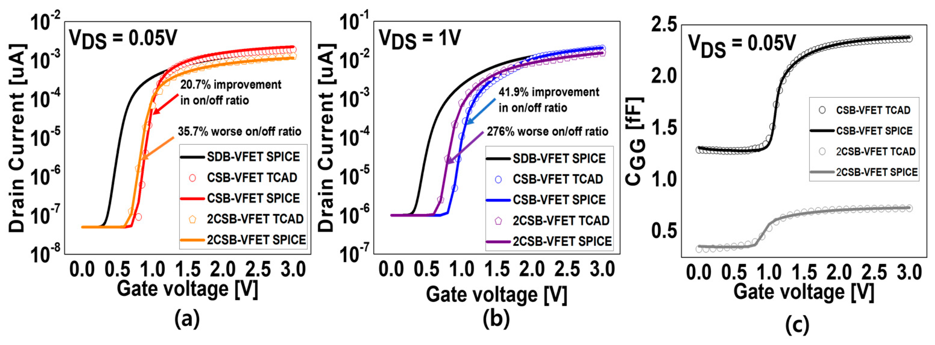
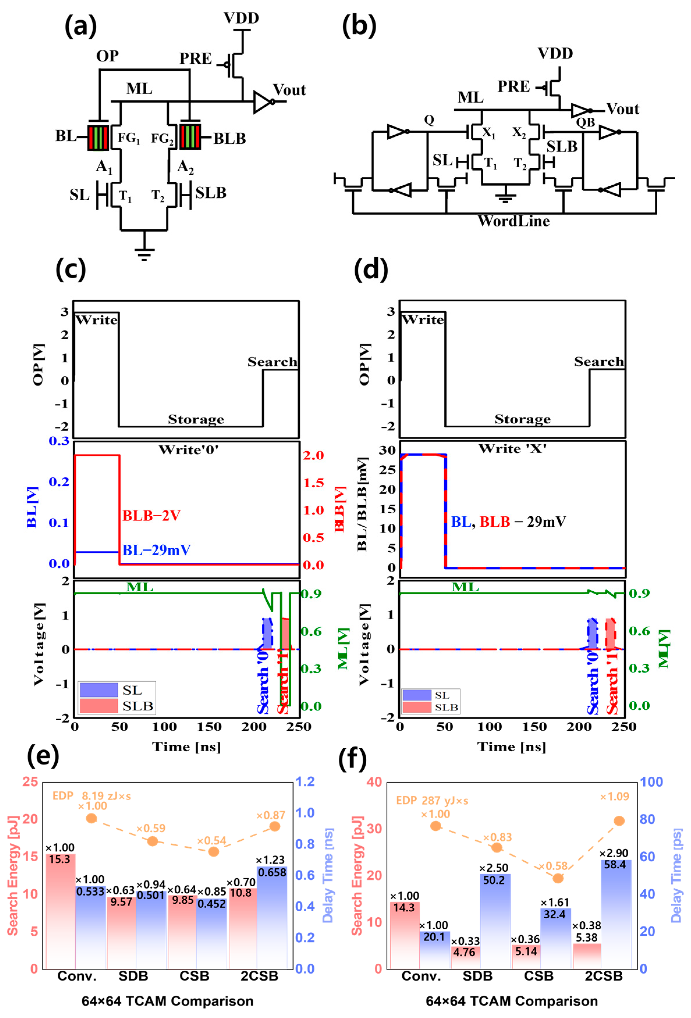
3.1. TCAM, FA Circuit Characteristics with and without Central Shallow Barriers
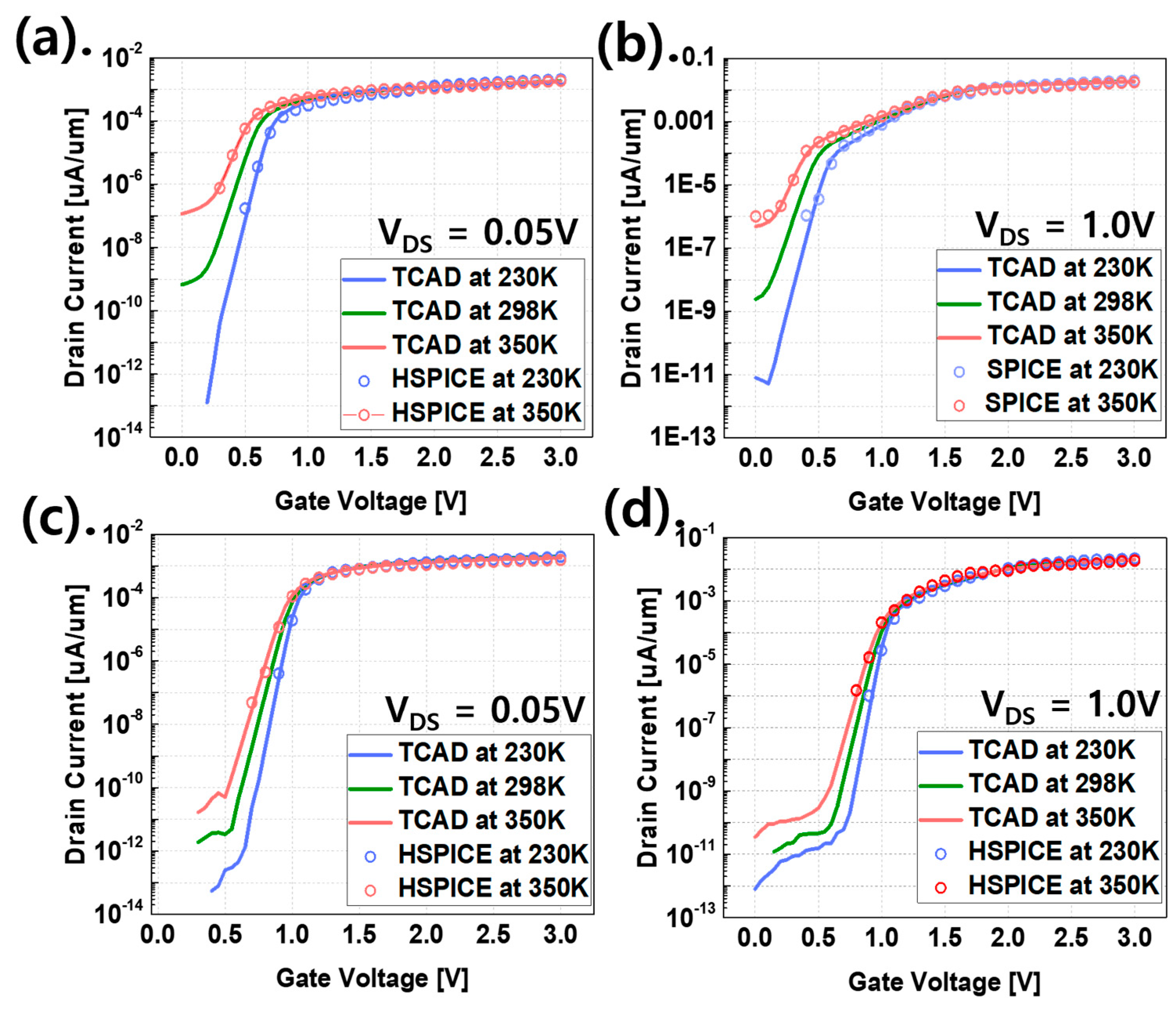
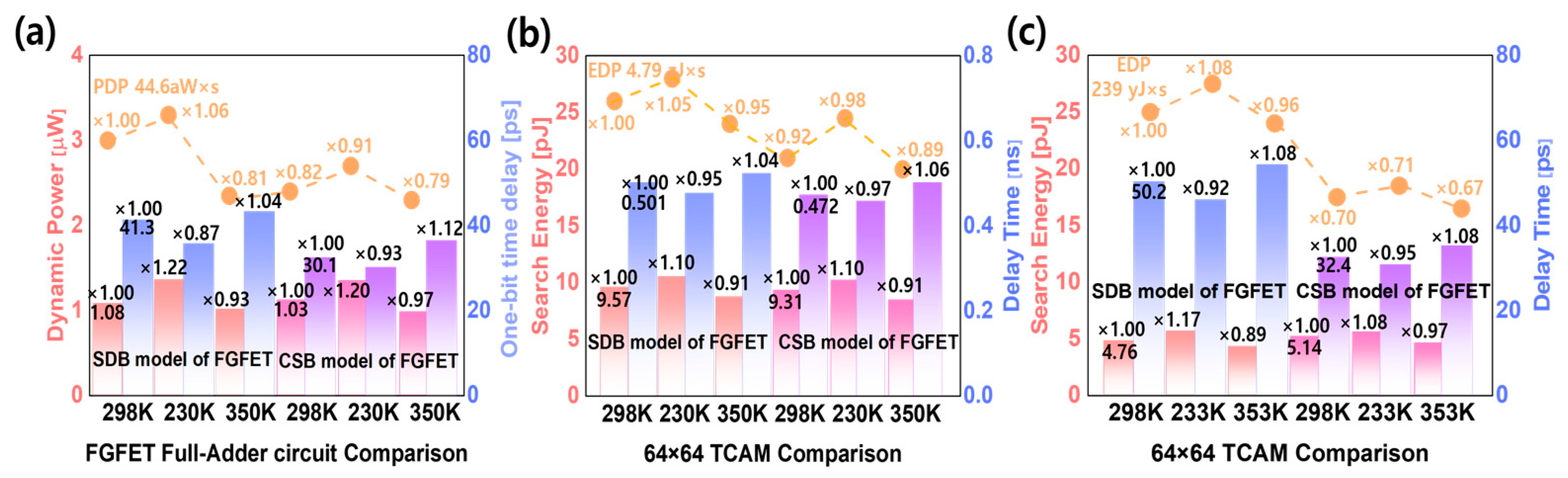
3.2. TCAM, FA Circuit Characteristics of FGFET Devices by Temperature
4. Neural Network Availability for FGFET Devices
5. Conclusions
Author Contributions
Funding
Data Availability Statement
Acknowledgments
Conflicts of Interest
References
- Wulf, W.A.; McKee, S.A. Hitting the memory wall: Implications of the obvious. ACM SIGARCH Comput. Archit. News 1995, 23, 20–24. [Google Scholar] [CrossRef]
- Sebastian, A.; Le Gallo, M.; Khaddam-Aljameh, R.; Eleftheriou, E. Memory devices and applications for in-memory computing. Nat. Nanotechnol. 2020, 15, 529–544. [Google Scholar] [CrossRef]
- Verma, N.; Jia, H.; Valavi, H.; Tang, Y.; Ozatay, M.; Chen, L.Y.; Zhang, B.; Deaville, P. In-memory computing: Advances and prospects. IEEE Solid-State Circuits Mag. 2019, 11, 43–55. [Google Scholar] [CrossRef]
- Chen, B.; Cai, F.; Zhou, J.; Ma, W.; Sheridan, P.; Lu, W.D. Efficient in-memory computing architecture based on crossbar arrays. In Proceedings of the 2015 IEEE International Electron Devices Meeting (IEDM), Washington, DC, USA, 7–9 December 2015; pp. 17.5.1–17.5.4. [Google Scholar]
- Karunaratne, G.; Le Gallo, M.; Cherubini, G.; Benini, L.; Rahimi, A.; Sebastian, A. In-memory hyperdimensional computing. Nat. Electron. 2020, 3, 327–337. [Google Scholar] [CrossRef]
- Papandroulidakis, G.; Vourkas, I.; Abusleme, A.; Sirakoulis, G.C.; Rubio, A. Crossbar-based memristive logic-in-memory architecture. IEEE Trans. Nanotechnol. 2017, 16, 491–501. [Google Scholar] [CrossRef]
- Ielmini, D.; Wong, H.S.P. In-memory computing with resistive switching devices. Nat. Electron. 2018, 1, 333–343. [Google Scholar] [CrossRef]
- Yin, X.; Chen, X.; Niemier, M.; Hu, X.S. Ferroelectric FETs-based nonvolatile logic-in-memory circuits. IEEE Trans. Very Large Scale Integr. (VLSI) Syst. 2018, 27, 159–172. [Google Scholar] [CrossRef]
- O’Connor, I.; Cantan, M.; Marchand, C.; Vilquin, B.; Slesazeck, S.; Breyer, E.T.; Mulaosmanovic, H.; Mikolajick, T.; Giraud, B.; Noël, J.-P.; et al. Prospects for energy-efficient edge computing with integrated HfO 2-based ferroelectric devices. In Proceedings of the 2018 IFIP/IEEE International Conference on Very Large Scale Integration (VLSI-SoC), Verona, Italy, 8–10 October 2018; pp. 180–183. [Google Scholar]
- Ni, K.; Yin, X.; Laguna, A.F.; Joshi, S.; Dünkel, S.; Trentzsch, M.; Müller, J.; Beyer, S.; Niemier, M.; Hu, X.S.; et al. Ferroelectric ternary content-addressable memory for one-shot learning. Nat. Electron. 2019, 2, 521–529. [Google Scholar] [CrossRef]
- Mizuta, H.; Wagner, M.; Nakazato, K. The role of tunnel barriers in phase-state low electron-number drive transistors (PLEDTRs). IEEE Trans. Electron Devices 2001, 48, 1103–1108. [Google Scholar] [CrossRef]
- Kim, K.D.; Lee, K.H.; Baik, S.J.; Lee, J.H.; Kim, T.K.; Kong, J.T. Characterization of multi-barrier tunneling diodes and vertical transistors using 2-D device simulation. In Proceedings of the International Conference on Simulation of Semiconductor Processes and Devices, Kobe, Japan, 4–6 September 2002; pp. 167–170. [Google Scholar]
- Ahn, S.J.; Koh, G.H.; Kwon, K.W.; Baik, S.J.; Jung, G.T.; Hwang, Y.N.; Jeong, H.S.; Kim, K. Highly scalable and CMOS-compatible STTM cell technology. In Proceedings of the IEEE International Electron Devices Meeting 2003, Washington, DC, USA, 8–10 December 2003; pp. 10.4.1–10.4.4. [Google Scholar]
- Baik, S.J.; Huo, Z.; Lim, S.H.; Yeo, I.S.; Choi, S.; Chung, U.I.; Moon, J.T. STTM-promising nanoelectronic DRAM device. In Proceedings of the 4th IEEE Conference on Nanotechnology, 2004, Munich, Germany, 16–19 August 2004; pp. 45–46. [Google Scholar]
- Nakazato, K.; Itoh, K.; Ahmed, H.; Mizuta, H.; Kisu, T.; Kato, M.; Sakata, T. Phase-state low electron-number drive random access memory (PLEDM). In Proceedings of the 2000 IEEE International Solid-State Circuits Conference. Digest of Technical Papers (Cat. No. 00CH37056), San Francisco, CA, USA, 9 February 2000; pp. 132–133. [Google Scholar]
- Kang, S.; Cho, W.Y.; Choi, B.G.; Cho, B.; Oh, H.R.; Kim, H.J.; Baik, S.-J.; Kim, D.; Kwak, C.-K.; Byun, H.-G. Scalable Two Transistor Memory (STTM) for mobile embedded applications with 80nm technology. In Proceedings of the International SoC Design Conference (ISOCC), Seoul, Korea, 26–27 October 2004; pp. 159–162. [Google Scholar]
- Beyer, S.; Dünkel, S.; Trentzsch, M.; Müller, J.; Hellmich, A.; Utess, D.; Paul, J.; Pellerin, J.; Müller, S.; Ocker, J. FeFET: A versatile CMOS compatible device with game-changing potential. In Proceedings of the 2020 IEEE International Memory Workshop (IMW), Dresden, German, 17–20 May 2020; pp. 1–4. [Google Scholar]
- Huang, P.; Han, R.; Kang, J. AI learns how to learn with TCAMs. Nat. Electron. 2019, 2, 493–494. [Google Scholar] [CrossRef]
- Khan, A.I.; Keshavarzi, A.; Datta, S. The future of ferroelectric field-effect transistor technology. Nat. Electron. 2020, 3, 588–597. [Google Scholar] [CrossRef]
- Li, X.; Ma, K.; George, S.; Khwa, W.S.; Sampson, J.; Gupta, S.; Liu, Y.; Chang, M.-F.; Datta, S.; Narayanan, V. Design of nonvolatile SRAM with ferroelectric FETs for energy-efficient backup and restore. IEEE Trans. Electron Devices 2017, 64, 3037–3040. [Google Scholar] [CrossRef]
- Cho, S.; Kim, S.; Choi, I.; Kang, M.; Baik, S.; Jeon, J. Non-volatile logic-in-memory ternary content addressable memory circuit with floating gate field effect transistor. AIP Adv. 2023, 13, 045211. [Google Scholar] [CrossRef]
- Kim, S.; Choi, I.; Cho, S.; Kang, M.; Baik, S.; Ra, C.; Jeon, J. Analysis of Logic-in-Memory Full Adder Circuit with Floating Gate Field Effect Transistor (FGFET). IEEE Access 2023, 11, 97778–97785. [Google Scholar] [CrossRef]
- Kim, S.; Cho, S.; Choi, I.; Kang, M.; Baik, S.; Jeon, J. Investigation on floating-gate field-effect transistor for logic-in-memory application. J. Phys. D Appl. Phys. 2023, 56, 495105. [Google Scholar] [CrossRef]
- Kim, Y.; Kim, H.; Jeon, J.; Baik, S.; Kang, M. Circuit simulation of floating-gate FET (FGFET) for logic application. Mem.-Mater. Devices Circuits Syst. 2023, 6, 100090. [Google Scholar] [CrossRef]
- Sentaurus Device User Guide, Version P-2019.03 2019 (Synopsys TCAD Sentaurus). Available online: https://picture.iczhiku.com/resource/eetop/WHItQPrSdRjDtBnb.pdf (accessed on 28 September 2023).
- ITRS 2005 The International Technology Road Map for Semiconductors. Available online: https://www.semiconductors.org/resources/2005-international-technology-roadmap-for-semiconductors-itrs/ (accessed on 28 September 2023).
- Zhao, W.; Cao, Y. Predictive technology model for nano-CMOS design exploration. ACM J. Emerg. Technol. Comput. Syst. (JETC) 2007, 3, 1-es. [Google Scholar] [CrossRef]
- Allan, A. ITRS roadmap. In Proceedings of the 2007 ITRS Conference, Shanghai, China, 21 September 2007. [Google Scholar]
- Kuhn, K.J. Moore’s Law Past 32nm: Future Challenges in Device Scaling. In Proceedings of the 2009 13th International Workshop on Computational Electronics, Beijing, China, 27–29 May 2009; pp. 1–6. [Google Scholar]
- PTM SPICE MODELS DOWNLOADS—Sub Micron nm CMOS Models. Available online: http://www.elecdude.com/2013/05/ptm-spice-models-downloads-sub-micron.html (accessed on 6 May 2013).
- Cao, Y.; Sato, T.; Orshansky, M.; Sylvester, D.; Hu, C. New paradigm of predictive MOSFET and interconnect modeling for early circuit simulation. In Proceedings of the IEEE 2000 Custom Integrated Circuits Conference (Cat. No. 00CH37044), Orlando, FL, USA, 24 May 2000; pp. 201–204. [Google Scholar]
- Zanotti, T.; Puglisi, F.M.; Pavan, P. Smart logic-in-memory architecture for low-power non-von neumann computing. IEEE J. Electron Devices Soc. 2020, 8, 757–764. [Google Scholar] [CrossRef]
- Yin, X.; Aziz, A.; Nahas, J.; Datta, S.; Gupta, S.; Niemier, M.; Hu, X.S. Exploiting ferroelectric FETs for low-power non-volatile logic-in-memory circuits. In Proceedings of the 2016 IEEE/ACM International Conference on Computer-Aided Design (ICCAD), Austin, TX, USA, 7–10 November 2016; pp. 1–8. [Google Scholar]
- Breyer, E.T.; Mulaosmanovic, H.; Trommer, J.; Melde, T.; Dünkel, S.; Trentzsch, M.; Beyer, S.; Slesazeck, S.; Mikolajick, T. Compact FeFET circuit building blocks for fast and efficient nonvolatile logic-in-memory. IEEE J. Electron Devices Soc. 2020, 8, 748–756. [Google Scholar] [CrossRef]
- Guo, Q.; Guo, X.; Bai, Y.; Ipek, E. A resistive TCAM accelerator for data-intensive computing. In Proceedings of the 44th Annual IEEE/ACM International Symposium on Microarchitecture, Porto Alegre, Brazil, 3–7 December 2011; pp. 339–350. [Google Scholar]
- Imani, M.; Patil, S.; Rosing, T.S. MASC: Ultra-low energy multiple-access single-charge TCAM for approximate computing. In Proceedings of the 2016 Design, Automation & Test in Europe Conference & Exhibition (DATE), Dresden, Germany, 14–18 March 2016; pp. 373–378. [Google Scholar]
- Garzón, E.; Lanuzza, M.; Teman, A.; Yavits, L. AM4: MRAM crossbar based CAM/TCAM/ACAM/AP for in-memory computing. IEEE J. Emerg. Sel. Top. Circuits Syst. 2023, 13, 408–421. [Google Scholar] [CrossRef]
- Mead, C. Neuromorphic electronic systems. Proc. IEEE 1990, 78, 1629–1636. [Google Scholar] [CrossRef]
- Woo, J.; Moon, K.; Song, J.; Lee, S.; Kwak, M.; Park, J.; Hwang, H. Improved synaptic behavior under identical pulses using AlOx/HfO2 bilayer RRAM array for neuromorphic systems. IEEE Electron Device Lett. 2016, 37, 994–997. [Google Scholar] [CrossRef]
- Gao, L.; Wang, I.T.; Chen, P.Y.; Vrudhula, S.; Seo, J.S.; Cao, Y.; Hou, T.-H.; Yu, S. Fully parallel write/read in resistive synaptic array for accelerating on-chip learning. Nanotechnology 2015, 26, 455204. [Google Scholar] [CrossRef]
- Park, S.; Sheri, A.; Kim, J.; Noh, J.; Jang, J.; Jeon, M.; Lee, B.; Lee, B.R.; Lee, B.H.; Huang, H. Neuromorphic speech systems using advanced ReRAM-based synapse. In Proceedings of the 2013 IEEE International Electron Devices Meeting, Washington, DC, USA, 9–11 December 2013; pp. 25.6.1–25.6.4. [Google Scholar]
- Tang, J.; He, C.; Tang, J.; Yue, K.; Zhang, Q.; Liu, Y.; Wang, Q.; Wang, S.; Li, N.; Shen, C.; et al. A reliable all-2D materials artificial synapse for high energy-efficient neuromorphic computing. Adv. Funct. Mater. 2021, 31, 2011083. [Google Scholar] [CrossRef]


| Parameters | Values |
|---|---|
| Gate separation (TD) | 32 nm |
| VFET gate oxide thickness (Tox) | 10 nm |
| Metal thickness (TM) | 25 nm |
| VFET channel length (LCH) | 100.2 nm |
| Source/drain length (LSD) | 25 nm |
| Source/drain barrier (LSDB) | 2 nm |
| Central shallow barrier (LCSB) | 2 nm |
| VFET channel doping | Intrinsic |
| VFET S/D doping | 2 × 1020 cm−3 |
| Memory node thickness (tN) | 23.7 nm |
| SiO2 thickness (TSiO2) | 0.7 nm |
| HfO2 thickness (THfO2) | 3 nm |
| Substrate doping | 1.0 × 10¹⁶~1.8 × 1016 cm−3 |
| SFET source/drain doping | 5 × 1019 cm−3 |
| Mode | VWL [V] | VDL [V] | VSL [V] |
|---|---|---|---|
| Initialize | 3 | 0 | 0 |
| Write | 3 | 0.05 (low, Data ‘0’)/1 (high, Data ‘1’) | 0 |
| Storage | −2 | 0 | 0 |
| Read | 0.5 | 0 | 0.9 |
| SDB Model | CSB Model | |||||
|---|---|---|---|---|---|---|
| TEM | 230 K | 298 K | 350 K | 230 K | 298 K | 350 K |
| MW [V] | 1.16 | 1.14 | 1.12 | 1.24 | 1.22 | 1.21 |
| Increase/decrease Rate [%] | 1.75 | 0 | −1.75 | 8.77 | 7.02 | 6.14 |
Disclaimer/Publisher’s Note: The statements, opinions and data contained in all publications are solely those of the individual author(s) and contributor(s) and not of MDPI and/or the editor(s). MDPI and/or the editor(s) disclaim responsibility for any injury to people or property resulting from any ideas, methods, instructions or products referred to in the content. |
© 2024 by the authors. Licensee MDPI, Basel, Switzerland. This article is an open access article distributed under the terms and conditions of the Creative Commons Attribution (CC BY) license (https://creativecommons.org/licenses/by/4.0/).
Share and Cite
Cho, S.; Kim, S.; Kang, M.; Baik, S.; Jeon, J. Analyzing Various Structural and Temperature Characteristics of Floating Gate Field Effect Transistors Applicable to Fine-Grain Logic-in-Memory Devices. Micromachines 2024, 15, 450. https://doi.org/10.3390/mi15040450
Cho S, Kim S, Kang M, Baik S, Jeon J. Analyzing Various Structural and Temperature Characteristics of Floating Gate Field Effect Transistors Applicable to Fine-Grain Logic-in-Memory Devices. Micromachines. 2024; 15(4):450. https://doi.org/10.3390/mi15040450
Chicago/Turabian StyleCho, Sangki, Sueyeon Kim, Myounggon Kang, Seungjae Baik, and Jongwook Jeon. 2024. "Analyzing Various Structural and Temperature Characteristics of Floating Gate Field Effect Transistors Applicable to Fine-Grain Logic-in-Memory Devices" Micromachines 15, no. 4: 450. https://doi.org/10.3390/mi15040450
APA StyleCho, S., Kim, S., Kang, M., Baik, S., & Jeon, J. (2024). Analyzing Various Structural and Temperature Characteristics of Floating Gate Field Effect Transistors Applicable to Fine-Grain Logic-in-Memory Devices. Micromachines, 15(4), 450. https://doi.org/10.3390/mi15040450