Abstract
Gallium oxide (Ga2O3) devices have shown remarkable potential for high-voltage, high-power, and low-loss power applications. However, thermal management of packaging for Ga2O3 devices becomes challenging due to the significant self-heating effect. In this paper, an advanced double-sided cooling flip-chip packaging structure for Ga2O3 devices was proposed and the overall packaging of Ga2O3 chips was researched by simulation in detail. The advanced double-sided cooling flip-chip packaging structure was formed by adding a layer of diamond material on top of the device based on the single-sided flip-chip structure. With a power density of 3.2 W/mm, it was observed that the maximum temperature of the Ga2O3 chip with the advanced double-sided cooling flip-chip packaging structure was 103 °C. Compared with traditional wire bonding packaging and single-sided cooling flip-chip packaging, the maximum temperature was reduced by about 12 °C and 7 °C, respectively. When the maximum temperature of the chip was controlled at 200 °C, the Ga2O3 chip with double-sided cooling packaging could reach a power density of 6.8 W/mm. Finally, by equipping the top of the package with additional water-cooling equipment, the maximum temperature was reduced to 186 °C. These findings highlight the effectiveness of the proposed flip-chip design with double-sided cooling in enhancing the heat dissipation capability of Ga2O3 chips, suggesting promising prospects for this advanced packaging structure.
1. Introduction
Third-generation semiconductor materials, with high breakdown voltage, electron mobility, thermal stability, and radiation resistance, are increasingly employed in the field of high-frequency, high-power, and high-integration electronic devices [1,2,3]. After years of development, power devices based on third-generation wide-band-gap semiconductor materials have gradually approached or even surpassed the performance of silicon-based semiconductor power devices [4,5]. Gallium oxide (Ga2O3), a new type of third-generation semiconductor material, has a larger band gap, higher breakdown field strength, and larger Baliga figure of merit. Compared with other commonly used third-generation wide-band-gap semiconductor materials such as GaN and SiC, Ga2O3 presents great potential for future applications in the fields of high-voltage, high-power, low-loss power devices due to its lower production cost [6,7,8,9].
However, the thermal conductivity of Ga2O3 is only 10–27 W/m K at room temperature. The low thermal conductivity prevents the heat inside the Ga2O3 devices from dissipating out rapidly, and the heat will accumulate, leading to the increase of the internal temperature of the device. The serious self-heating effect will limit the further improvement of the device power density and will even cause reliability problems of the device and reduce the operation life of the device [10,11,12]. Some studies have been reported to relieve the self-heating effect of Ga2O3 devices by optimizing the device structure and the process design. S. H. Kim et al. investigated the effects of anisotropic thermal conductivity of β-Ga2O3 and the geometric design of metal electrode interconnections on device self-heating [13], demonstrating the importance of device layout design of transverse β-Ga2O3 transistors to maximize the electrical and thermal properties. R. H. Montgomery et al. proposed the use of thermally conductive dielectrics on β-Ga2O3 MOSFETs with a vertical channel structure to increase the device power density [14]. B. Chatterjee et al. performed a thermal analysis of multi-fin Ga2O3 vertical transistors using infrared thermal microscopy and coupled electro-thermal modeling to investigate the self-heating behavior of Fin-FETs with different numbers of fins, fin design parameters, and device orientation to further reduce the thermal resistance [15].
In practical applications, in addition to researching the device itself to suppress the self-heating effect, more improvements were carried out in the thermal design of the chip package [16,17,18]. B. Chatterjee and K. Zeng et al. developed a three-dimensional coupled electro-thermal model based on the electro-thermal characterization results and tested the effectiveness of various active and passive cooling solutions [16]. C. Yuan et al. explored the limitations of various core-level thermal management schemes on Ga2O3 MOSFETs using numerical simulations and comprehensively investigated the effects of various cooling methods and material choices on the device channel temperature [17]. S. Kim et al. conducted a thermal modeling study on Ga2O3 vertical transistors and analyzed the effects of thermal management strategies on their thermal performances [18].
Based on the above-mentioned research, this paper further explored the thermal behaviors of Ga2O3 chip packaged by a Ga2O3 device, proposed an enhanced double-sided cooling flip-chip packaging structure based on diamond material, carried out the design of package structure and package thermal materials, and conducted a detailed study on the thermal performance of the overall package of this enhanced Ga2O3 chip through simulation. Compared with the traditional wire bonding packaging and single-sided cooling flip-chip packaging, it can be seen that the double-sided cooling flip-chip packaging structure proposed in this paper has a better effect on the heat dissipation of Ga2O3 chips and has a good application prospect.
2. Modeling of Wire Bonding and Single-Sided Cooling Flip-Chip Packaging
In the design of the package, this paper refers to the Ga2O3 device, which had been reported in Ref. [3]. The bottom substrate of the device is Si of 0.15 mm, and the maximum drain current density (IDS) is 80 mA/mm at the VDS of 40 V, which means the power density is 3.2 W/mm (LDS = 20 μm). The device model structure is shown in Figure 1. In the simulation, the heat source was added at the channel of the active layer below the gate, the size of the heat source was set to 200 μm × 5 μm × 0.2 μm, and the heat dissipation rate was set to 64 mW.
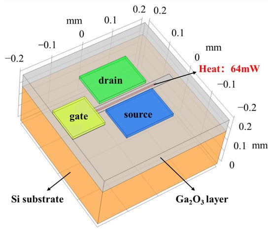
Figure 1.
Ga2O3 device model.
The structures of the wire bonding and single-sided cooling flip-chip models are shown in Figure 2a,b, respectively. The substrate of both the wire bonding and single-sided cooling flip-chip models was made of Al2O3 ceramic material, and a layer of Cu as an additional high thermal conductivity material was attached to the bottom of the substrate by solder. The outer package was made of epoxy molding plastic. Wire bonding was carried out with copper wire with a diameter of 20 μm. The device of the flip-chip packaging model was inverted on the substrate and electrically interconnected with the substrate through copper pillars with a radius of 20 μm and a height of 99 μm; then the device was fixed and protected with epoxy resin bottom-filling adhesive with 70% silica content. Detailed information on the size and material parameters of the package design is listed in Table 1.

Figure 2.
Simulated packaging model: (a) Wire bonding model; (b) single-sided cooling flip-chip model.

Table 1.
Size and Material Parameters of Wire Bonding and Flip-chip Packaging.
The temperature distribution of the wire bonding packaging is shown in Figure 3a. The maximum temperature of the wire bonding packaging was 115 °C. The temperature distribution of the single-sided cooling flip-chip packaging is shown in Figure 3b. The maximum temperature of the flip-chip packaging was 110 °C, which was 5 °C lower than that of the wire bonding packaging. Therefore, the flip-chip packaging could improve the heat dissipation of the Ga2O3 chip effectively compared with the wire bonding packaging. This is because, in the flip-chip packaging, the heat generated by the chip can be directly transferred to the substrate through the interconnecting copper pillars, and then the heat is transferred to the bottom high thermal conductivity Cu layer.
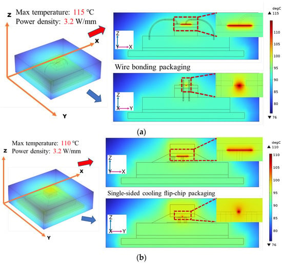
Figure 3.
Thermal simulation results of wire bonding packaging and single-sided cooling flip-chip packaging. (a) Wire bonding packaging; (b) single-sided cooling flip-chip packaging.
3. Double-Sided Cooling Flip-Chip Packaging
This paper proposes an advanced double-sided cooling flip-chip packaging structure for Ga2O3 devices. Based on the above single-sided flip-chip structure, a layer of high thermal conductivity material was added on top of the device to form a double-sided cooling heat dissipation structure, so that the heat of the device could be dissipated from the device down through the alumina ceramic and the Cu base plate on the bottom side and up through the Si substrate and high thermal conductivity material on the top side. The high thermal conductivity material above the device was diamond material with excellent thermal conductivity up to 2500 W/m·K, and the size of the diamond was 2 × 2 × 0.1 mm3. The advanced double-sided cooling flip-chip packaging model and the heat dissipation path are shown in Figure 4.

Figure 4.
Schematic of the double-sided cooling flip-chip packaging model and heat dissipation path. (a) Double-sided cooling flip-chip packaging model; (b) schematic of the double-sided cooling heat dissipation path.
The thermal simulation result of the enhanced double-sided cooling flip-chip Ga2O3 chip is shown in Figure 5. The maximum temperature was at the active layer of the device, and it can be observed that heat is transferred both upwards and downwards simultaneously. The maximum temperature of the double-sided cooling flip-chip package was 103 °C; compared with the traditional wire bonding package in Figure 3a and the single-sided cooling flip-chip packaging in Figure 3b, the maximum temperature was reduced by about 12 °C and 7 °C, respectively. The simulation results of maximum temperature are shown in Table 2.
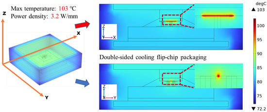
Figure 5.
Thermal simulation result of enhanced double-sided cooling flip-chip Ga2O3 chip.

Table 2.
Maximum Temperature Simulation Results of Different Packaging Models.
By changing the size of the heat source, the simulation results showed that the maximum power density was 6.8 W/mm at the maximum temperature of 200 °C for the enhanced double-sided cooling flip-chip Ga2O3 chip (Figure 6). To further improve the heat dissipation of the chip, additional cooling equipment is often added on top of the package, such as air-cooling or water-cooling equipment. This paper assumed that water-cooling equipment on the top of the double-sided cooling flip-chip Ga2O3 chip could keep the top of the package at 150 °C, and the situation of heat dissipation with water-cooling equipment was simulated by adding boundary temperature conditions (Figure 7). The simulation result is shown in Figure 8. The maximum temperature of the chip was 186 °C with a power density of 6.8 W/mm, which was effectively reduced by 14 °C. Therefore, the double-sided cooling flip-chip packaging structure combined with external cooling equipment will be a feasible and practical solution to the thermal management challenges of high-power Ga2O3 devices.
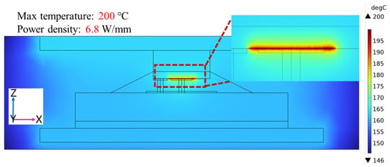
Figure 6.
Simulation results of double-sided cooling flip-chip packaging model at a power density of 6.8 W/mm.

Figure 7.
Schematic of the double-sided cooling flip-chip packaging model with water-cooling equipment.
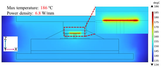
Figure 8.
Simulation result of double-sided cooling flip-chip packaging Ga2O3 chip model with water-cooling equipment at a power density of 6.8 W/mm.
4. Conclusions
Different Ga2O3 device packaging structures were simulated and studied in this paper. It was found that the maximum temperature of the single-sided flip-chip packaging was 5 °C lower than that of the wire-bonding packaging at a power density of 3.2 W/mm. In addition, an advanced double-sided cooling flip-chip packaging structure for Ga2O3 chips was proposed in this paper. The heat of the die could be dissipated from the die downward through the alumina ceramic and Cu base plate and could also be dissipated from the die upward through the diamond material. The simulation results showed that the maximum temperature of the chip with a double-sided cooling flip-chip structure was 7 °C lower than that of the single-sided cooling flip-chip structure and 12 °C lower than that of the traditional wire bonding packaging, which effectively reduced the temperature of the chip. In addition, the maximum power density of 6.8 W/mm could be achieved at the limit of 200 °C. When the top of the package was equipped with water-cooling equipment, the maximum chip temperature was 186 °C at the power density of 6.8 W/mm, which was reduced by 14 °C. It can be seen that the double-sided cooling flip-chip packaging structure combined with external cooling equipment can effectively reduce the heat dissipation of Ga2O3 chips. As a result, the double-sided cooling flip-chip packaging structure based on diamond material is a very feasible package solution for Ga2O3 devices and has good application prospects.
Author Contributions
Conceptualization, H.G. and D.W.; methodology, D.W.; software, D.W.; validation, D.W. and D.L.; formal analysis, D.W. and D.L.; investigation, D.W.; resources, H.G.; data curation, X.Q.; writing—original draft preparation, H.G. and D.W.; writing—review and editing, W.L.; visualization, D.L.; supervision, B.D.; project administration, H.G. and B.D.; funding acquisition, H.G. All authors have read and agreed to the published version of the manuscript.
Funding
This research was funded by the Youth Program of the National Natural Science Foundation of China, grant number 62004164.
Data Availability Statement
Data is contained within the article.
Conflicts of Interest
The authors declare no conflict of interest.
References
- Higashiwaki, M.; Sasaki, K.; Kuramata, A.; Masui, T.; Yamakoshi, S. Gallium oxide (Ga2O3) metal-semiconductor field-effect transistors on single-crystal β- Ga2O3 (010) substrates. Appl. Phys. Lett. 2012, 100, 13504. [Google Scholar] [CrossRef]
- Higashiwaki, M.; Sasaki, K.; Kamimura, T.; Wong, M.H.; Krishnamurthy, D.; Kuramata, A.; Masui, T.; Yamakoshi, S. Depletion-mode Ga2O3 metal-oxide-semiconductor field-effect transistors on β- Ga2O3 (010) substrates and temperature dependence of their device characteristics. Appl. Phys. Lett. 2013, 103, 123511. [Google Scholar] [CrossRef]
- Wong, M.H.; Sasaki, K.; Kuramata, A.; Yamakoshi, S.; Higashiwaki, M. Field-plated Ga2O3 MOSFETs with a breakdown voltage of over 750 V. IEEE Electron Device Lett. 2016, 37, 212–215. [Google Scholar] [CrossRef]
- Pearton, S.J.; Yang, J.; Cary, P.H.; Ren, F.; Kim, J.; Tadjer, M.J.; Mastro, M.A. A review of Ga2O3 materials, processing, and devices. Appl. Phys. Rev. 2018, 5, 11301. [Google Scholar] [CrossRef]
- Wong, M.H.; Higashiwaki, M. Vertical β- Ga2O3 power transistors: A review. IEEE Trans. Electron Devices 2020, 67, 3925–3937. [Google Scholar] [CrossRef]
- Zhou, H.; Si, M.; Alghamdi, S.; Qiu, G.; Yang, L.; Peide, D.Y. High-Performance Depletion/Enhancement-ode β- Ga2O3 on Insulator (GOOI) Field-Effect Transistors with Record Drain Currents of 600/450 mA/mm. IEEE Electron Device Lett. 2017, 38, 103–106. [Google Scholar] [CrossRef]
- McCandless, J.P.; Moser, N.A.; Green, A.J.; Mahalingam, K.; Crespo, A.; Hendricks, N.; Howe, B.M.; Tetlak, S.E.; Leedy, K.; Fitch, R.C.; et al. Recessed-Gate Enhancement-Mode β- Ga2O3 MOSFETs. IEEE Electron Device Lett. 2018, 39, 67–70. [Google Scholar]
- Green, A.J.; Chabak, K.D.; Baldini, M.; Moser, N.; Gilbert, R.; Fitch, R.C.; Wagner, G.; Galazka, Z.; Mccandless, J.; Crespo, A.; et al. β- Ga2O3 MOSFETs for Radio Frequency Operation. IEEE Electron Device Lett. 2017, 38, 790–793. [Google Scholar] [CrossRef]
- Lv, Y.; Wang, Y.; Fu, X.; Dun, S.; Sun, Z.; Liu, H.; Zhou, X.; Song, X.; Dang, K.; Liang, S.; et al. Progress of ultra-wide bandgap Ga2O3 semiconductor materials in power MOSFETs. IEEE Trans. Power Electron. 2020, 35, 5157–5179. [Google Scholar]
- Wong, M.H.; Murakami, H.; Kumagai, Y.; Higashiwaki, M. Enhancement-Mode β- Ga2O3 Current Aperture Vertical MOSFETs with N-Ion-Implanted Blocker. IEEE Electron Device Lett. 2020, 41, 296–299. [Google Scholar] [CrossRef]
- Kamimura, T.; Nakata, Y.; Wong, M.H.; Higashiwaki, M. Normally-off Ga2O3 MOSFETs with unintentionally nitrogen-doped channel layer grown by plasma-assisted molecular beam epitaxy. IEEE Electron Device Lett. 2019, 40, 1064–1067. [Google Scholar] [CrossRef]
- Guo, L.; Luan, S.; Zhang, H.; Yuan, L.; Zhang, Y.; Jia, R. Analytical Model and Structure of the Multilayer Enhancement-Mode β- Ga2O3 Planar MOSFETs. IEEE Trans. Electron Devices 2022, 69, 682–689. [Google Scholar] [CrossRef]
- Kim, S.H.; Shoemaker, D.; Chatterjee, B.; Green, A.J.; Chabak, K.D.; Heller, E.R.; Liddy, K.J.; Jessen, G.H.; Graham, S.; Choi, S. Thermally-Aware Layout Design of β- Ga2O3 Lateral MOSFETs. IEEE Trans. Electron Devices 2022, 69, 1251–1257. [Google Scholar] [CrossRef]
- Montgomery, R.H.; Zhang, Y.; Yuan, C.; Kim, S.; Shi, J.; Itoh, T.; Mauze, A.; Kumar, S.; Speck, J.; Graham, S. Thermal management strategies for gallium oxide vertical trench-fin MOSFETs. J. Appl. Phys. 2021, 129, 085301. [Google Scholar] [CrossRef]
- Chatterjee, B.; Li, W.; Nomoto, K.; Xing, H.G.; Choi, S. Thermal design of multi-fin Ga2O3 vertical transistors. Appl. Phys. Lett. 2021, 119, 103502. [Google Scholar] [CrossRef]
- Chatterjee, B.; Zeng, K.; Nordquist, C.D.; Singisetti, U.; Choi, S. Device-level thermal management of gallium oxide field-effect transistors. IEEE Trans. Compon. Packag. Manuf. Technol. 2019, 9, 2352–2365. [Google Scholar] [CrossRef]
- Yuan, C.; Zhang, Y.; Montgomery, R.; Kim, S.; Shi, J.; Mauze, A.; Itoh, T.; Speck, J.S.; Graham, S. Modeling and analysis for thermal management in gallium oxide field-effect transistors. J. Appl. Phys. 2020, 127, 154502. [Google Scholar] [CrossRef]
- Kim, S.; Zhang, Y.; Yuan, C.; Montgomery, R.; Mauze, A.; Shi, J.; Farzana, E.; Speck, J.S.; Graham, S. Thermal Management of β- Ga2O3 Current Aperture Vertical Electron Transistors. IEEE Trans. Compon. Packag. Manuf. Technol. 2021, 11, 1171–1176. [Google Scholar] [CrossRef]
Disclaimer/Publisher’s Note: The statements, opinions and data contained in all publications are solely those of the individual author(s) and contributor(s) and not of MDPI and/or the editor(s). MDPI and/or the editor(s) disclaim responsibility for any injury to people or property resulting from any ideas, methods, instructions or products referred to in the content. |
© 2024 by the authors. Licensee MDPI, Basel, Switzerland. This article is an open access article distributed under the terms and conditions of the Creative Commons Attribution (CC BY) license (https://creativecommons.org/licenses/by/4.0/).