1. Introduction
AIoT microchips are designed to enable Artificial Intelligence (AI) and Internet of Things (IoT) capabilities in a single device. AIoT chips are typically designed to handle the computational demands of AI algorithms while providing interfaces and protocols to connect with IoT devices and networks. The integration of complex neural networks to perform complex AI computations efficiently demands a precise and low-power reference voltage generator on the chip.
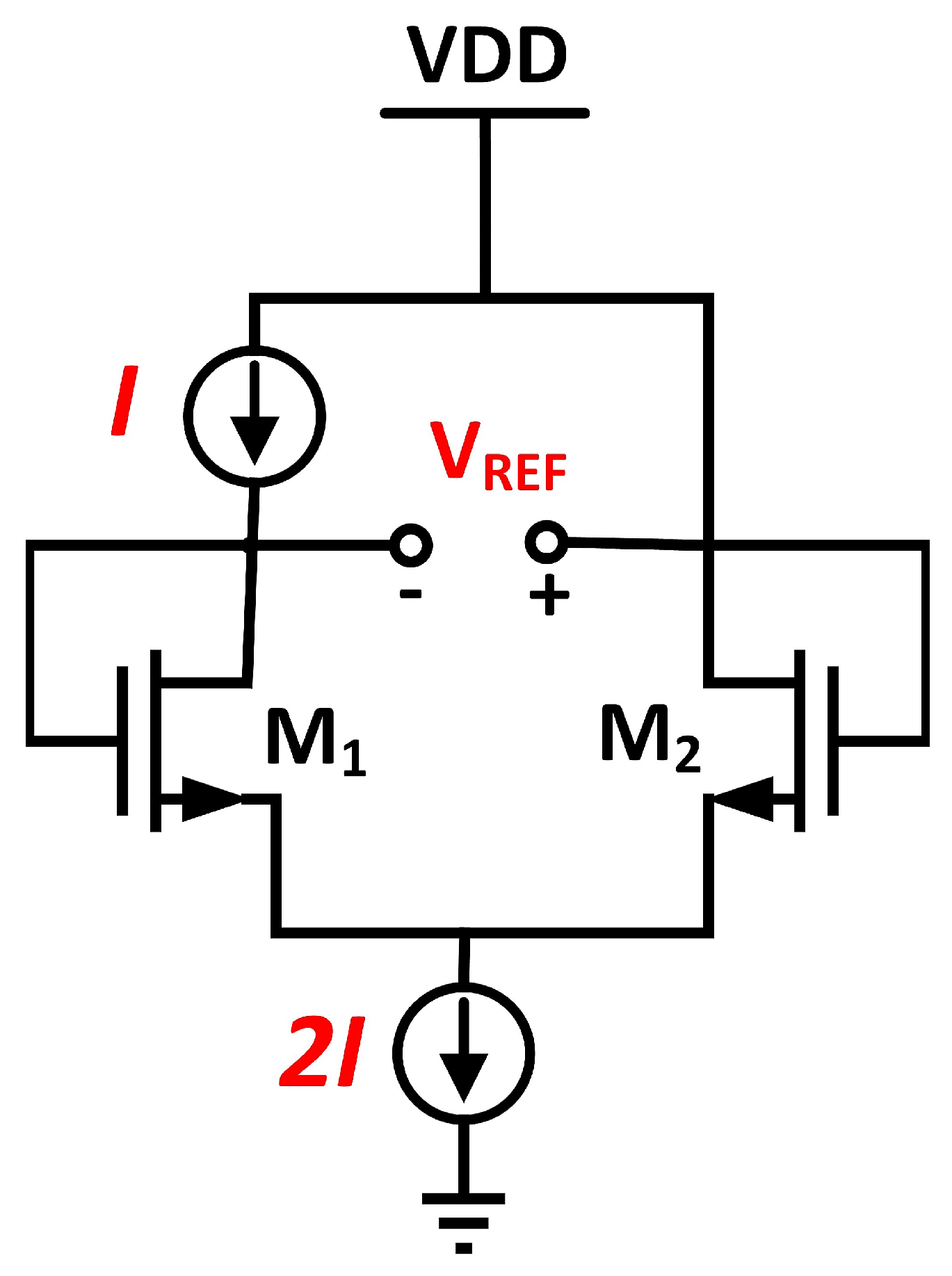
CMOS and bandgap reference are the two types of circuits widely used to provide a stable reference voltage through the process, voltage, and temperature (PVT) changes. MOSFET devices will be used in the CMOS reference circuit to represent the complementary to absolute temperature (CTAT) [
1,
2] and proportional to absolute temperature (PTAT) [
3] characteristics. The MOS transistor’s threshold voltage, Vth, determines the reference voltage while holding the CTAT characteristic with minimal temperature dependence on BJT. The simplified CMOS-based conventional voltage reference generator is depicted in
Figure 1.
The reference voltage is the voltage difference between the gate sources of two MOS transistors [
4]. Both transistors are operating in the saturation region. Equation (
1) expresses the
VREF from the two MOS transistors.
In CMOS reference, the dependency of reference voltage on temperature can be reduced by lowering the bias current,
I [
5]. In this condition, the reference voltage is approximately
VREF =
Vth2 −
Vth1. Usage of MOSFET in the reference design of CMOS will be an added advantage, as it consumes less power and allows a reduction in chip area. However, MOSFET is less sensitive to temperature, and thus it requires multiple trimming points across the process. The bandgap reference circuit has been adjusted during fabrication to produce the desired output voltage at a specific temperature. Multiple-point trimming calibrates the circuit at numerous temperature points to increase accuracy and thermal stability across a wider temperature range.
In the BGR circuit, the BJT has been used as a diode where the p-n junction of the diode is coupled with an intrinsic silicon bandgap voltage,
VBG. When the bias current is applied to the p-n junction, it produces CTAT voltage with a substantial temperature dependency. On the other hand, the design parameters can be used to adjust the temperature coefficient of a PTAT voltage to generate VBG as well [
6]. Since the BJT has higher temperature sensitivity and higher negative temperature co-efficient, it is good to inherit the replication of CTAT behavior in BGR despite it occupying a larger area on the chip and draining higher current [
5]. Besides that, the BJT transistor is the best to compensate for process variation, as it holds a single-point trimming compared to the MOSFET transistor.
As compared to the BGR architecture, the CMOS reference voltage generator has lower power consumption and occupies a smaller area. However, due to the additional
Vth as it outputs voltage headroom, it is subject to process variation. Various solutions have been proposed to solve this issue without trimming circuits, such as hybrid architecture, geometry dependence [
7], and process compensation scheme [
8,
9]. However, all these solutions have been traded off to MOSFET’s temperature coefficient.
Various techniques have been proposed to improvise the performances of BGR in the aspect of the area, power consumption, and trimming. In [
10], bandgap voltage and current references (BGVCR) technique, without an amplifier, was proposed to reduce the chip area. To produce PTAT current to guarantee the stability of the system, an amplifier was used in most BGR designs [
11]. The amplifier takes up space on the chip and degrades the accuracy of the reference voltage, owing to input offset voltage and noise. Despite eliminating the amplifier from the design, a relatively bigger area was still consumed on the chip. Apart from this, BGR with a PTAT-embedded amplifier was introduced to reduce the chip area [
12]. It consists of a single current branch that draws lower power and only consumes an area of 0.0082 mm
2. This method contributes to higher noise, as the load on the amplifier has been increased.
The resistor-less BGR circuit is another method that is widely used in BGR design. The resistor that was previously used to integrate the PTAT and CTAT voltage characteristics to create the reference voltage has been removed in this architecture. To compensate for the use of the resistor in BGR, single-branch floating PTAT voltage and PTAT voltage generators with voltage duplicator techniques were created in [
13,
14], respectively. The voltage of the bipolar transistor,
VEB, was directly floating on CTAT and was biased by a resistor-less current source in single-branch PTAT voltage, cascoded high-impedance current bias techniques. In single-branch PTAT voltage, where the voltage of a bipolar transistor,
VEB, was directly floated on CTAT and biased by a resistor-less current source, the cascoded high-impedance current bias techniques were utilized.
In [
13], the proposed voltage duplicator was multiplied by four times of PTAT, which was produced by connecting two PMOS differential pairs in series. The input of the voltage duplicator receives the bipolar transistor’s CTAT voltage or
VEB. This method aids in obviating the necessity for a resistor. The proposed methods, however, worsen the temperature coefficient performance since there is no suitable PTAT and CTAT combination to generate the reference voltage.
A resistor-less CMOS reference design has been developed to create lower power, high PSRR reference voltage for SoC applications in the MHz frequency ranges. Due to the lack of a resistor in the design, most architectures, unfortunately, have trouble providing higher-order compensation as temperature sweeps from low to high. A poor temperature coefficient results from this scenario. To address this problem, resistor-less BGR successive voltage step compensation was put forth in [
15,
16]. The PSRR is only guaranteed by this approach, however, for lower frequencies and temperature coefficients.
To overcome the aforementioned problems, this research suggests an auto-trimming BJT-based BGR with a PSRR improvement circuit. System stability is maintained without compromising BGR’s performance in terms of temperature coefficient, line regulation, and chip area. To solve the issue of process variance, the automatic trimming circuit with a straightforward comparator and network resistor has been added to the PTAT resistor. The comparator will detect when the reference voltage is out of alignment due to process variation because its input is connected to the reference voltage, and its output will activate the trimming network resistor based on the appropriate weighting to compensate for the desired output. The paper is organized as follows. The suggested BGR and circuit implementation for each block are described in
Section 2. Meanwhile,
Section 3 discusses the measurement data and analysis, and
Section 4 provides a conclusion.
2. Proposed Bandgap Voltage Reference
Figure 2 depicts the ATBGR schematic. A BGR Core (CTAT, PTAT, and op-amp), a startup circuit, a PSRR enhancement circuit, and an auto-trimming circuit are integrated. The auto-trimming circuit generates a consistent reference voltage across CMOS process variations.
2.1. Core Circuit of Bandgap Voltage Reference
Figure 3 illustrates the proposed BGR core circuit.
To design BGR with a less sensitive solution across the PVT, the circuit needs to bias itself, and the current need to independently flow to all of three branches in
Figure 3. The current mirror approach has been used to supply equal current across the CTAT, PTAT, and
VREF generator circuit. The relationship of CTAT and PTAT to
VREF is illustrated in
Figure 4.
Referring to
Figure 4, the correct pairing of the CTAT and PTAT can eliminate temperature-dependent variations and result in a stable and temperature-independent reference voltage. CTAT and PTAT node’s potential voltage is ideally equal, as shown in Equation (
2).
Since a bipolar junction transistor is employed in this design as a diode, the voltage across the diode is defined below in terms of the thermal voltage:
where
IO and
IS are the BJT’s collector current and reverse saturated current. The CTAT voltage is designated
VD, exhibiting a negative temperature coefficient (TC).
On the PTAT side, number,
n, of the bipolar transistor was added to minimize the potential voltage difference between the CTAT and PTAT. The voltage across the diode is given in (4):
Using (3) and (4), the voltage across the resistor,
R1, is derived as follows:
where
VT = kT/q, k is Boltzman’s constant, and q is the charge of the electron. Referring to (5), the voltage across the resistor,
R1, is the PTAT voltage, VPTAT. There are three branches in the core circuit, including PTAT, CTAT, and REF_GEN. All these three branches have equal bias currents, and the total current of this core circuit can be expressed in (6).
Since the voltage across the resistor,
R1, is computed using Equation (
5), and the biased current will be determined based on the design specification, the resistor,
R1, value can be obtained with Equation (
8). Equation (
8) is expressed by Substituting (7) into the result of (5).
To achieve minimal voltage variation, a total of eight bipolar transistor-based diodes are used in this design.
By assuming
VCTAT =
VD = 0.7 V as the typical diode voltage, the reference voltage of BGR is the total voltage across
R2 and
Q10, where they represent the behavior of PTAT and CTAT, respectively.
The reference voltage is derived in terms of thermal voltage,
VT, and diode voltage,
VD, as in Equation (
10).
where
and
are the weightage of PTAT and CTAT, respectively. Exhibiting zero temperature coefficient can be achieved by adding two items with the opposite temperature coefficients with the appropriate weight, as expressed in Equation (
11).
Since CTAT has only one diode, the CTAT weightage,
= 1. Based on [
16], the (
VT)/(
T) = 85 µV/°C) and (
VD)/(
T) = −1.63 mV/°C), by substituting into (11), the PTAT weightage,
, will be computed as 18.82. The PTAT weightage,
, is equivalent to
VR2 because it replicates the behavior of the PTAT as it is defined in (9). The voltage across the resistor,
VR2, is expressed as in (12).
Since all three branches flow the same current, by substituting Equation (
7) into Equation (
12),
R2 can be determined.
R1 and
R2 play a critical role in determining the reference value. A trimming circuit has been implemented on
R2 to ensure the reference voltage is independent of the process variation.
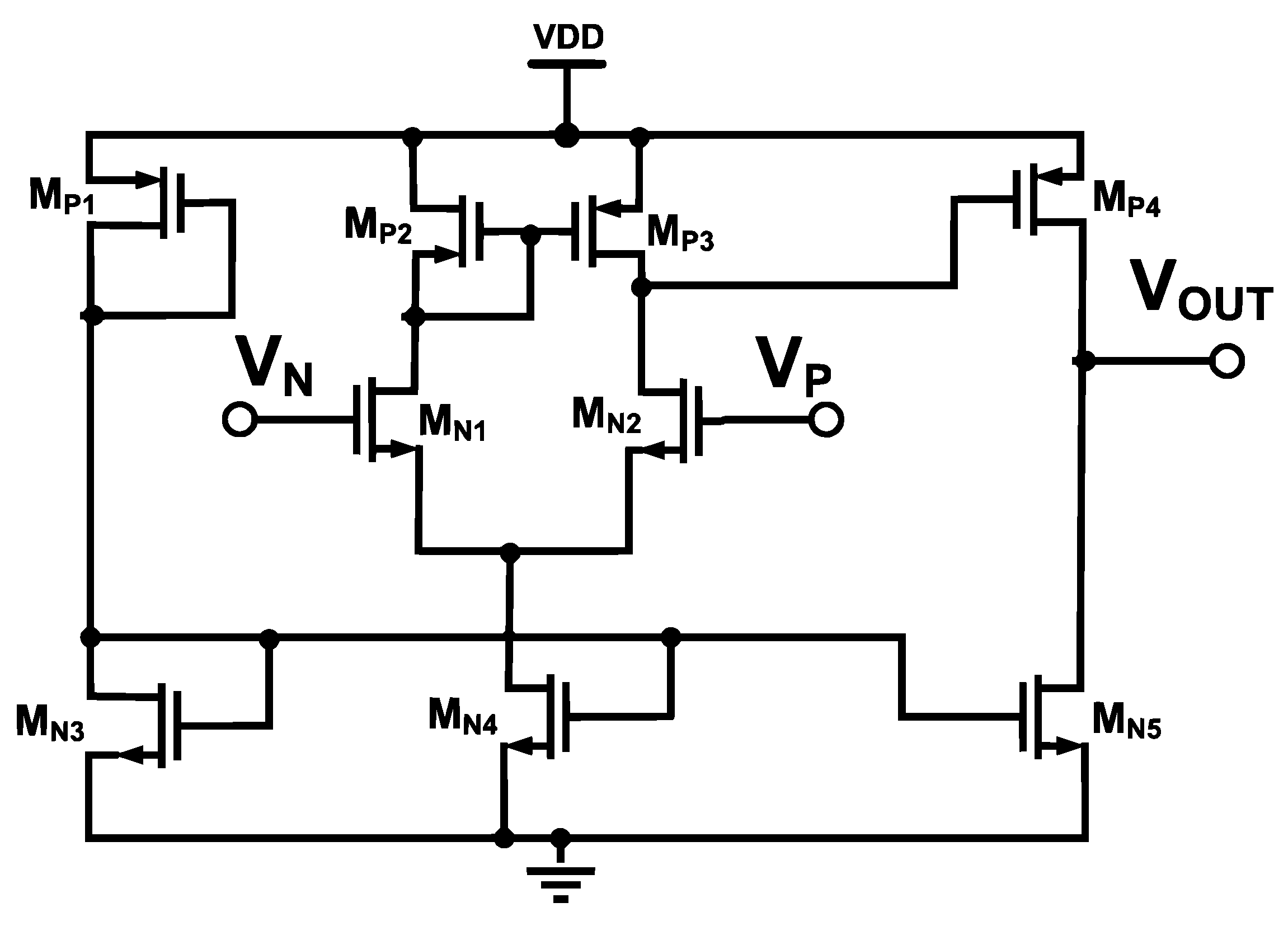
2.2. Two-Stage Operational Amplifier with Active Miller Compensation (AMC)
In our BGR, a two-stage op-amp is used to achieve the design goal of equal CTAT and PTAT potential differences. The schematic of the design is illustrated in
Figure 5. If the amplifier detects inequality, the output of the amplifier will trigger the gate of current mirror M
8 and M
9 to increase the drain current to equalize the voltage differences.
Figure 6 illustrates the simulated input voltages of the amplifier across the temperature. The simulated input voltages of the amplifier exhibit linear characteristics from −40 °C to 125 °C while generating the reference voltage with CTAT and PTAT. A stable and constant output voltage is produced because CTAT and PTAT are tied to each amplifier node.
The two-stage op-amp consists of a differential single-ended output with current mirror biasing as the first stage and a common source stage as the second stage. Its transfer function is given as follows:
The gain of the op-amp is expressed as follows:
Referring to
Figure 5, the integrated M
F acts as an AMC for the high-gain op-amp. Operating comfortably in the saturation region due to high overdrive gate voltage from VDD contributes to higher active RC, which is inherited from M
F. Higher RC moves the dominant pole away towards low frequency, thus improving the phase margin.
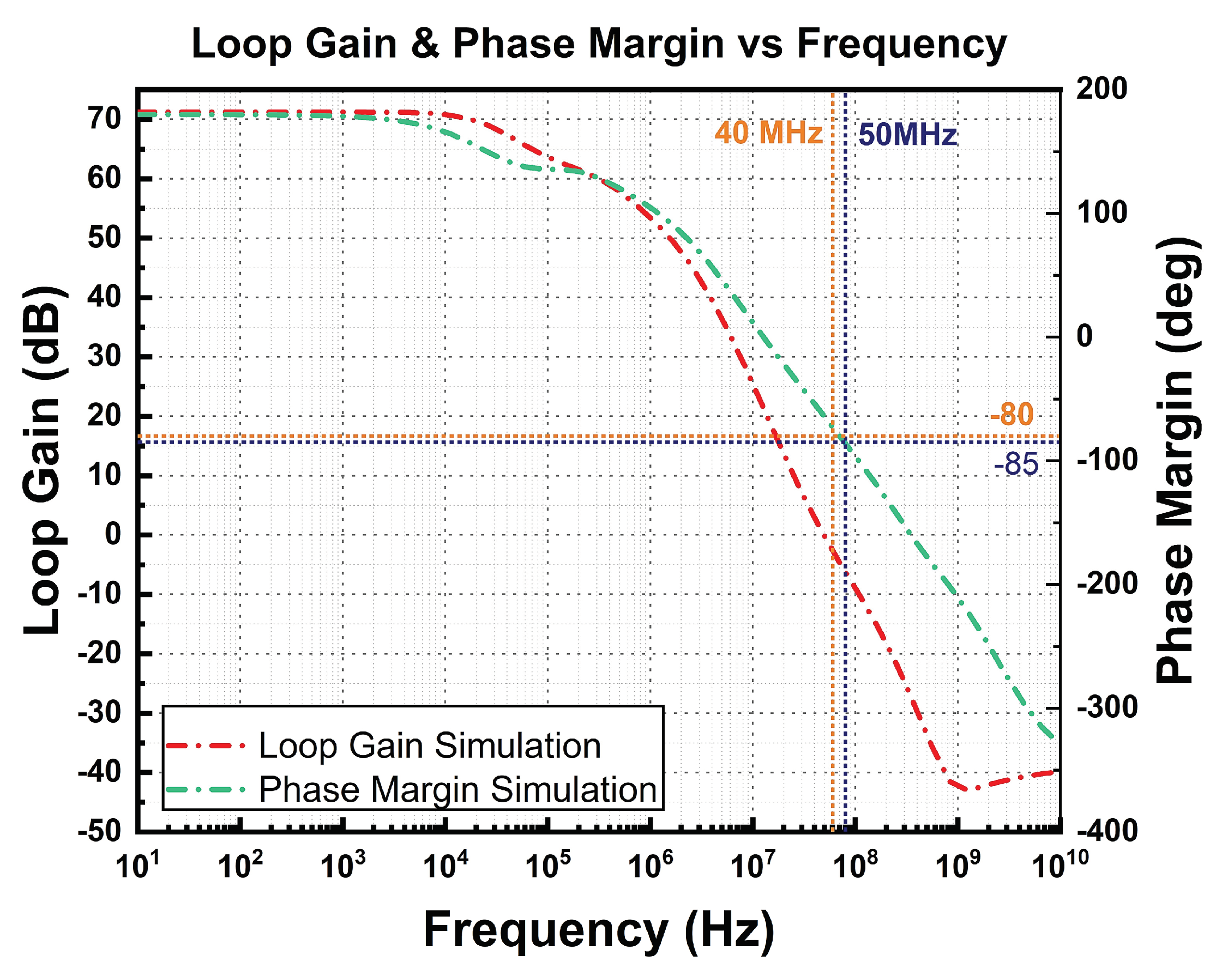
Figure 7 illustrates the simulation results of the two-stage op-amp’s corresponding open-loop gain and phase margin. The maximum achieved is 64 dB with a phase margin of 60°.
The active miller compensation with integrated MF helps to move the dominant pole to a higher frequency, that is, from 40 MHz to 50 MHz, and achieves a phase margin of 60 degrees, which is a stable condition.
2.3. Startup Circuit
Figure 8 illustrates the proposed startup circuit for the ATBGR.
The startup circuit consists of three PMOS transistors, a NMOS transistor, and a resistor, R3, designed to break the zero-current region into the normal operating region. VN of M1 is connected to the startup circuit.
When the BGR core circuit is turned to normal operation mode, all transistors in the startup circuit are in hibernate mode, as condition VN is zero current state. Only the transistor, M18, is ON, and the current starts to flow on the VN node.
As a result, the amplifier will perform a comparison between
VN and
VP nodes, respectively, and correct another node by increasing the current flow through M
12 of the core circuit, leading to an equal flow of current on both of nodes. As the input node of the amplifier starts to flow the current, the gate voltage of the M
19 is in a “HIGH” state, enabling current mirror pair M
16–M
17. As a result, M
18 is turned off, thus switching the startup circuit to hibernating mode.
Figure 9 illustrates the simulated transient response of the ATBGR with and without the startup circuit.
The ATBGR quickly reaches a steady state after the startup circuit exits the zero-current region. On the other hand, without the startup circuit, it takes longer to reach a steady state, as depicted in
Figure 9, as the amplifier’s input node was initiated by itself to break the zero-current region.
2.4. Auto-Trimming Circuit
Figure 10 illustrates the auto-trimming circuit integrated into the ATBGR to resolve the reference voltage variation issue across the process.
R2 is used for the trimming purpose, referring to (12). A 4-bit trimming circuit has been integrated with
R2. The value of the resistor is an increment from one to another in multiples of two, that is,
R, 2
R, 4
R, and 8
R, each connected in parallel to the PMOS switches M
20–M
23. PMOS is favorable over NMOS, as it exhibits reduced process sensitivity.
The trimming action is automated in the auto-trimming circuit (ATC) through built-in op-amps 1 and 2. The op-amps compare an external voltage, +1.25V_EXT, 1.25 V, with the reference voltage, VREF, to detect and reduce the variation. This external voltage was supplied from an external DC power supply model (Agilent-E3631A). In this design, two op-amps were used to capture the variation range.
The first op-amp was used to record any events where the output voltage was marginally higher than the external voltage. When the reference voltage is greater than the external voltage, the op-amp will be set. The negative op-amp node is connected and attached to the external voltage, +1.25V_EXT, while a positive node is connected to the VREF output of the BGR core.
Op-amp 2 is used to determine whether the output voltage was less than the external voltage. When the output voltage is less than the external voltage, the op-amp will set. The output of the BGR was connected to its negative node and an external voltage, +1.25V_EXT, is connected to the positive node. When the output voltage of the BGR exceeds the external reference voltage, the resistors R and 2R are configured, whereas larger resistances, such as 4R and 8R, are configured when the output voltage is lower. The transistor-level schematic of the op-amp is shown in
Figure 11.
The 2-to-4 demultiplexer is used to control the resistor network through the PMOS switches. The output of the op-amps is used as the selection pin of the de-multiplexer. The MOSFET switches will be configured according to the response of the op-amp. The trimming step for the 4-bit trimming circuit is 110 µV/LSB. The truth table of the 2-to-4 demultiplexer is shown in
Table 1.
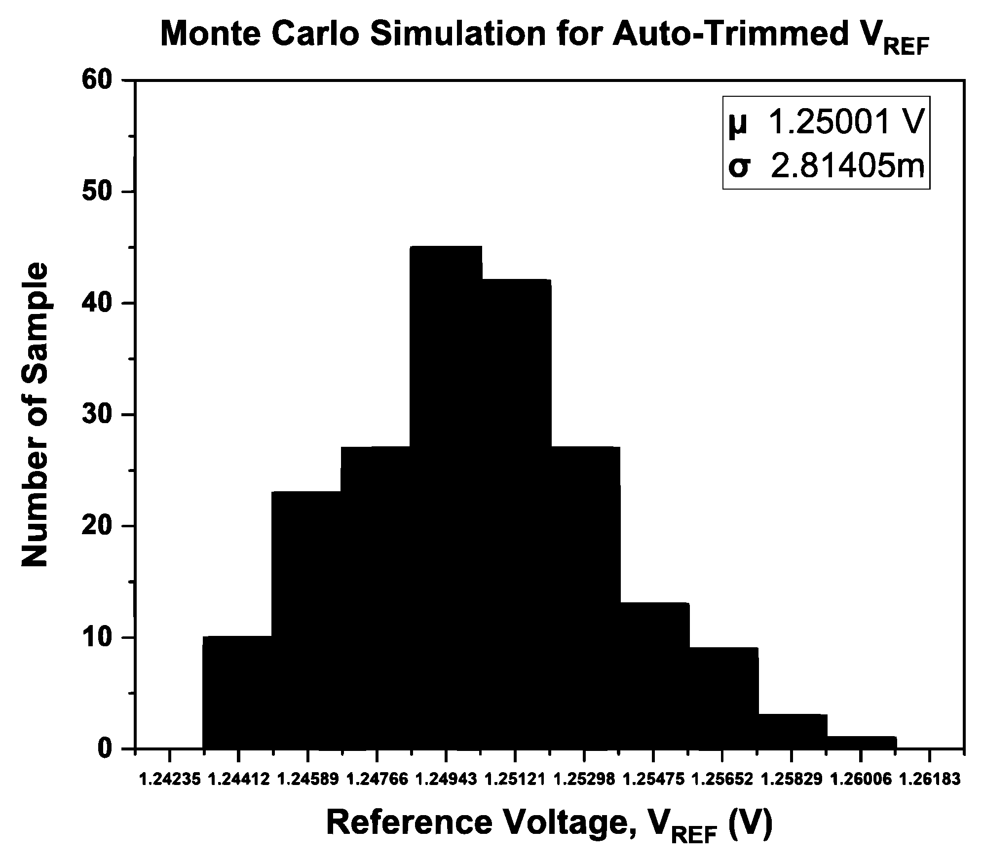
To verify the effectiveness of the ATC, a Monte Carlo simulation has been performed for 200 samples. The Monte Carlo simulation was used to analyze the normal distribution of both with and without the ATC, and the results are illustrated in
Figure 12 and
Figure 13, respectively.
Referring to
Figure 12 and
Figure 13, the BGR with ATC achieves
VREF with higher precision (1.25001 V) than without ATC (1.25156 V). According to the findings, the ATBGR with ATC-distributed data is close to the mean value compared to the ATBGR without ATC. ATC has resulted in a normal distribution. Furthermore, the latter has a lower standard deviation than the former.
2.5. PSRR Enhancement Circuit
To enhance the PSRR performances in the BGR circuit at a higher frequency range, a cascaded PMOS common gate pair has been integrated at the output of the BGR, as illustrated in
Figure 2.
An analysis model of the BGR is illustrated in the
Figure 14 below.
In the figure,
Zout is the output impedance of the BGR and
ZBGR is the shunting effect of its feedback loop.
Zout and
ZBGR are given as follows:
where
and
From here,
VREF is calculated as
and PSRR is obtained as
The simulation results of the PSRR with and without the PSRR enhancement circuit are illustrated in
Figure 15. It can be observed that the enhancement circuit improves the rejection significantly at a frequency of more than 1 KHz.
3. Measurement Results
The proposed BJT-based BGR has been designed and fabricated in 0.18 µm CMOS technology. The chip area of the BGR is 0.032768 mm
2, including the bond pads for measurement.
Figure 16 depicts the photomicrograph of the proposed BJT-based BGR with the bond pads.
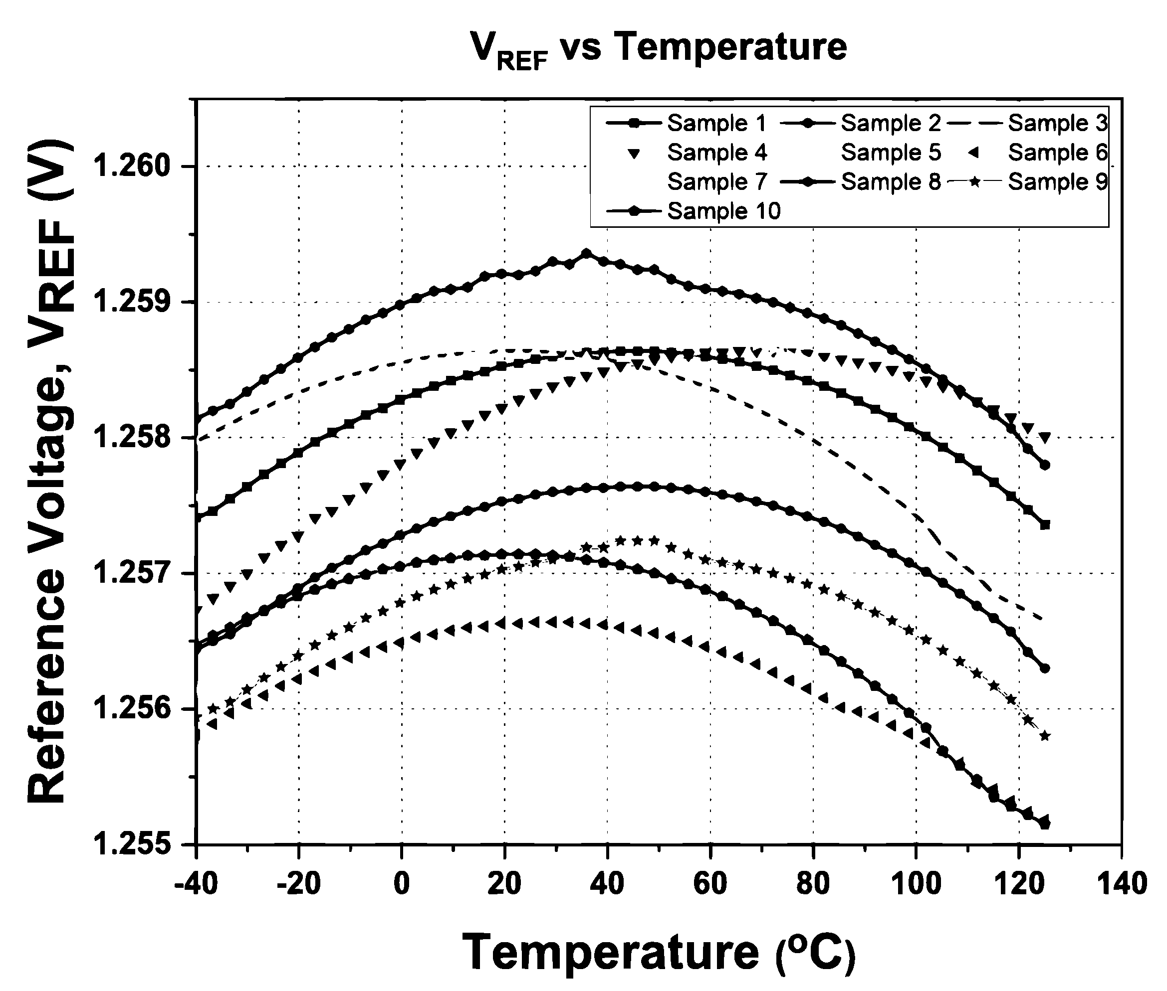
To validate the proposed BGR design, a total of 10 samples of the chip were measured. The 10 samples are selected from various wafers that fall under the FF, TT, and SS speed grades.
Figure 17 shows the output voltage of BGR with a temperature range from −40 °C to 125 °C with a supply voltage of 3.3 V. The BGR was designed to generate 1.25 V as an output voltage. The output voltage of the proposed BGR has a deviation smaller than 1.278 mV across the temperature ranging from −40 °C to 125 °C. Based on the 10 samples, the minimum and maximum temperature coefficients are 6.11 ppm/°C and 15.32 ppm/°C, respectively, with power supply ranges from 1.65 V to 4.5 V. The proposed BGR core circuit only consumes 16.4 µA when the input supply is 3.3 V.
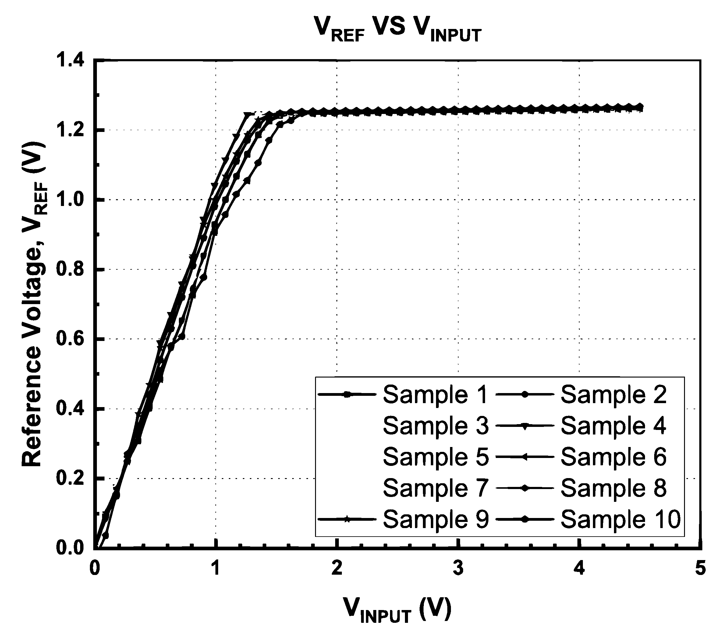
Additionally, the input voltage variation is also taken into consideration in this proposed BGR circuit.
Figure 18 shows the output voltage of BGR with swiping the input supply from 0 V to 4.5 V. The output voltage starts to become saturated when the input supply is 1.65 V and remains in the saturation region up to 4.5 V. During this saturation period, the deviation of the output voltage is only 15.47 mV. The measured line regulation of the output voltage is 0.434%/V across the power supply of 1.65 V to 4.5 V.
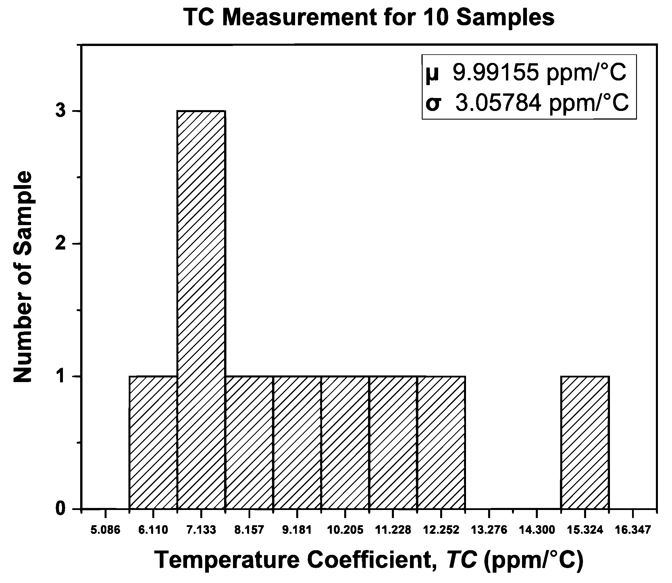
The performance distribution of the proposed BGR for the ten samples after trimming was extracted from
Figure 17 and
Figure 18, and the distribution of
VREF and the temperature coefficient is shown in
Figure 19 and
Figure 20, respectively.
Figure 19 illustrates the measured mean output reference voltage at room temperature, that is, 1.2495 V with a standard deviation of 2.38 mV. The measured TC distribution is depicted in
Figure 20 and has a mean value of 9.99 ppm/°C and a standard deviation of 3.06 ppm/°C.
The measured results of the PSSR of the proposed BGR circuit are shown in
Figure 21. The PMOS PSRR enhancement circuit helps to optimize the PSRR of the BGR circuit across the frequency, especially in the higher frequency range.
The measurement results are compared against other BGRs from the literature in
Table 2. With a supply headroom range of 1.65 V to 4.5 V and a reasonable temperature coefficient, the proposed BGR provides the best PSRR at higher frequency ranges.

 ,
, 


