Article

Novel SiGe/Si Heterojunction Double-Gate Tunneling FETs with a Heterogate Dielectric for High Performance

1
School of Electronic Engineering, Xi’an University of Posts & Telecommunications, Xi’an 710121, China
2
Nova Product Line, Xi’an Huawei Technologies Co., Xi’an 710065, China
*
Authors to whom correspondence should be addressed.
Micromachines 2023, 14(4), 784; https://doi.org/10.3390/mi14040784
Submission received: 5 March 2023 / Revised: 22 March 2023 / Accepted: 27 March 2023 / Published: 31 March 2023

Abstract

:
In this paper, a new SiGe/Si heterojunction double-gate heterogate dielectric tunneling field-effect transistor with an auxiliary tunneling barrier layer (HJ-HD-P-DGTFET) is proposed and investigated using TCAD tools. SiGe material has a smaller band gap than Si, so a heterojunction with SiGe(source)/Si(channel) can result in a smaller tunneling distance, which is very helpful in boosting the tunneling rate. The gate dielectric near the drain region consists of low-k SiO2 to weaken the gate control of the channel-drain tunneling junction and reduce the ambipolar current (Iamb). In contrast, the gate dielectric near the source region consists of high-k HfO2 to increase the on-state current (Ion) through the method of gate control. To further increase Ion, an n+-doped auxiliary tunneling barrier layer (pocket)is used to reduce the tunneling distance. Therefore, the proposed HJ-HD-P-DGTFET can obtain a higher on-state current and suppressed ambipolar effect. The simulation results show that a large Ion of 7.79 × 10⁻⁵ A/μm, a suppressed Ioff of 8.16 × 10⁻¹⁸ A/μm, minimum subthreshold swing (SSmin) of 19 mV/dec, a cutoff frequency (fT) of 19.95 GHz, and gain bandwidth product (GBW) of 2.07 GHz can be achieved. The data indicate that HJ-HD-P-DGTFET is a promising device for low-power-consumption radio frequency applications.

1. Introduction

With continuous improvements in chip integration and application requirements, the dimensions of conventional MOSFETs are continuously scaling down to a few nanometers. This results in a number of critical issues, such as leakage current, high-power dissipation, short channel effects (SCEs), and a sub-threshold slope restriction of 60 mV/decade for conventional MOSFETs at room temperature [1,2,3,4,5]. Moreover, the contradiction between static power consumption and device performance caused by off-state leakage current has become a serious problem.
To overcome the limitations of conventional MOSFETs, many novel device structures have been proposed in the past couple of years. Tunnel field-effect transistors (TFETs), one of the most promising candidates for MOSFETs, have been attracting more and more attention in recent years. Because the high-energy tail states of the Fermi distribution function in the source are removed, the off-state current (Ioff) of TFETs is much lower than that of the MOSFETs [6]. In addition, because band-to-band tunneling (BTBT) is the main operation mechanism in TFETs, they can break the limitation of 60 mV/decade subthreshold swing (SS) in conventional MOSFETs, which relies on hot electron emission, especially at low voltages [7,8]. Finally, TFETs are more immune to short channel effects and temperature variations [9,10]. Therefore, these advantages make TFETs more favorable for circuits that are based on low-power applications.
However, the main problems of TFETs are low on-state current (Ion), high off-state current (Ioff), and ambipolar behavior, which are the main challenges that traditional TFETs face [11,12,13]. The driven current of the conventional TFETs is determined by the gate-modulated tunneling diode. Furthermore, for the silicon-based TFET, the large bandgap and carrier mass in silicon material result in a small drive current. Thus, double-gate tunnel field-effect transistors (DGTFETs) are expected to extend the limitations of leakage current and subthreshold slope [10,14,15,16]. At present, various methods, such as gate dielectric engineering [17,18,19,20], hetero-structure [21,22,23,24], dielectric pocket [25,26,27,28,29] and work function engineering [15,30,31,32], are proposed to improve the Ion. However, most of these approaches significantly boost Ion at the expense of other device performance metrics, such as Ioff, ambipolar current, and analog/RF performance.
Going forward, silicon germanium (SiGe) will most likely be adopted for future low-power very-large-scale integration (VLSI) technologies among all material systems for TFET applications, owing to its VLSI compatibility, mature synthesis techniques, and tunable bandgap [11,33,34]. In this work, we propose a new Si1-xGex/Si heterostructure TFET with high-k/low-k dual material heterogeneous gate dielectric and a heavily doped pocket within the channel (HJ-HD-P-DGTFET). The use of p-type doped SiGe material in the source region instead of adopting germanium and III-V compound semiconductors in the source region of TFET can lead to higher ON/OFF ratios due to a smaller tunneling distance obtained by the heterojunction, which is very helpful to boost the tunneling rate [15]. Furthermore, an n+-doped auxiliary tunneling barrier layer (pocket) is added between the source/channel junction to further increase tunneling efficiency of the device at the tunnel junction [35]. Finally, the gate dielectric near the drain region consists of SiO2 with low K values, which weakens the gate control of the channel-drain tunneling junction and can effectively reduce the ambipolar current (Iamb), while HfO2 with a high K value near the source region is chosen to increase Ion through the method of gate control [36,37].
The structures of this paper are as follows: Section 2 incorporates the proposed device structure along with the design parameters, simulation models, and fabrication process. Section 3 is dedicated to the mechanism, characteristics, and analog/RF performance of the proposed devices (HJ-HD-P-DGTFET). The device parameter variability analysis of the proposed structure is also covered in this section. Furthermore, a performance comparison between Si DG-TFET and HJ-HD-P-DGTFET is also carried out in this section. Finally, Section 4 summarizes the conclusions of this work.

2. Device Architecture, Parameters, and Simulation Methods

A schematic diagram of the HJ-HD-P-DGTFET structure is shown in Figure 1, which has two symmetrical gate regions to increase the Ion. In the proposed TFET, Si0.6Ge0.4(source)/Si(channel) heterojunction is used to increase the drain current. The source/drain regions are symmetrically located on both sides of the channel, and the p-Si channel is inserted below the gate. Doping is performed in such a way so as to obtain maximum Ion current. Here, we doped the p+ source region with 1 × 10²⁰ atoms/cm3, n+ drain region with 1 × 10¹⁸ atoms/cm3, n+ pocket region with 1 × 10¹⁸ atoms/cm3, and the intrinsic channel with 1 × 10¹⁶ atoms/cm3. Moreover, a conventional Si-DGTFET is used for comparison. All of the device parameters used in the simulation process are given in Table 1.
The device simulations are carried out using a Synopsys Sentaurus device simulator, which solves Poisson’s equation self-consistently with the carrier current continuity equations. The nonlocal BTBT model is used in the simulations to take spatial variation in the energy band into account, and it also considers that the generation/recombination of the opposite carrier type is not spatially coincident. Therefore, the BTBT tunneling process is modeled more accurately. The Shockley–Read–Hall (SRH) and Auger recombination models are considered to include the effect of carrier recombination. The band gap narrowing model and Fermi–Dirac statistics are included because the source regions are highly doped. Moreover, the concentration-dependent and field-dependent mobility models are also adopted in the simulations.
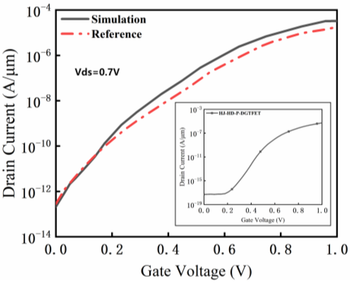
For validation of the models used in the Sentaurus TCAD tool, we calibrated our model against the work carried out by Narang R et al. [38]. Figure 2 shows our model calibration against the work carried out by Narang R et al. [38]. Good agreement between the simulated data and the reported results was observed. The inset shows the simulation result of the transmission characteristics of the HJ-HD-P-DGTFET. It is observed that the Ion of the HJ-HD-P-DGTFET can reach 7.79 × 10⁻⁵ A/μm, and the Ioff is only 8.16 × 10⁻¹⁸ A/μm. Additionally, the subthreshold swing (SS) of the device is only 19 mV/dec.
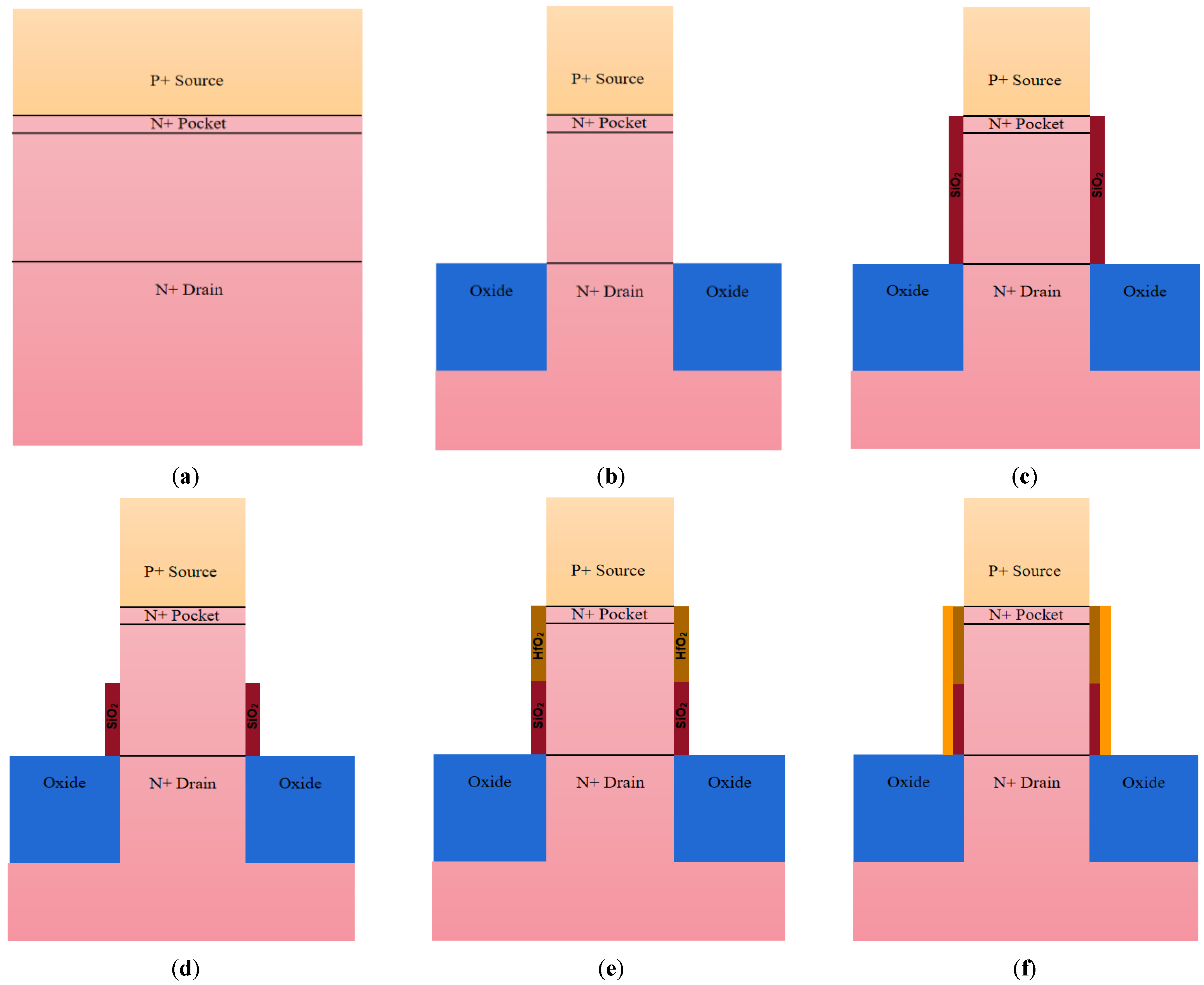
The proposed HJ-HD-P-DGTFET structure can be fabricated using similar steps as reported for DGTFET [1,2]. The possible fabrication steps of the proposed HJ-HD-P-DGTFET are shown in Figure 3. The process begins by preparing the silicon substrate; then, the n+ drain doping region is introduced by vertical As implantation and annealing. Afterward, a thin layer of the n+ pocket is grown via epitaxy. Next, the source region is implanted, as shown in Figure 3a. Following this, the channel region is formed by etching. Subsequently, the isolation oxide is deposited to prevent the drain region from etching, as shown in Figure 3b. In Figure 3c, SiO2 can be grown on the channel using an oxidation process. In Figure 3d, the SiO2 gate dielectric is selectively etched away at the source side by using buffered hydrogen fluoride (BHF) solution. The SiO2 gate dielectric at the drain side is protected by photoresist masks. Part of the SiO2 gate dielectric layer will be replaced by high-k material in Figure 3e. For the next step, atomic layer deposition (ALD) of high-k material HfO2 is performed to fill the gap. After this, HfO2 is deposited by ALD on the silicon surface to form a heterogeneous gate dielectric. In Figure 3f, the remaining processes are similar to conventional vertical TFET, involving gate deposition, silicon exposure, etc. [39,40].

3. Results and Discussion

This section analyzes the comparison between Si-DGTFET and HJ-HD-P-DGTFET. Additionally, the effects of device parameters on the transfer characteristics are analyzed, such as the Si1-xGex/Si heterojunction, heterogeneous gate dielectric, and pocket. Finally, the RF performance of HJ-HD-P-DGTFET is also analyzed.

3.1. The Physical Characteristics of Si-DGTFET and HJ-HD-P-DGTFET

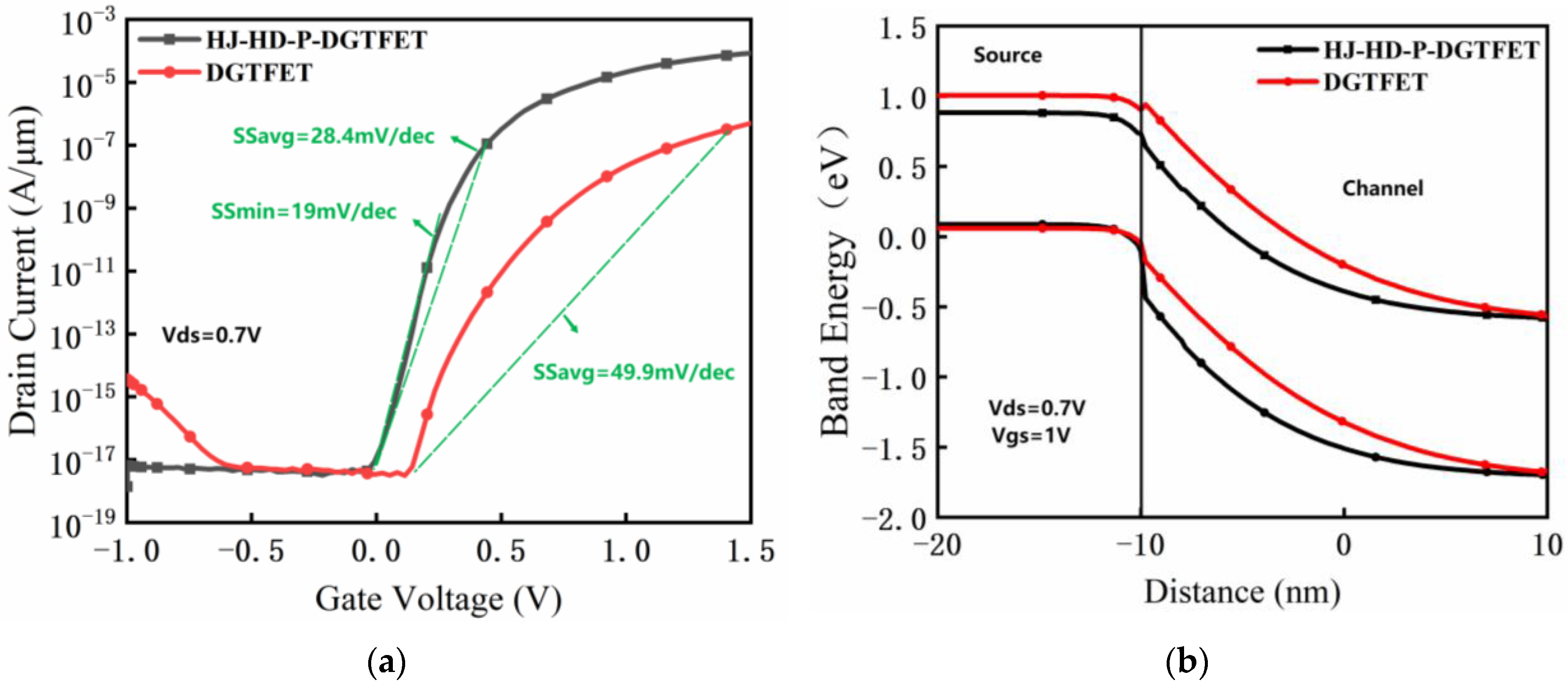
Figure 4a compares the transfer characteristics of HJ-HD-P-DGTFET and conventional Si-DGTFET. Due to the use of a SiGe/Si heterostructure and auxiliary tunneling barrier layer (pocket) of n+-doped material, which can increase the tunneling rate, the HJ-HD-P-DGTFET reaches an on-state current (Ion) of 8.46 × 10⁻⁵ A/μm compared with 2.83 × 10⁻⁶ A/μm for the conventional Si-DGTFET. It is observed that the Ion for HJ-HD-P-DGTFET is increased by nearly two orders of magnitude compared to conventional Si-DGTFET. Furthermore, a minimum subthreshold swing (SSmin) of 19 mV/dec and an average subthreshold swing (SSavg) of 28.4 mV/dec are obtained, while the SSavg of the conventional Si-DGTFET is 49.9 mV/dec. As a result, HJ-HD-P-DGTFET has obvious improvements in Ion and subthreshold swing compared to conventional Si-DGTFET. Finally, the ambipolar effect for HJ-HD-P-DGTFET is noticeably suppressed, as shown in Figure 4a. Figure 4b shows the on-state energy band condition of both HJ-HD-P-DGTFET and Si-DGTFET. It can be observed that in the on-state, the tunnel barrier of HJ-HD-P-DGTFET is evidently narrower than conventional Si-DGTFET at the channel and source junction.

3.2. Si1-xGex/Si Heterojunction

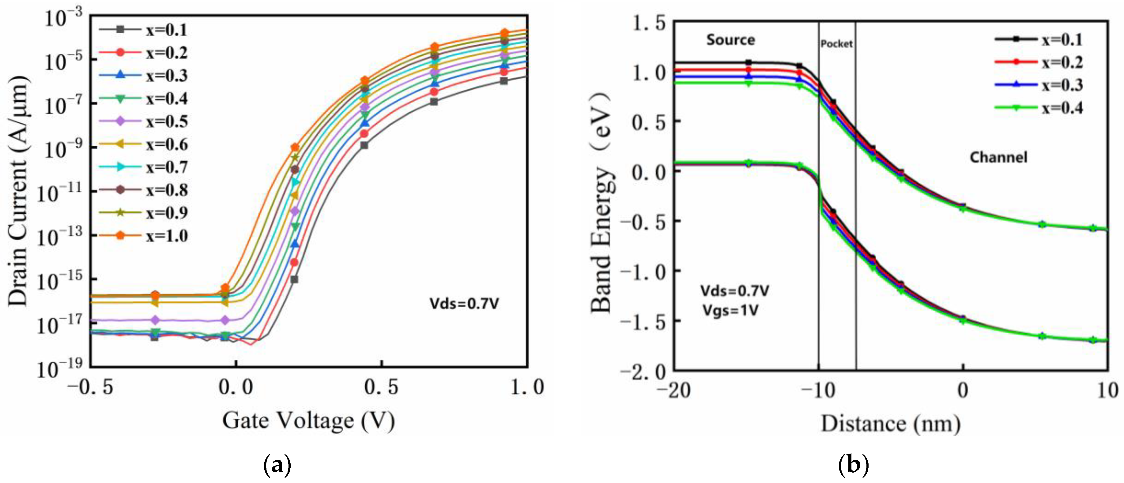
As discussed in Section 2, the source region formed by Si1-xGex is used to improve the on-state current in the HJ-HD-P-DGTFET. It is essential to study the variation in the current value with the different germanium compositions in Si1-xGex, where Si1-xGex (x = 1) equals Ge. Figure 5a depicts the effect of different Ge compositions in the Si1-xGex source region on transfer characteristics, and it is very clear that the on-state current of the proposed device increases with the increase in x until x = 1. When the mole fraction of germanium is 0.1, the on-state current is approximately 1 × 10⁻⁵ A/μm. Furthermore, the on-state current reaches about 8 × 10⁻⁴ A/μm when the mole fraction is increased to 0.9. However, the increase in the Ioff is much greater than the increase in the Ion when the mole fraction is greater than 0.4. Figure 5b shows the effect of the composition ratio x of Si1-xGex on the on-state energy band diagram of HJ-HD-P-DGTFET. As can be seen from this figure, the energy valley value of the conduction band decreases with an increase in the germanium composition. Tunneling is defined as the injection of electrons from the source valence band to the channel conduction band. The smaller energy valley value of the conduction band in the source region represents the larger band-to-band tunneling rate without varying other conditions. Thus, x = 0.4 in Si1-xGex makes a shorter tunneling width compared to other compositions. Consequently, x = 0.4 is chosen as the optimal value in Si1-xGex to ensure a lower off-state leakage current and a higher on-state current.
Figure 6a–d show the transfer characteristics, on-state energy band diagram, electric field, and potential with different doping concentrations in the source region (Ns) when the mole fraction of germanium in Si1-xGex is 0.4. It is observed that the off-state current is decreased, while the on-state current increases as a result of higher source region doping concentration Ns. However, the on-state current slightly decreases when Ns increases from 1 × 1020 cm−3 to 8 × 1020 cm−3. It is evident that the maximum value of the Ion occurs at a concentration of 1 × 1020 cm−3, and the corresponding Ion is 1.05 × 10⁻⁴ A/μm, as shown in Figure 6b. It is also observed that the tunneling distance at the point of the tunnel junction decreases with an increase in the source region doping concentration Ns. Furthermore, the valence band increasing significantly in the source region leads to a smaller tunneling distance when Ns is 8 × 1020 cm−3. Meanwhile, there is a very large tunneling distance when Ns is 5 × 1018 cm−3, which diminishes electron BTBT rates. The value of the electric field under the pocket and channel (–10 nm–10 nm) increases as a result of higher source region doping concentration Ns, as seen in Figure 6C. Consequently, the increasing electric field under the pocket can help to improve the tunneling probability in this region, while increasing the electric field under the channel will raise the barrier height in the drain/channel interface. However, it is observed in Figure 6b that the conduction band spike at the SiGe/Si heterojunction interface appears when the Ns is more than 1 × 1020 cm−3, which leads to the carriers that pass through barriers being recombined with the opposite carriers at the interface. This results in the on-state current slightly decreasing when the source region doping concentration Ns exceeds 1 × 1020 cm−3. Therefore, the maximum current is attained at Ns = 1 × 1020 cm−3.

3.3. Gate Heterogeneous Dielectric Structures

Figure 7a shows the transfer characteristic curve of the HJ-HD-P-DGTFET with heterogeneous gate dielectric structure (HfO2 + SiO2 or SiO2 + HfO2) and single gate dielectric material (HfO2 or SiO2). As shown in Figure 7a, it was observed that the Iamb of HJ-HD-P-DGTFET with a heterogeneous gate dielectric structure (HfO2 + SiO2) and the single gate dielectric material with SiO2 decrease by about three orders of magnitude compared with heterogeneous gate dielectric structure (SiO2 + HfO2) and the single gate dielectric material with SiO2 when Vgs = −1 V. This indicates using SiO2 for the gate oxide layer near the leakage region effectively inhibits the ambipolar behavior of the device in the heterogeneous gate dielectric structure (HfO2 + SiO2). The Ion of the HJ-HD-P-DGTFET with heterogeneous gate dielectric structure (HfO2 + SiO2) increases by four orders of magnitude compared with the single gate dielectric material (SiO2) when Vgs = 0.5 V, indicating that the gate oxide layer using HfO2 near the source region can effectively improve the open current of the device. Therefore, the combined heterogate dielectric structure of HJ-HD-P-DGTFET can not only suppress the ambipolar behavior but also improve the on-state current.
Figure 7b shows the transfer characteristics of HJ-HD-P-DGTFET with different gate dielectric thicknesses (To). As can be seen from the figure, the Ion of HJ-HD-P-DGTFET decreases with increasing gate oxide thickness. The maximum Ion of HJ-HD-P-DGTFET decreases from 1.38 × 10⁻⁴ A/μm to 1.18 × 10⁻⁵ A/μm when the gate dielectric thickness varies from 1 to 6 nm. Furthermore, the ambipolar current of HJ-HD-P-DGTFET with To = 1 nm increases by two orders of magnitude compared with To = 6 nm. Figure 7c explains Figure 7b from the electric field distribution with different gate dielectric thicknesses. It is observed that the maximum electric field at the source/pocket interface (−10 nm to −6 nm) increases with decreases in gate dielectric thicknesses, thus reducing the tunneling distance and improving the on-state current. In addition, the electric field at the drain/channel tunnel junction (10 nm) decreases with decreases in gate dielectric thickness, which weakens the band bending around the drain/channel tunnel junction and also reduces the tunneling window. Consequently, the tunneling probability of the carriers is reduced. and the Iamb is also weakened with the increases in gate dielectric thickness at the drain/channel tunnel junction. The larger ambipolar current at To = 1 nm is due to the interface trap at the gate oxide layer, which results in strong electric field bending. Considering the results above and the process conditions, a gate oxide thickness of 2 nm is considered more appropriate. Figure 7d shows the transfer characteristics of HJ-HD-P-DGTFET with different gate work function (ΦM). Firstly, the selection of ΦM is critical for the Ioff, which increases rapidly with decreases in ΦM, as depicted in Figure 7d. Secondly, the Ion of HJ-HD-P-DGTFET increases slowly with decreases in ΦM. Hence, taking into account the two factors, the optimal value of ΦM is chosen as 4.3 eV.

3.4. Auxiliary Tunneling Barrier Layer (Pocket) Optimization Results

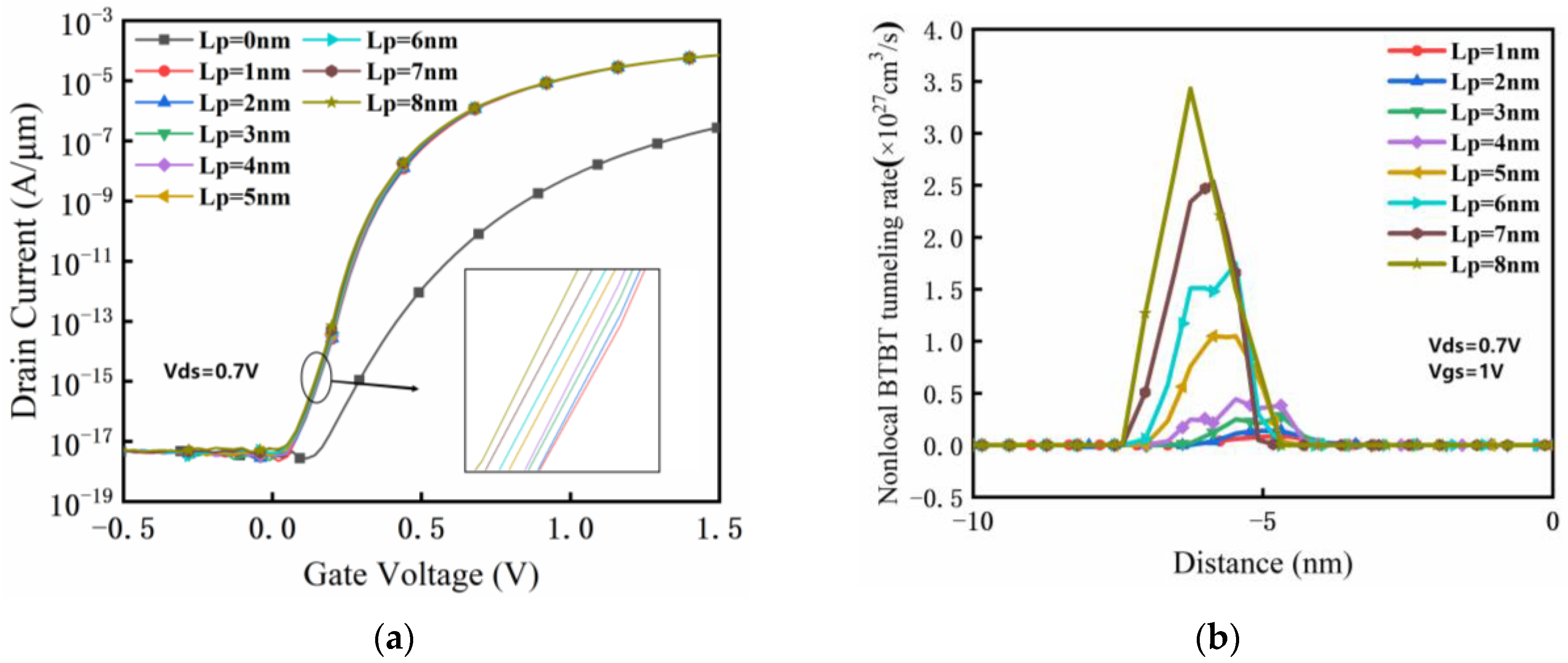
In order to improve the performance of the device, we introduced a structure with a lightly doped pocket near the source region in the HJ-HD-P-DGTFET. The proposed device is optimized for pocket length (LP) by varying its value from 0 nm (without pocket) to 8 nm. When LP was varied in the channel region, the height of the pocket (Tp) was kept constant at 20 nm. All the other design parameters are the same as listed in Table 1.
Figure 8 shows the effect of the pocket structure parameters on device performance. It can be seen from Figure 8a that the pocket can effectively improve the transfer characteristics of the device. The Ioff shows a slight dependence on pocket length, while Ion and SS values are independent of pocket length LP, as shown in Figure 8a. It is clear that there is no obvious change in Ion, but Ioff slightly increases as LP increases from 1 nm to 8 nm. The Ioff increases from 2.4 × 10⁻¹⁸ A/μm to 8.5 × 10⁻¹⁶ A/μm with the increase in Lp from 1 nm to 8 nm. As seen in Figure 8b, the BTBT tunneling rate at the source channel junction is reduced with LP and extends towards the channel side, which eventually reduces Ioff with LP in the device. Therefore, 2 nm is considered as the optimum length of the pocket in order to obtain a lower Ioff and good process conditions.
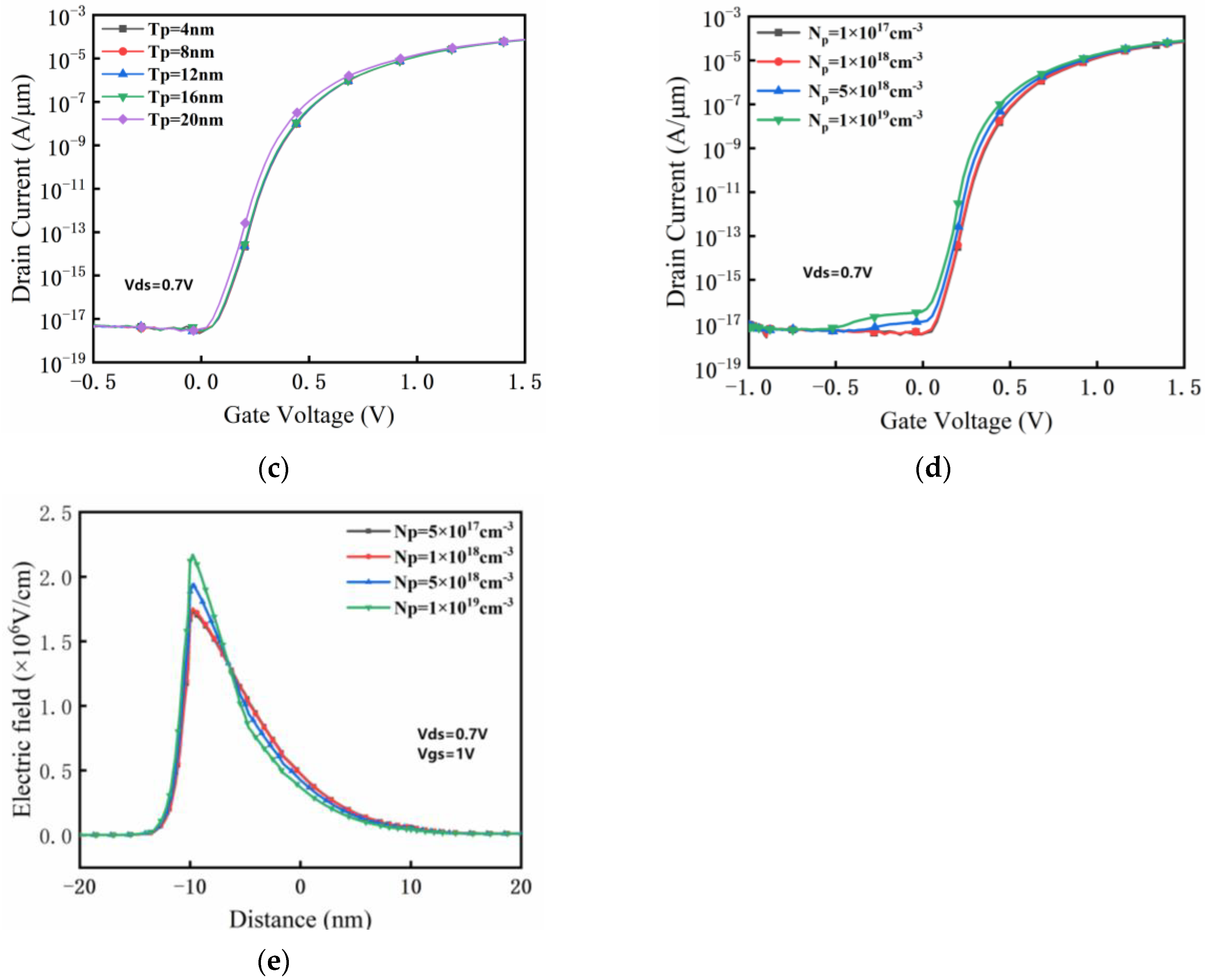
Figure 8c shows the influence of the height of the pocket (Tp) on the performance of the HJ-HD-P-DGTFET, under the condition that other parameters remain constant. It is observed that there is no significant change in Ion when the TP increases from 4 nm to 16 nm, keeping the LP fixed at 2 nm. However, the Ion increases when the TP increases up to 20 nm. This is due to the fact that the higher height of the pocket results in a larger tunneling surface. That is to say, increasing height of the pocket enhances the device characteristics. Thus, 20 nm is regarded as the optimal height of the pocket.
The variations in transfer characteristics with different pocket doping concentrations (Np) are shown in Figure 8d. It is seen that higher pocket doping concentrations (Np) cause a higher off-state current. This can be attributed to electric field distribution changes with different pocket doping concentrations, as shown in Figure 8e. The electric field in the source/channel interface (−10 nm) increases with increasing Np. Consequently, the increasing electric field near the source region helps to improve the tunneling probability in this region. Therefore, 1 × 1018 cm−3 is regarded as the optimal Np.

3.5. Comparison of Analog/RF Performance

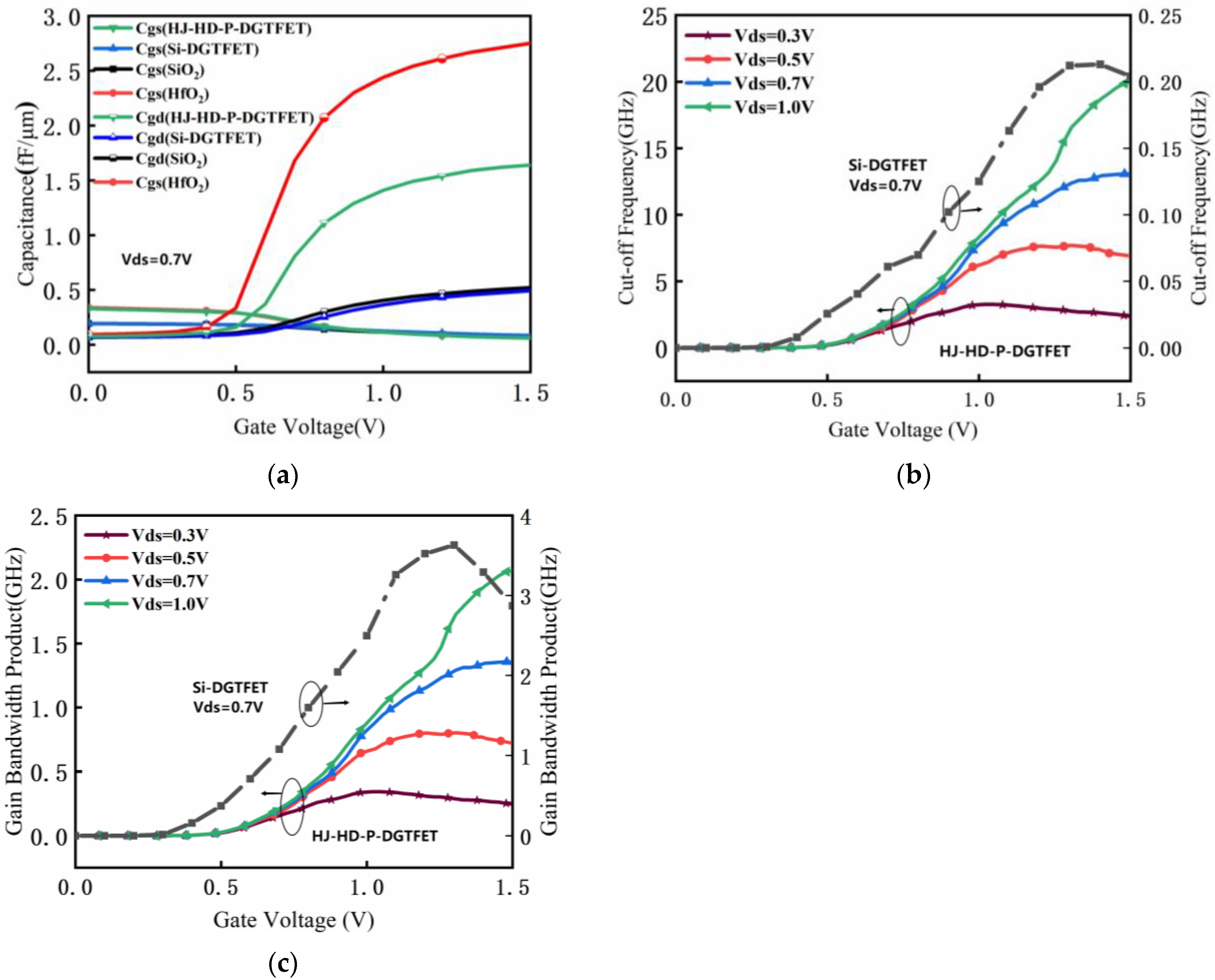
Figure 9a shows a comparison of Cgd and Cgs of the four devices at a frequency of 1.0 × 10⁶ Hz. There is not much difference in Cgs for the four studied TFETs, as shown in Figure 9a. Moreover, it is very clear that both Cgg and Cgd of HJ-P-DGTFET Hk (single gate dielectric material is HfO2, and other parameters are the same as HJ-HD-P-DGTFET) and HJ-HD-P-DGTFET increase rapidly with increasing Vgs, while the Cgg and Cgd of HJ-P-DGTFET Lk (single gate dielectric material is SiO2, and other parameters are the same as HJ-HD-P-DGTFET) and Si-DGTFET (parameters are referred to in Table 1) maintain a very small value. Although the gate capacitance characteristics of HJ-HD-P-DGTFET are poor, capacitance is only one aspect that must be considered, and transconductance and Ion will also greatly affect device performance. For TFET, increasing the Ion benefits from reducing the tunneling barrier width, but this is bound to increase the capacitance. Therefore, it is necessary to comprehensively consider its DC characteristics and capacitance characteristics. In fact, the large leakage capacitance of the TFET is attributed to its intrinsic capacitance, which is also related to the conduction mechanism. It is difficult to reduce the gate leakage intrinsic capacitance of the TFET, owing to the fact that the gate leakage intrinsic capacitance affects the tunneling current of the device. Therefore, solving the TFET gate leakage capacitance is still a challenging task.
In the design of RF applications, the parameters of cut-off frequency (fT) and gain-bandwidth product (GWB) are figures of merit (FOMs). Figure 9b,c show the cut-off frequency and gain-bandwidth product calculated by Equations (1) and (2). The results show that the fT first increases with Vgs due to an increased gm value. However, it subsequently decreases with Vgs due to the increase in Cgd and the reduction in gm. The decrease in gm can be attributed to the degradation of mobility with the gate field. It is found that the maximum fT of HJ-HD-P-DGTFET is 19.95 GHz, which is greater than the fT of the Si-DGTFET (0.22 GHz). This makes HJ-HD-P-DGTFET more suitable for RF applications.
f T = g m 2 π ( C g s + C g d )
where gm represents transconductance.
GBW = g m 2 π 10 C g d
As shown in Figure 9c, it is observed that a higher GWB of 2.07 GHz is obtained for HJ-HD-P-DGTFET. Furthermore, it is noted that the GWB initially increases with Vgs because of the increase in transconductance (gm), then decreases as Vgs continues to rise, resulting from an increase in Cgd and a decrease in gm. Comparing the two devices, the GBW of the HJ-HD-P-DGTFET is less than that of the Si-DGTFET.

3.6. Comparison of Different TFETs with HJ-HD-P-DGTFET

In order to understand the potential of HJ-HD-P-DGTFET in ultra-low-power applications, Table 2 shows a performance comparison of different TFETs with HJ-HD-P-DGTFET. Compared to other TFETs [41,42,43,44] with different heterogeneous gate dielectric structures, HJ-HD-P-DGTFET has obvious advantages in Ion, Ioff, and Ion/Ioff ratio. This is because of the improved tunneling rate by using p-type doped SiGe material in the source region and auxiliary tunneling barrier layer (pocket) of n+-doped material between the source/channel junction. Compared to heterojunction TFETs [32,34,45,46], HJ-HD-P-DGTFET has obvious advantages in Ion/Ioff ratio and Ioff. This is due to the reduced Iamb and the increased Ion by using a low K value near the drain region and a high K value near the source region. Compared to other novel structural TFETs [47,48], HJ-HD-P-DGTFET has obvious advantages in Ioff and Ion/Ioff ratio. By combining the advantages of heterogeneous gate dielectric structures, heterojunction, and auxiliary tunneling barrier layer, HJ-HD-P-DGTFET can provide high operating current and low static power consumption in ultra-low-power applications.

4. Conclusions

In this work, a novel HJ-HD-P-DGTFET is proposed, and its electrical characteristics are simulated and analyzed. The structural characteristics, physical mechanisms, performance with different parameters, and analog/RF performance of HJ-HD-P-DGTFET are discussed and studied. Simulation results show that the new design of HJ-HD-P-DGTFET performs well in terms of both switching and analog/RF characteristics compared with the conventional Si-DGTFET. Benefitting from SiGe(source)/Si(channel) heterojunction and the heavily doped pocket within the channel, the Ion for HJ-HD-P-DGTFET is increased by nearly two orders of magnitude compared with conventional Si-DGTFET due to the increase in the tunneling rate. Owing to the use of a high-k HfO2 gate dielectric in the source region and low-k SiO2 gate dielectric in the drain region, which weakens the gate control of the channel-drain tunneling junction, the Iamb is clearly suppressed, and the Ion/Ioff ratio is greatly improved. Finally, a large Ion of 7.79 × 10⁻⁵ A/μm, a suppressed Ioff of 8.16 × 10⁻¹⁸ A/μm, Ion/Ioff of 9.55 × 10¹², SSmin of 19 mV/dec, fT of 19.95 GHz, and GBW of 2.07 GHz can be achieved by HJ-HD-P-DGTFET. Therefore, HJ-HD-P-DGTFET can be a potential candidate for future low-power IC applications.

Author Contributions

Conceptualization and writing—original draft preparation, Q.C. and R.S.; methodology and funding acquisition, Z.Q. and Q.C.; validation, R.M. and J.L.; writing—review and editing, H.L., W.H. and L.Y. All authors have read and agreed to the published version of the manuscript.

Funding

This research is financially supported by the Provincial Natural Science Foundation of Shaanxi (Grant No. 2018JQ6084) and the Key scientific research program of Shaanxi Provincial Department of Education (Grant No. 20JY061).

Data Availability Statement

Data are contained within the article.

Conflicts of Interest

We declare that we do not have any commercial or associative interest that represent a conflict of interest in connection with the submitted work.

References

  1. Allam, E.A.; Manku, T.; Ting, M.; Obrecht, M.S. Impact of technology scaling on CMOS RF devices and circuits. In Proceedings of the IEEE Custom Integrated Circuits Conference, Orlando, FL, USA, 21–24 May 2000; pp. 361–364. [Google Scholar]
  2. Millán, J.; Godignon, P.; Perpiñà, X.; Pérez-Tomás, A.; Rebollo, J. A Survey of Wide Bandgap Power Semiconductor Devices. IEEE Trans. Power Electron. 2013, 29, 2155–2163. [Google Scholar] [CrossRef]
  3. Nigam, K. Low-K Dielectric Pocket and Workfunction Engineering for DC and Analog/RF Performance Improvement in Dual Material Stack Gate Oxide Double Gate TFET. Silicon 2021, 13, 2347–2356. [Google Scholar]
  4. Mohapatra, S.K.; Pradhan, K.P.; Sahu, P.K. Effect of channel & gate engineering on Double Gate (DG) MOSFET-A comparative study. In Proceedings of the 2012 International Conference on Emerging Electronics, Mumbai, India, 15–17 December 2012; pp. 1–3. [Google Scholar]
  5. Song, J.Y.; Choi, W.Y.; Park, J.H.; Lee, J.D.; Park, B.G. Design optimization of gate-all-around (GAA) MOSFETs. IEEE Trans. Nanotechnol. 2006, 5, 186–191. [Google Scholar] [CrossRef]
  6. Liu, J.S.; Clavel, M.B.; Hudait, M.K. TBAL: Tunnel FET-Based Adiabatic Logic for Energy-Efficient, Ultra-Low Voltage IoT Applications. IEEE J. Electron Devices Soc. 2019, 7, 210–218. [Google Scholar] [CrossRef]
  7. Choi, W.Y.; Park, B.G.; Lee, J.D.; Liu, T.K. Tunneling Field-Effect Transistors (TFETs) with Subthreshold Swing (SS) Less than 60 mV/dec. IEEE Electron Device Lett. 2007, 28, 743–745. [Google Scholar] [CrossRef]
  8. Yuan, J.S.; Lin, J.; Alasad, Q.; Taheri, S. Ultra-Low-Power Design and Hardware Security Using Emerging Technologies for Internet of Things. Electronics 2017, 6, 67. [Google Scholar] [CrossRef] [Green Version]
  9. Chien, N.D.; Shih, C.H. Short channel effects in tunnel field-effect transistors with different configurations of abrupt and graded Si/SiGe heterojunctions. Superlattices Microstruct. 2016, 100, 857–866. [Google Scholar] [CrossRef]
  10. Martino, M.; Martino, J.A.; Agopian, P.; Vandooren, A.; Rooyackers, R.; Simoen, E.; Claeys, C. Analysis of current mirror circuits designed with line tunnel FET devices at different temperatures. Semicond. Sci. Technol. 2017, 32, 055015. [Google Scholar] [CrossRef] [Green Version]
  11. Zhang, M.L.; Guo, Y.F.; Zhang, J.; Yao, J.F.; Chen, J. Simulation Study of the Double-Gate Tunnel Field-Effect Transistor with Step Channel Thickness. Nanoscale Res. Lett. 2020, 15, 128. [Google Scholar] [CrossRef]
  12. Mori, T.; Fukuda, K.; Miyata, N.; Morita, Y.; Migita, S.; Mizubayashi, W.; Masahara, M.; Yasuda, T.; Ota, H. Study of gate leakage current paths in p-channel tunnel field-effect transistor by current separation measurement and device simulation. Jpn. J. Appl. Phys. 2015, 54, 8. [Google Scholar] [CrossRef]
  13. Dash, S.; Sahoo, G.; Mishra, G.P. Current switching ratio optimization using dual pocket doping engineering. Superlattices Microstruct. 2018, 113, 791–798. [Google Scholar] [CrossRef]
  14. Ferain, I.; Colinge, C.A.; Colinge, J.P. Multigate transistors as the future of classical metal-oxide-semiconductor field-effect transistors. Nature 2011, 479, 310–316. [Google Scholar] [CrossRef] [PubMed]
  15. Singh, G.; Amin, S.; Anand, S.; Sarin, R.K. Design of Si0.5Ge0.5 based tunnel field effect transistor and its performance evaluation. Superlattices Microstruct. 2016, 92, 143–156. [Google Scholar] [CrossRef]
  16. Marjani, S.; Hosseini, S.E. A novel double gate tunnel field effect transistor with 9 mV/dec average subthreshold slope. In Proceedings of the 22nd Iranian Conference on Electrical Engineering (ICEE), Tehran, Iran, 20–22 May 2014; pp. 399–402. [Google Scholar]
  17. Gopi, C.; Chauhan, S.S. Double-gate Ge, InAs-based tunnel FETs with enhanced ON-current. In Proceedings of the International Conference on Communication and Signal Processing (ICCSP), Melmaruvathur, India, 6–8 April 2016; pp. 639–641. [Google Scholar]
  18. Duan, X.L.; Zhang, J.C.; Wang, S.L.; Li, Y.; Xu, S.R.; Hao, Y. A High-Performance Gate Engineered InGaN Dopingless Tunnel FET. IEEE Trans. Electron Devices 2018, 65, 1223–1229. [Google Scholar] [CrossRef]
  19. Bashir, F.; Loan, S.A.; Rafat, M.; Alamoud, A.R.M.; Abbasi, S.A. A high performance gate engineered charge plasma based tunnel field effect transistor. J. Comput. Electron. 2015, 14, 477–485. [Google Scholar] [CrossRef]
  20. Li, C.; Guo, J.M.; Jiang, H.F.; You, H.L.; Liu, W.F.; Zhuang, Y.Q. A novel gate engineered L-shaped dopingless tunnel field-effect transistor. Appl. Phys. A 2020, 126, 412. [Google Scholar] [CrossRef]
  21. Vimala, P.; Samuel, T.S.A.; Pandian, M.K. Performance Investigation of Gate Engineered tri-Gate SOI TFETs with Different High-K Dielectric Materials for Low Power Applications. Silicon 2020, 12, 1819–1829. [Google Scholar] [CrossRef]
  22. Vanlalawmpuia, K.; Bhowmick, B. Optimization of a Hetero-Structure Vertical Tunnel FET for Enhanced Electrical Performance and Effects of Temperature Variation on RF/Linearity Parameters. Silicon 2021, 13, 155–166. [Google Scholar] [CrossRef]
  23. Choudhury, S.; Niranjan, N.K.; Baishnab, K.L.; Guha, K. Design and simulation of P-TFET for improved I-ON/I-OFF ratio and subthreshold slope using strained Si1-xGex channel heterojunction. Microsyst. Technol. 2020, 26, 1777–1782. [Google Scholar] [CrossRef]
  24. Ghosh, S.; Venkateswaran, P.; Sarkar, S.K. Analysis of circuit performance of Ge-Si hetero structure TFET based on analytical model. Circuit World 2021, 10. [Google Scholar] [CrossRef]
  25. Sant, S.; Schenk, A. Band-Offset Engineering for GeSn-SiGeSn Hetero Tunnel FETs and the Role of Strain. IEEE J. Electron Devices Soc. 2015, 3, 164–175. [Google Scholar] [CrossRef]
  26. Panda, S.; Dash, S. Drain Dielectric Pocket Engineering: Its Impact on the Electrical Performance of a Hetero-Structure Tunnel FET. Silicon 2022, 14, 9305–9317. [Google Scholar] [CrossRef]
  27. Chang, H.Y.; Adams, B.; Chien, P.Y.; Li, J.P.; Woo, J. Improved Subthreshold and Output Characteristics of Source-Pocket Si Tunnel FET by the Application of Laser Annealing. IEEE Trans. Electron Devices 2013, 60, 92–96. [Google Scholar] [CrossRef]
  28. Madan, J.; Chaujar, R. Numerical Simulation of N+ Source Pocket PIN-GAA-Tunnel FET: Impact of Interface Trap Charges and Temperature. IEEE Trans. Electron Devices 2017, 64, 1482–1488. [Google Scholar] [CrossRef]
  29. Beneventi, G.B.; Gnani, E.; Gnudi, A.; Reggiani, S.; Baccarani, G. Optimization of a Pocketed Dual-Metal-Gate TFET by Means of TCAD Simulations Accounting for Quantization-Induced Bandgap Widening. IEEE Trans. Electron Devices 2015, 62, 44–51. [Google Scholar] [CrossRef]
  30. Kumar, M.J.; Janardhanan, S. Doping-Less Tunnel Field Effect Transistor: Design and Investigation. IEEE Trans. Electron Devices 2013, 60, 3285–3290. [Google Scholar] [CrossRef] [Green Version]
  31. Vishnoi, R.; Kumar, M.J. Compact Analytical Model of Dual Material Gate Tunneling Field-Effect Transistor Using Interband Tunneling and Channel Transport. IEEE Trans. Electron Devices 2014, 61, 1936–1942. [Google Scholar] [CrossRef] [Green Version]
  32. Li, W.C.; Woo, C.S. Vertical P-TFET with a P-Type SiGe Pocket. IEEE Trans. Electron Devices 2020, 67, 1480–1484. [Google Scholar] [CrossRef]
  33. Kumar, N.; Raman, A. Design and Investigation of Charge-Plasma-Based Work Function Engineered Dual-Metal-Heterogeneous Gate Si-Si0.55Ge0.45 GAA-Cylindrical NWTFET for Ambipolar Analysis. IEEE Trans. Electron Devices 2019, 66, 1468–1474. [Google Scholar] [CrossRef]
  34. Blaeser, S.; Glass, S.; Schulte-Braucks, C.; Narimani, K.; Driesch, N.V.D.; Wirths, S.; Tiedemanm, A.T.; Trellenkamp, S.; Buca, D.; Zhao, Q.T.; et al. Novel SiGe/Si line tunneling TFET with high Ion at low VDD and constant SS. In Proceedings of the 2015 IEEE International Electron Devices Meeting (IEDM), Washington, DC, USA, 7–9 December 2015; pp. 608–611. [Google Scholar]
  35. Boucart, K.; Ionescu, A.M. Double-Gate Tunnel FET with High-k Gate Dielectric. IEEE Trans. Electron Devices 2007, 54, 1725–1733. [Google Scholar] [CrossRef]
  36. Singh, K.S.; Kumar, S.; Nigam, K. Design and Investigation of Dielectrically Modulated Dual-Material Gate-Oxide-Stack Double-Gate TFET for Label-Free Detection of Biomolecules. IEEE Trans. Electron Devices 2021, 68, 5784–5791. [Google Scholar] [CrossRef]
  37. Vimala, P.; Kumar, N. Comparative Analysis of Various Parameters of Tri-Gate MOSFET with High-K Spacer. J. Nano Res. 2019, 56, 119–130. [Google Scholar] [CrossRef]
  38. Narang, R.; Saxena, M.; Gupta, R.S.; Gupta, M. Device and Circuit Level Performance Comparison of Tunnel FET Architectures and Impact of Heterogeneous Gate Dielectric. J. Semicond. Technol. Sci. 2013, 13, 224–236. [Google Scholar] [CrossRef] [Green Version]
  39. Gandhi, Z.; Chen, N.; Singh, K. Vertical Si-Nanowire n-Type Tunneling FETs with Low Subthreshold Swing (≤50 mV/decade) at Room Temperature. IEEE Electron Device Lett. 2021, 32, 437–439. [Google Scholar] [CrossRef]
  40. Chang, L.; Choi, Y.K.; Ha, D.; Ranade, P. Extremely scaled silicon nano-CMOS devices. Proc. IEEE 2003, 91, 1860–1873. [Google Scholar] [CrossRef] [Green Version]
  41. Wu, Y.; Hasegawa, H.; Kakushima, K.; Ohmori, K.; Watanabe, T.; Nishiyama, A.; Sugii, N.; Wakabayashi, H.; Tsutsui, K.; Kataoka, Y.; et al. A novel hetero-junction Tunnel-FET using Semiconducting silicide–Silicon contact and its scalability. Microelectron. Reliab. 2014, 54, 899–904. [Google Scholar] [CrossRef]
  42. Goyal, P.; Srivastava, G.; Madan, J.; Pandey, R.; Gupta, R.S. Design and Investigation of Mg2Si Source Charge Plasma Based DGTFET for Biomolecule Detection. In Proceedings of the 2022 IEEE International Conference of Electron Devices Society Kolkata Chapter (EDKCON), Kolkata, India, 26–27 November 2022; pp. 474–478. [Google Scholar]
  43. Goyal, P.; Srivastava, G.; Madan, J.; Pandey, R.; Gupta, R.S. Source Material-Engineered Charge Plasma based Double Gate TFET for Analog/RF Applications. In Proceedings of the 2021 International Conference on Industrial Electronics Research and Applications (ICIERA), New Delhi, India, 22–24 December 2021; pp. 1–4. [Google Scholar]
  44. Babu, K.M.C.; Goel, E. Analysis of ON Current and Ambipolar Current for Source Pocket Gate-Drain Underlap Double Gate Tunnel Field Effect Transistor. In Proceedings of the 2022 IEEE International Symposium on Smart Electronic Systems (iSES), Warangal, India, 19–21 December 2022; pp. 651–653. [Google Scholar]
  45. Chen, S.; Wang, S.; Liu, H. A Novel Dopingless Fin-Shaped SiGe Channel TFET with Improved Performance. Nanoscale Res. Lett. 2020, 15, 202. [Google Scholar] [CrossRef]
  46. Kumar, N.; Amin, S.I.; Anand, S. Design and performance optimization of novel Core–Shell Dopingless GAA-nanotube TFET with Si0.5Ge0.5-based source. IEEE Trans. Electron Devices 2020, 67, 789–795. [Google Scholar]
  47. Bagga, N.; Kumar, A.; Dasgupta, S. Demonstration of a novel two source region tunnel FET. IEEE Trans. Electron Devices 2017, 64, 5256–5262. [Google Scholar] [CrossRef]
  48. Sharma, S.; Chaujar, R. High Switching Performance of Novel Heterogeneous Gate Dielectric—Hetero-Material Based Junctionless-TFET. In Microelectronics, Circuits and Systems: Select Proceedings of 7th International Conference on Micro2020; Springer: Singapore, 2021; pp. 3–12. [Google Scholar]
Figure 1. Schematic diagram of (a) HJ-HD-P-DGTFET; (b) Si-DGTFET.
Micromachines 14 00784 g001
Figure 2. Model calibration against the work from Narang R et al. [38]. The inset shows the transmission characteristics of the HJ-HD-P-DGTFET.
Micromachines 14 00784 g002
Figure 3. Fabrication process of the HJ-HD-P-DGTFET. (a) Silicon substrate preparation and the n+ region is introduced, after which a n+ pocket is deposited by epitaxy. Subsequently, the source region is implanted; (b) etching is performed in the channel region, and isolation oxide is deposited; (c) oxidation growth of SiO2; (d) SiO2 gate dielectric is selectively etched away at the source side; (e) the HfO2 is deposited by ALD; (f) gate deposition, silicon exposure, etc.
Micromachines 14 00784 g003
Figure 4. (a) Transfer characteristics (b) on-state energy band of HJ-HD-P-DGTFET and Si-DGTFET.
Micromachines 14 00784 g004
Figure 5. (a) The transfer characteristics; (b) on-state energy band diagram of HJ-HD-P-DGTFET with different SiGe composition rates.
Micromachines 14 00784 g005
Figure 6. The influence of Ns on (a) transfer characteristics; (b) the on-state energy band diagram; (c) the distribution of the electric field.
Micromachines 14 00784 g006
Figure 7. Transfer characteristics of HJ-HD-P-DGTFET with (a) different gate dielectric materials; (b) different gate dielectric thicknesses To; (c) the distribution of electric field with different gate dielectric thicknesses To; (d) transfer characteristics of HJ-HD-P-DGTFET with different gate work function ΦM.
Micromachines 14 00784 g007
Figure 8. (a) Transfer characteristics of HJ-HD-P-DGTFET with different Lp; (b) the distribution of BTBT tunneling rate with different Lp; (c) transfer characteristics of HJ-HD-P-DGTFET with different Tp; (d) transfer characteristics of HJ-HD-P-DGTFET with different Np; (e) the distribution of electric field with different Np.
Micromachines 14 00784 g008aMicromachines 14 00784 g008b
Figure 9. (a) Capacitance voltage characteristics of the HJ-HD-P-DGTFET and Si-DGTFET; (b) cut-off frequency (fT) and (c) the gain bandwidth (GBW) plots of both HJ-HD-P-DGTFET and Si-DGTFET.
Micromachines 14 00784 g009
Table 1. Various structural specification parameters of the presented TFETs for the simulation.
ParametersHJ-HD-P-DGTFETSi-DGTFET
Source doping (p-type)1 × 1020 cm−31 × 1020 cm−3
Drain doping (n-type)1 × 1018 cm−31 × 1018 cm−3
Channel doping (p-type)1 × 1016 cm−31 × 1016 cm−3
Pocket doping (n-type)1 × 1018 cm−3
Gate oxide thickness (To)2 nm2 nm
Pocket length (Lp)2 nm
Gate dielectric constant of SiO2 (ε)3.93.9
Gate dielectric constant of HfO2 (ε)25
Gate work function (Φm)4.3 eV4.3 eV
Table 2. Performance comparison of different TFETs with HJ-HD-P-DGTFET.
DeviceIon (A/μm)Ioff (A/μm)Ion/Ioff Ratio
CP-DGTFET [41]5.8 × 10−710−15108
SP-GDU-DGTFET [42]10−710−171010
DF-TFET [43]3.8 × 10−62.7 × 10−171011
DS-TFET [44]1.0 × 10−81.9 × 10−16107
Mg2Si source CP-DGTFET [45]4.6 × 10−310−161013
Ge CP-DGTFET [32]10−610−181012
Si0.8Ge0.2 pocket TFET [34]10−610−13107
SiGe/Si TFET [46]6.7 × 10−62.0 × 10−10104
CS-DL-NT-TFET [47]1.7 × 10−52.0 × 10−171011
HD-HJLTFET [48]4.5 × 10−51.5 × 10−161011
This work7.8 × 10−58.2 × 10−181012
Disclaimer/Publisher’s Note: The statements, opinions and data contained in all publications are solely those of the individual author(s) and contributor(s) and not of MDPI and/or the editor(s). MDPI and/or the editor(s) disclaim responsibility for any injury to people or property resulting from any ideas, methods, instructions or products referred to in the content.