
Femtosecond Laser Processing Assisted SiC High-Temperature Pressure Sensor Fabrication and Performance Test


Abstract
:1. Introduction
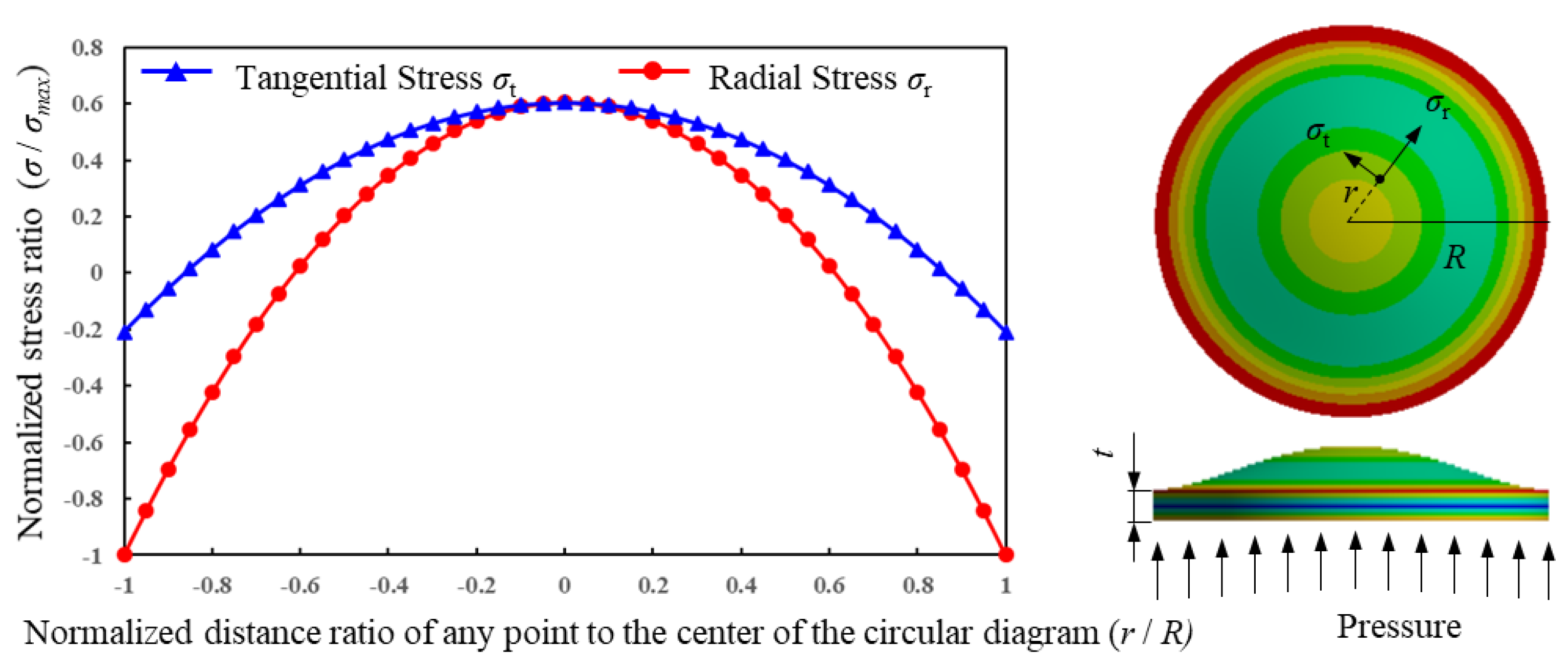
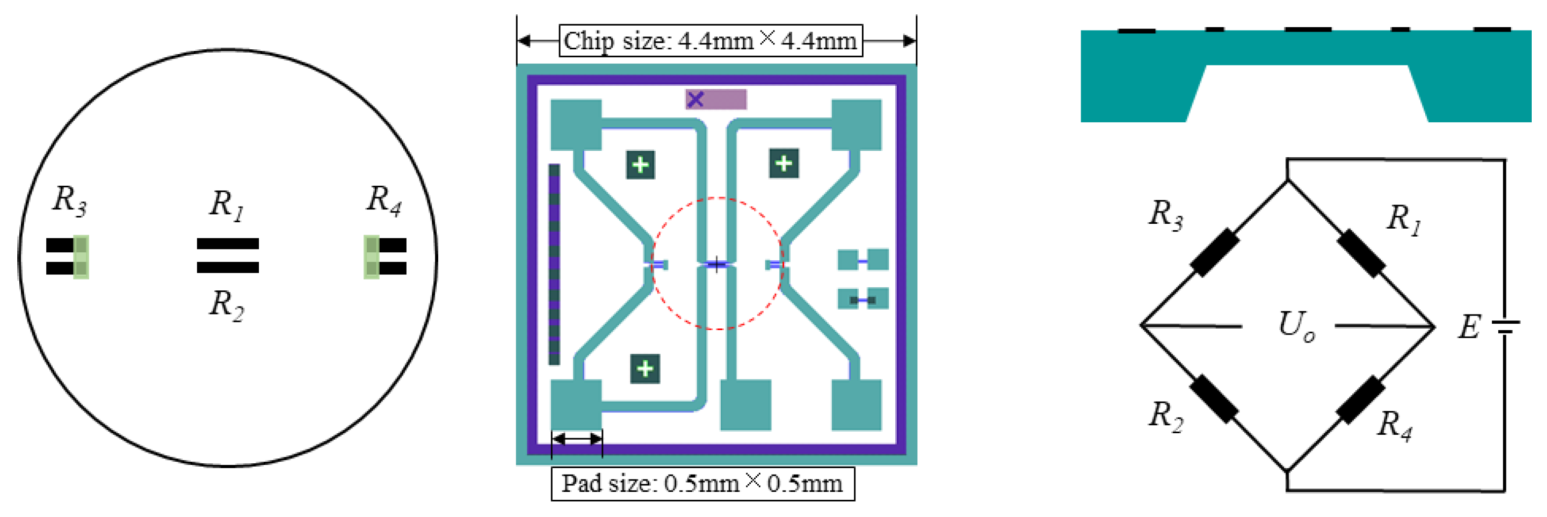
2. Sensor Design
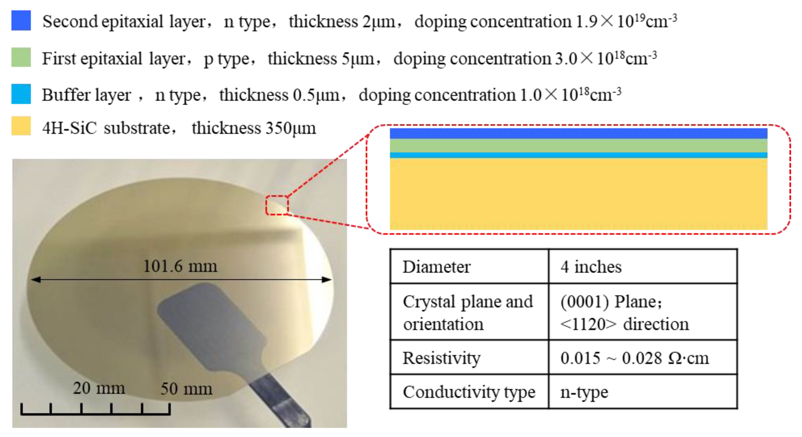
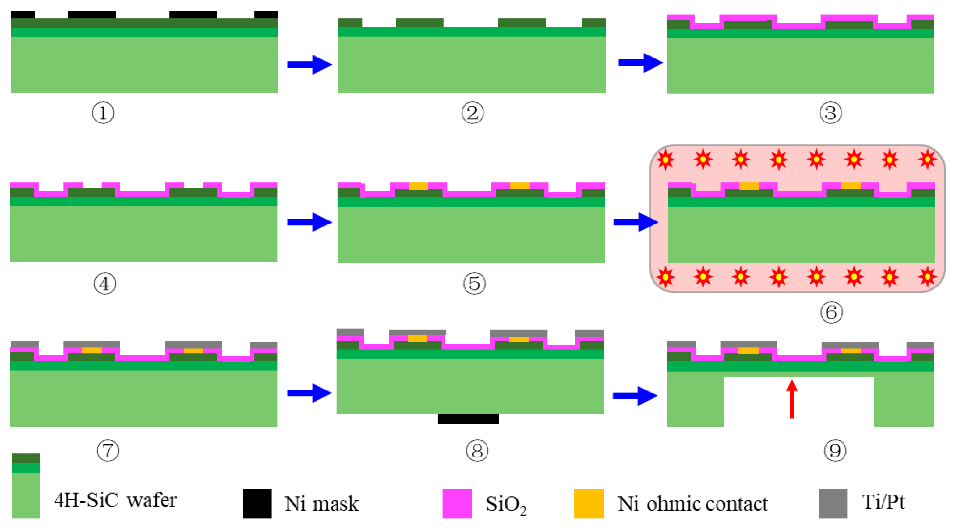
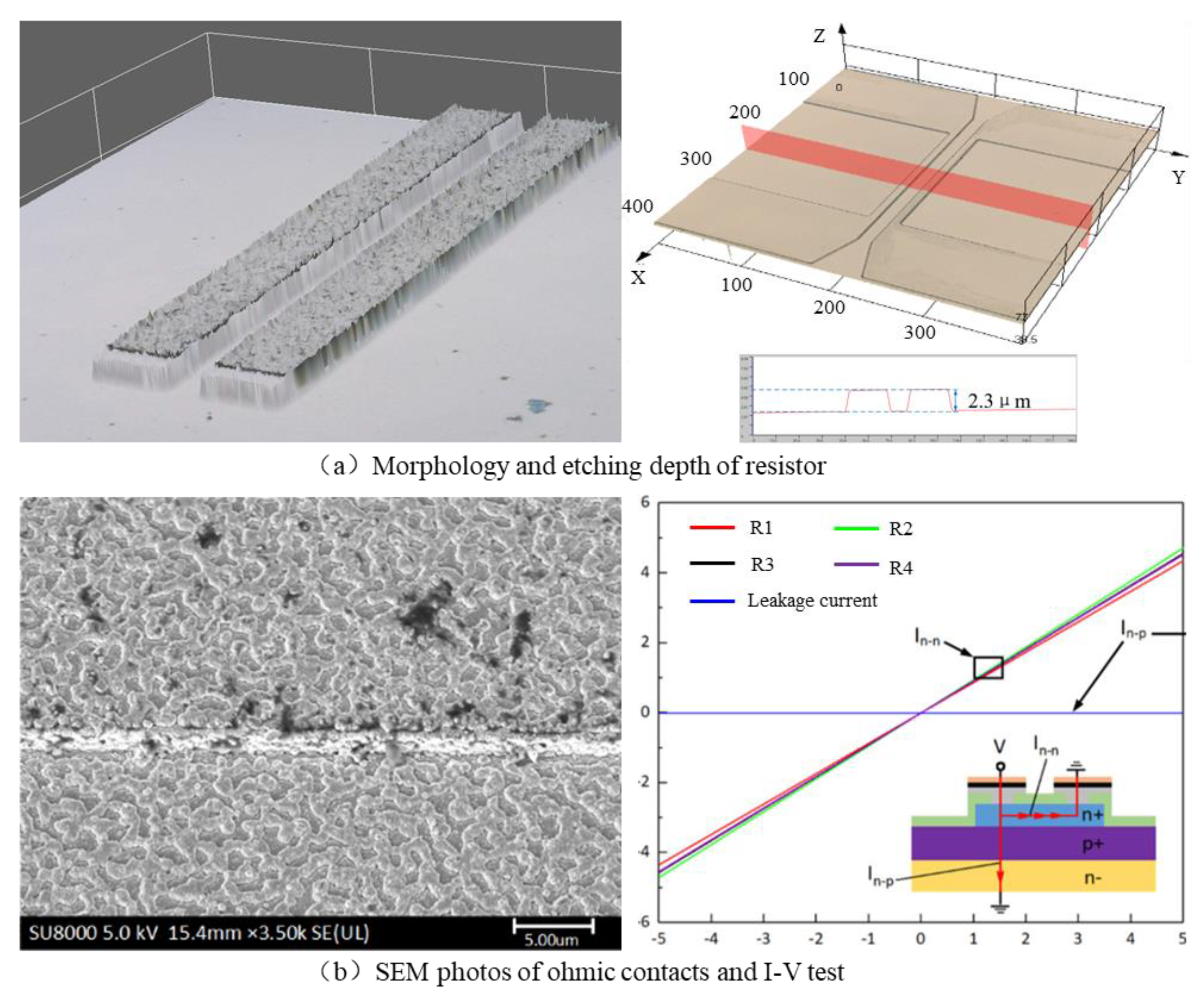
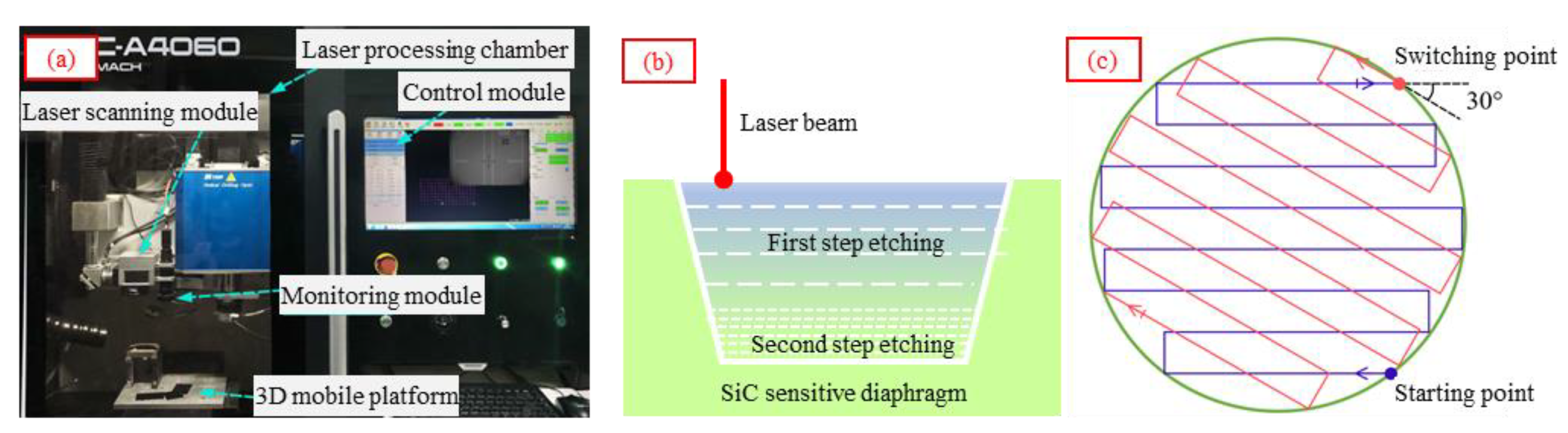
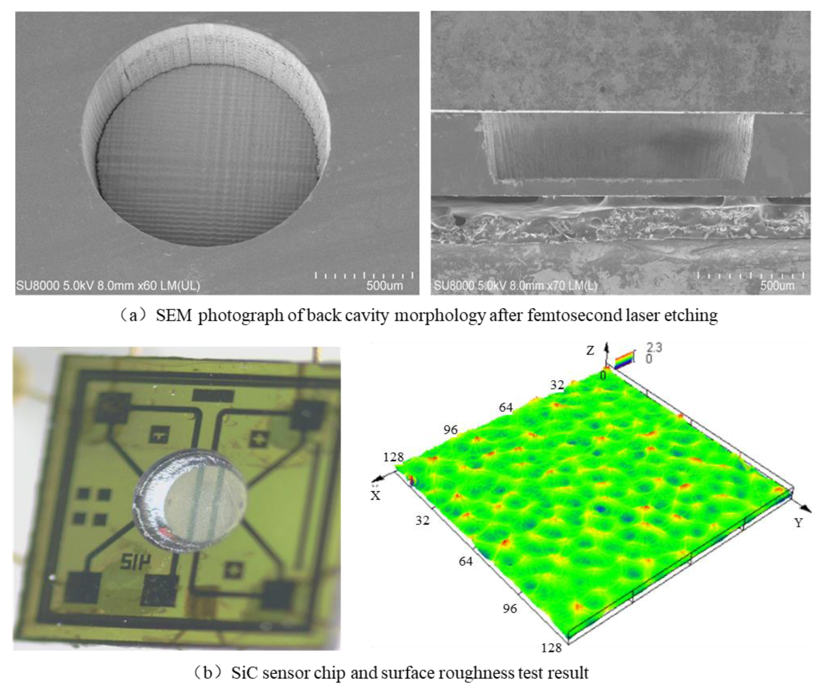
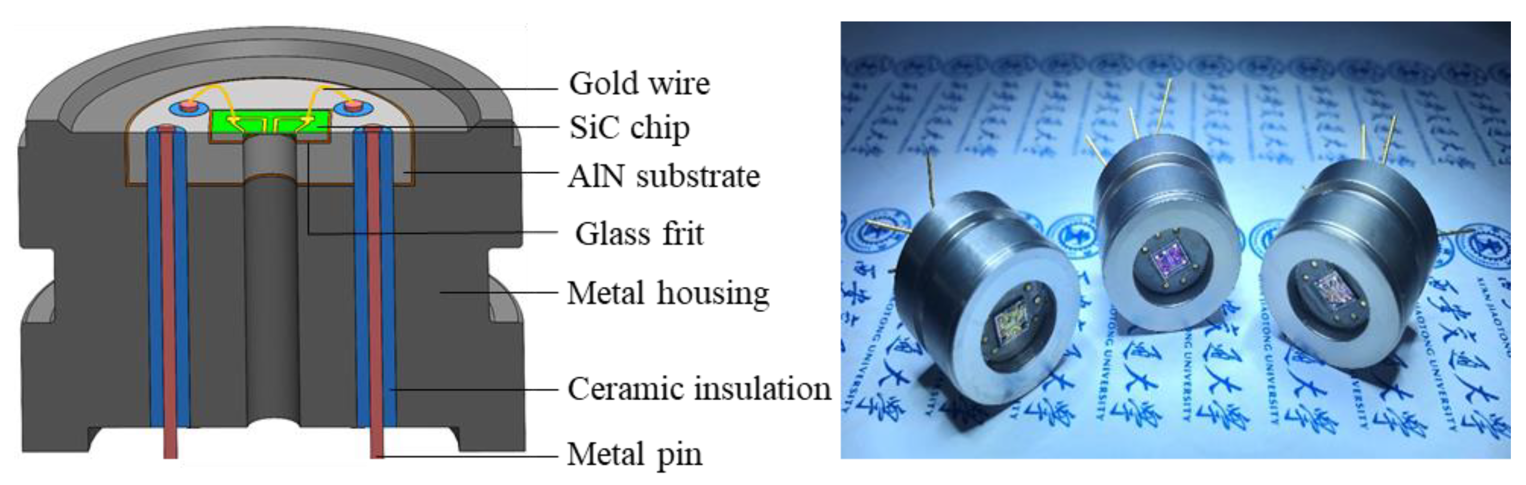
3. Sensor Fabrication
4. Results and Discussion
4.1. Static Calibration
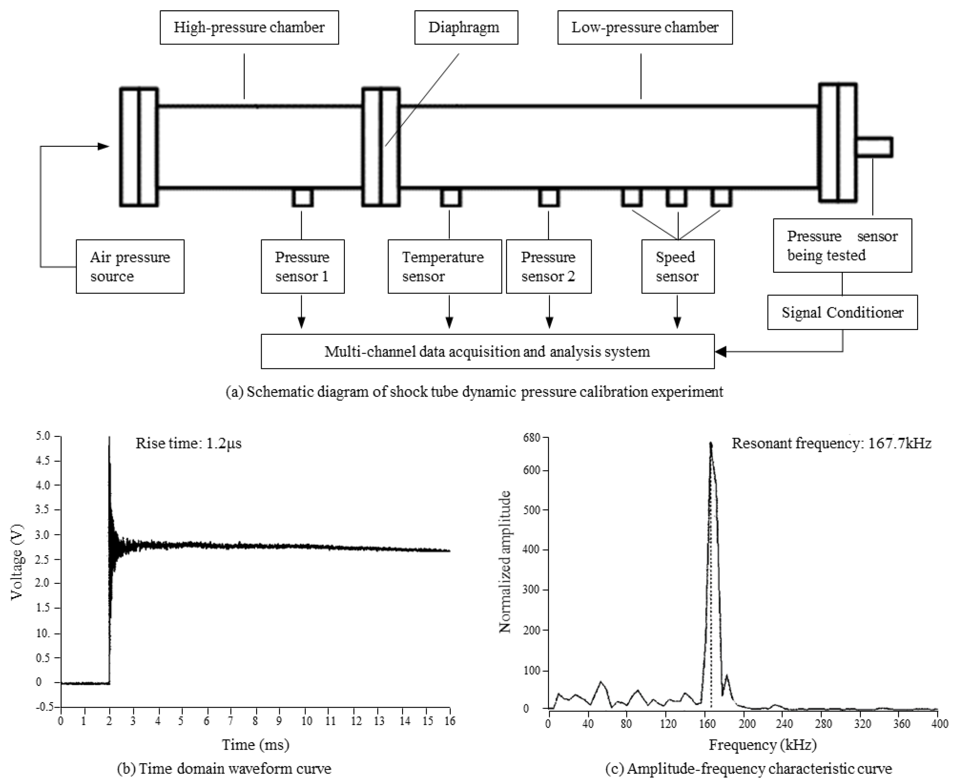
4.2. Dynamic Calibration
4.3. High Temperature Performance Test
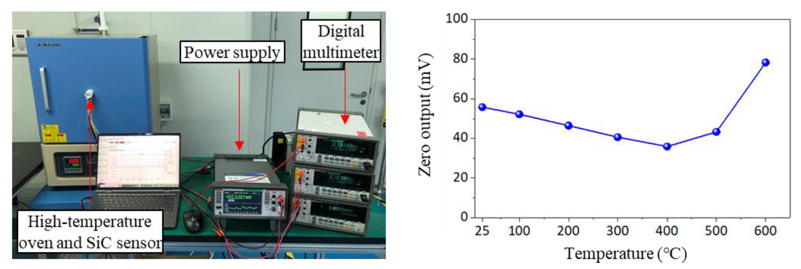
4.3.1. Thermal Zero Offset Drift
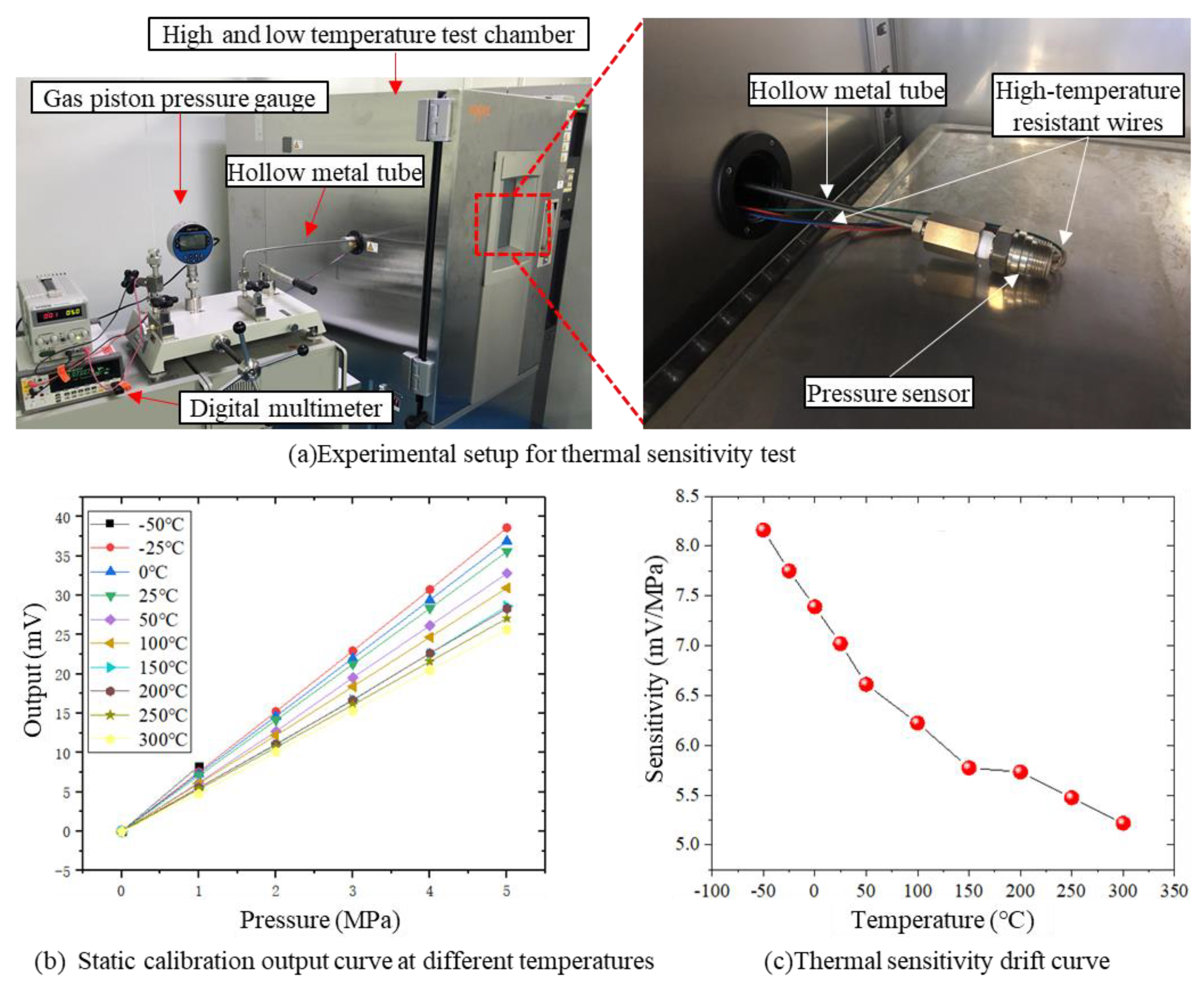
4.3.2. High and Low Temperature Calibration
5. Conclusions
Author Contributions
Funding
Data Availability Statement
Conflicts of Interest
References
- Griffin, B.A.; Habermehl, S.D.; Clews, P.J. Development of an Aluminum Nitride-Silicon Carbide Material Set for High Temperature Sensor Applications. In Proceedings of the Conference on Sensors for Extreme Harsh Environments, Baltimore, MD, USA, 5 May 2014. [Google Scholar]
- Zhang, Z.; Wang, Y.; Zhou, M.; He, J.; Liao, C.; Wang, Y. Recent advance in hollow-core fiber high-temperature and high-pressure sensing technology. Chin. Opt. Lett. 2021, 19, 15. [Google Scholar] [CrossRef]
- Li, B.; Zhang, H.Y.; Yang, J.; Zhang, Z.J. Dynamic Measurement Device of Aeroengine Pressure Probe. In Proceedings of the 4th International Conference on Aeronautical, Aerospace and Mechanical Engineering (AAME) 2021, Sanya, China, 26–28 February 2021. [Google Scholar]
- Scardelletti, M.A.; Zorman, C.A. Packaged Capacitive Pressure Sensor System for Aircraft Engine Health Monitoring. In Proceedings of the 15th IEEE Sensors Conference, Orlando, FL, USA, 30 October–2 November 2016. [Google Scholar]
- Middelburg, L.M.; Drie, W.D.; Zhang, G.Q. From Si Towards SiC Technology for Harsh Environment Sensing. In Sensor Systems Simulations: From Concept to Solution; Springer International Publishing: Berlin, Germany, 2020; pp. 7–9. [Google Scholar]
- Lu, C.; Li, X.Y.; Yao, Y.L.; Tang, X.L.; Peng, Y.; Wang, S.F. Design and Implementation of Parallel Prediction Model for Aeroengine Multi-Sensor. J. Univ. Electron. Sci. Technol. China 2021, 50, 580–585. [Google Scholar]
- Seo, Y.; Kim, D.; Hall, N.A. High-Temperature Piezoelectric Pressure Sensors for Hypersonic Flow Measurements. In Proceedings of the International Conference on Solid-State Sensors, Actuators and Microsystems & Eurosensors XXXIII, Berlin, Germany, 23–27 June 2019. [Google Scholar]
- Seo, Y.; Kim, D.; Hall, N.A. On-Diaphragm Thermistor for High-Temperature Dynamic Pressure Sensors. IEEE Sens. J. 2019, 20, 2287–2293. [Google Scholar] [CrossRef]
- Kim, N.I.; Chang, Y.L.; Chen, J.; Barbee, T.; Wang, W.; Kim, J.Y.; Kwon, M.-K.; Shervin, S.; Moradnia, M.; Pouladi, S.; et al. Piezoelectric pressure sensor based on flexible gallium nitride thin film for harsh-environment and high-temperature applications. Sens. Actuators A Phys. 2020, 305, 111940. [Google Scholar] [CrossRef]
- PCB Piezotronics. Product Finder [EB/OL]. Available online: https://www.pcb.com/products?m=176A03 (accessed on 22 July 2022).
- Lv, H.; Lai, K.; Qi, Y. Analysis of a micro pressure-sensor employing SiC-AlN-SiC structure. Aust. J. Mech. Eng. 2022, 20, 194–200. [Google Scholar] [CrossRef]
- Mikhailov, P.G.; Ualiyev, Z.; Kabdoldina, A. Issues of Development of Capacitive Pressure Sensors Operable under Extreme Operating Conditions. In Proceedings of the 2020 International Russian Automation Conference (RusAutoCon), Sochi, Russia, 6–12 September 2020. [Google Scholar]
- Li, C.; Jia, P.; Sun, B.; Hong, Y.; Xue, Y.; Jia, M.; Xiong, J. A Differential Split-Type Pressure Sensor for High-Temperature Applications. IEEE Access 2021, 9, 20641–20647. [Google Scholar] [CrossRef]
- Li, C.; Sun, B.; Jia, P.; Xue, Y.; Jia, M.; Xiong, J. Capacitive Pressure Sensor With Integrated Signal-Conversion Circuit for High-Temperature Applications. IEEE Access 2020, 8, 212787–212793. [Google Scholar] [CrossRef]
- Wang, S.; Wang, J.; Li, W.; Liu, Y.; Li, J.; Jia, P. A MEMS-Based High-Fineness Fiber-Optic Fabry-Perot Pressure Sensor for High-Temperature Application. Micromachines 2022, 13, 763. [Google Scholar] [CrossRef]
- Chen, X.; Tong, X.; Zhang, C.; Deng, C.; Mao, Y.; Chen, S. High-precision optical fiber Fabry–Perot composite sensor for pressure and temperature. Opt. Commun. 2022, 506, 127580. [Google Scholar] [CrossRef]
- Feng, F.; Jia, P.; Qian, J.; Hu, Z.; An, G.; Qin, L. High-Consistency Optical Fiber Fabry–Perot Pressure Sensor Based on Silicon MEMS Technology for High Temperature Environment. Micromachines 2021, 12, 623. [Google Scholar] [CrossRef]
- Reja, M.I.; Nguyen, L.V.; Peng, L.; Ebendorff-Heidepriem, H.; Warren-Smith, S.C. Temperature-Compensated Interferometric High-Temperature Pressure Sensor Using a Pure Silica Microstructured Optical Fiber. IEEE Trans. Instrum. Meas. 2022, 71, 7002612. [Google Scholar] [CrossRef]
- Ngo, H.D.; Ehrmann, O.; Schneider-Ramelow, M.; Lang, K.D. Piezoresistive Pressure Sensors for Applications in Harsh Environments—A Roadmap. Smart Sens. Meas. Instrum. 2019, 29, 231–251. [Google Scholar]
- Moser, M.; Pradhan, M.; Alomari, M.; Burghartz, J.N. Model and Simulation of GaN-Based Pressure Sensors for High Temperature Applications—Part II: Sensor Design and Simulation. IEEE Sens. J. 2021, 21, 20176–20183. [Google Scholar] [CrossRef]
- Endevco Corporation. Test & Measurement Sensor Catalog [EB/OL]. Available online: http://endevco.com/contentStore/MktgContent/Endevco/uploads/2019/08/EDV-Catalog_Lowres.pdf (accessed on 22 July 2022).
- Tang, X.; Tian, J.; Zhao, J.; Jin, Z.; Liu, Y.; Liu, J.; Chen, T.; Li, J. SOI Structure design and optimization of SOI high-temperature pressure sensor chip. Microelectron. J. 2021, 118, 105245. [Google Scholar] [CrossRef]
- Okojie, R.S.; Howard, R.T.; Richards, R.D. Stable 600 °C silicon carbide MEMS pressure transducers. In Proceedings of the Conference on Sensors and Systems for Space Applications, Orlando, FL, USA, 9–11 April 2007. [Google Scholar]
- Okojie, R.S.; Lukco, D.; Nguyen, V.; Savrun, E. Demonstration of SiC Pressure Sensors at 750 °C. In Proceedings of the IMAPS International Conference and Exhibition on High Temperature Electronics, HiTEC 2014, Albuquerque, NM, USA, 13–15 May 2014. [Google Scholar]
- Shang, H.; Tian, B.; Wang, D.; Liu, Y.; Wang, W. Development of All-SiC Absolute Pressure Sensor Based on Sealed Cavity Structure. IEEE Sens. J. 2021, 21, 27308–27314. [Google Scholar] [CrossRef]
- Tian, B.H.; Shang, H.P.; Wang, W.B. Research on Temperature Zero Drift of SiC Piezoresistive Pressure Sensor Based on Asymmetric Wheatstone Bridge. Silicon 2022, 14, 5445–5451. [Google Scholar] [CrossRef]
- Tian, B.; Shang, H.; Wang, D.; Liu, Y.; Wang, W. Investigation on Piezoresistive Effect of n-Type 4H-SiC Based on All-SiC Pressure Sensors. IEEE Sens. J. 2022, 22, 6435–6441. [Google Scholar] [CrossRef]
- Li, Y.; Liang, T.; Lei, C.; Li, Q.; Li, Z.; Ghaffar, A.; Xiong, J. Study on the Stability of the Electrical Connection of High-Temperature Pressure Sensor Based on the Piezoresistive Effect of P-Type SiC. Micromachines 2021, 12, 216. [Google Scholar] [CrossRef] [PubMed]
- Akiyama, T.; Briand, D.; Rooij, N.D. Design-dependent gauge factors of highly doped n-type 4H-SiC piezoresistors. J. Micromechanics Microengineering 2012, 22, 085034. [Google Scholar] [CrossRef]
- Marsi, N.; Majlis, B.Y.; Hamzah, A.A.; Mohd-Yasin, F. Development of high temperature resistant of 500 °C employing silicon carbide (3C-SiC) based MEMS pressure sensor. Microsyst. Technol. 2015, 21, 319–330. [Google Scholar] [CrossRef]
- He, H.T.; Wang, W.Z.; Du, S.B.; Hu, L.Y.; Yang, Z. A Novel MEMS Piezoresistivity SiC High Temperature Pressure Sensor. Micronanoelectronic. Technol. 2015, 52, 233–239. [Google Scholar]
- Okojie, R.S.; Ned, A.A.; Kurtz, A.D. Operation of α(6H-) SiC pressure sensor at 500 °C. Sens. Actuators A Phys. 1998, 66, 200–204. [Google Scholar] [CrossRef]
- Okojie, R.S.; Blaha, C.; Lukco, D.; Nguyen, V.; Savrun, E. Zero offset drift suppression in SiC pressure sensors at 600 °C. In Proceedings of the IEEE Sensors 2010, Waikoloa, HI, USA, 1–4 November 2010; pp. 2269–2274. [Google Scholar]
- Okojie, R.S.; Lukco, D.; Nguyen, V.; Savrun, E. 4H-SiC piezoresistive pressure sensors at 800 °C with observed sensitivity recovery. IEEE Electron Device Lett. 2015, 36, 174–176. [Google Scholar] [CrossRef]


| Parameters | First Step Etching | Second Step Etching |
|---|---|---|
| Laser wavelength | 1030 nm | |
| Repetition frequency | 100 kHz | |
| Pulse width | 240 fs | |
| Laser delay | 150 μs | |
| Laser off delay | 120 μs | |
| Poly delay | 5 μs | |
| End delay | 5 μs | |
| Laser power | 5 W | 4.2 W |
| Number of scans | 3000 | 1200 |
| Scanning speed | 2500 mm/s | 3000 mm/s |
| Scanline spacing | 10 μm | 5 μm |
| Etching depth | 200 μm | 50~70 μm |
| Pressure | 1st Calibration | 2nd Calibration | 3rd Calibration | 4th Calibration | 5th Calibration |
|---|---|---|---|---|---|
| 0 MPa | −0.01 mV | −0.01 mV | −0.02 mV | −0.02 mV | −0.03 mV |
| 1 MPa | 9.33 mV | 9.32 mV | 9.32 mV | 9.31 mV | 9.30 mV |
| 2 MPa | 18.92 mV | 18.91 mV | 18.90 mV | 18.89 mV | 18.89 mV |
| 3 MPa | 28.76 mV | 28.76 mV | 28.74 mV | 28.73 mV | 28.72 mV |
| 4 MPa | 38.87 mV | 38.86 mV | 38.85 mV | 38.84 mV | 38.83 mV |
| 5 MPa | 49.26 mV | 49.24 mV | 49.23 mV | 49.22 mV | 49.21 mV |
| Reference | Repeatability Error | Hysteresis Error | Linearity Error |
|---|---|---|---|
| This paper | 0.10%FS | 0.11%FS | 1.01%FS |
| [25] | 0.23%FS | 0.17%FS | 0.03%FS |
| [30] | / | ≤0.1%FS | 0.49%FS |
| [31] | / | / | 1.05%FS |
| [32] | / | 0.17%FS | 0.17%FS |
| t (°C) | 100 | 200 | 300 | 400 | 500 | 600 |
|---|---|---|---|---|---|---|
| TCO | 0.01% | 0.03% | 0.04% | 0.06% | 0.02% | 0.04% |
Disclaimer/Publisher’s Note: The statements, opinions and data contained in all publications are solely those of the individual author(s) and contributor(s) and not of MDPI and/or the editor(s). MDPI and/or the editor(s) disclaim responsibility for any injury to people or property resulting from any ideas, methods, instructions or products referred to in the content. |
© 2023 by the authors. Licensee MDPI, Basel, Switzerland. This article is an open access article distributed under the terms and conditions of the Creative Commons Attribution (CC BY) license (https://creativecommons.org/licenses/by/4.0/).
Share and Cite
Zhao, Y.; Zhao, Y.; Wang, L.; Yang, Y.; Wang, Y. Femtosecond Laser Processing Assisted SiC High-Temperature Pressure Sensor Fabrication and Performance Test. Micromachines 2023, 14, 587. https://doi.org/10.3390/mi14030587
Zhao Y, Zhao Y, Wang L, Yang Y, Wang Y. Femtosecond Laser Processing Assisted SiC High-Temperature Pressure Sensor Fabrication and Performance Test. Micromachines. 2023; 14(3):587. https://doi.org/10.3390/mi14030587
Chicago/Turabian StyleZhao, You, Yulong Zhao, Lukang Wang, Yu Yang, and Yabing Wang. 2023. "Femtosecond Laser Processing Assisted SiC High-Temperature Pressure Sensor Fabrication and Performance Test" Micromachines 14, no. 3: 587. https://doi.org/10.3390/mi14030587
APA StyleZhao, Y., Zhao, Y., Wang, L., Yang, Y., & Wang, Y. (2023). Femtosecond Laser Processing Assisted SiC High-Temperature Pressure Sensor Fabrication and Performance Test. Micromachines, 14(3), 587. https://doi.org/10.3390/mi14030587