


A Novel Super-Junction DT-MOS with Floating p Regions to Improve Short-Circuit Ruggedness


Abstract
:1. Introduction
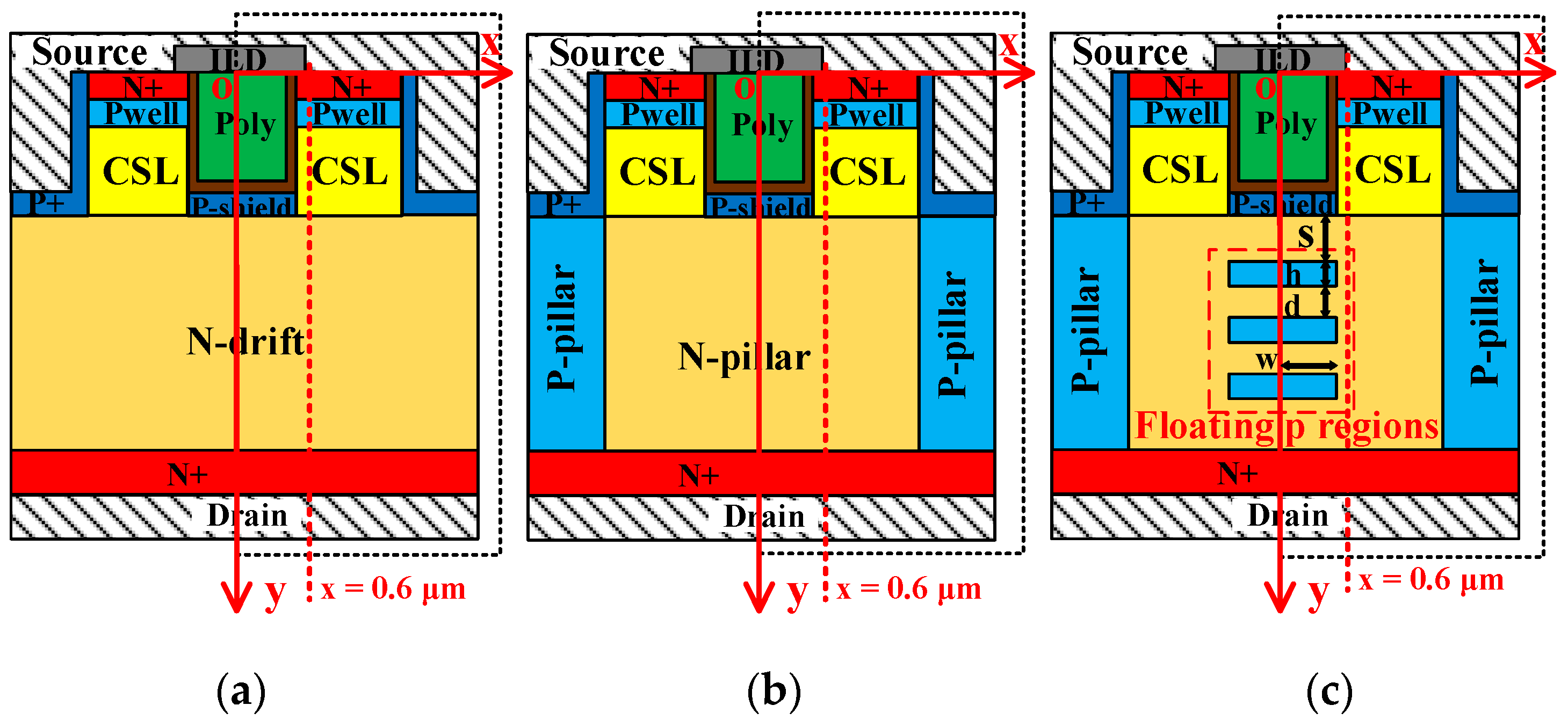
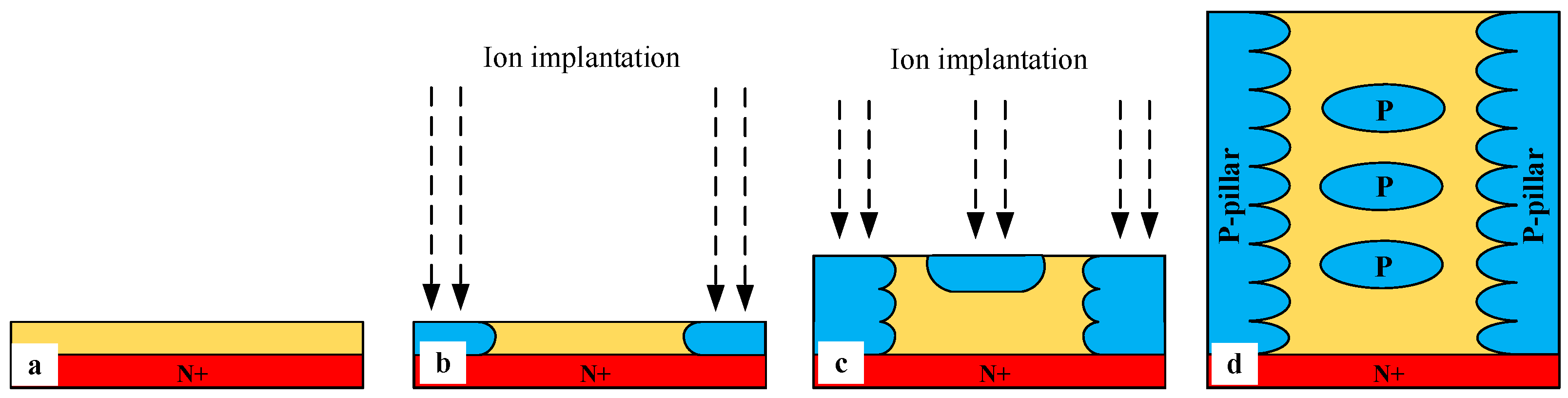
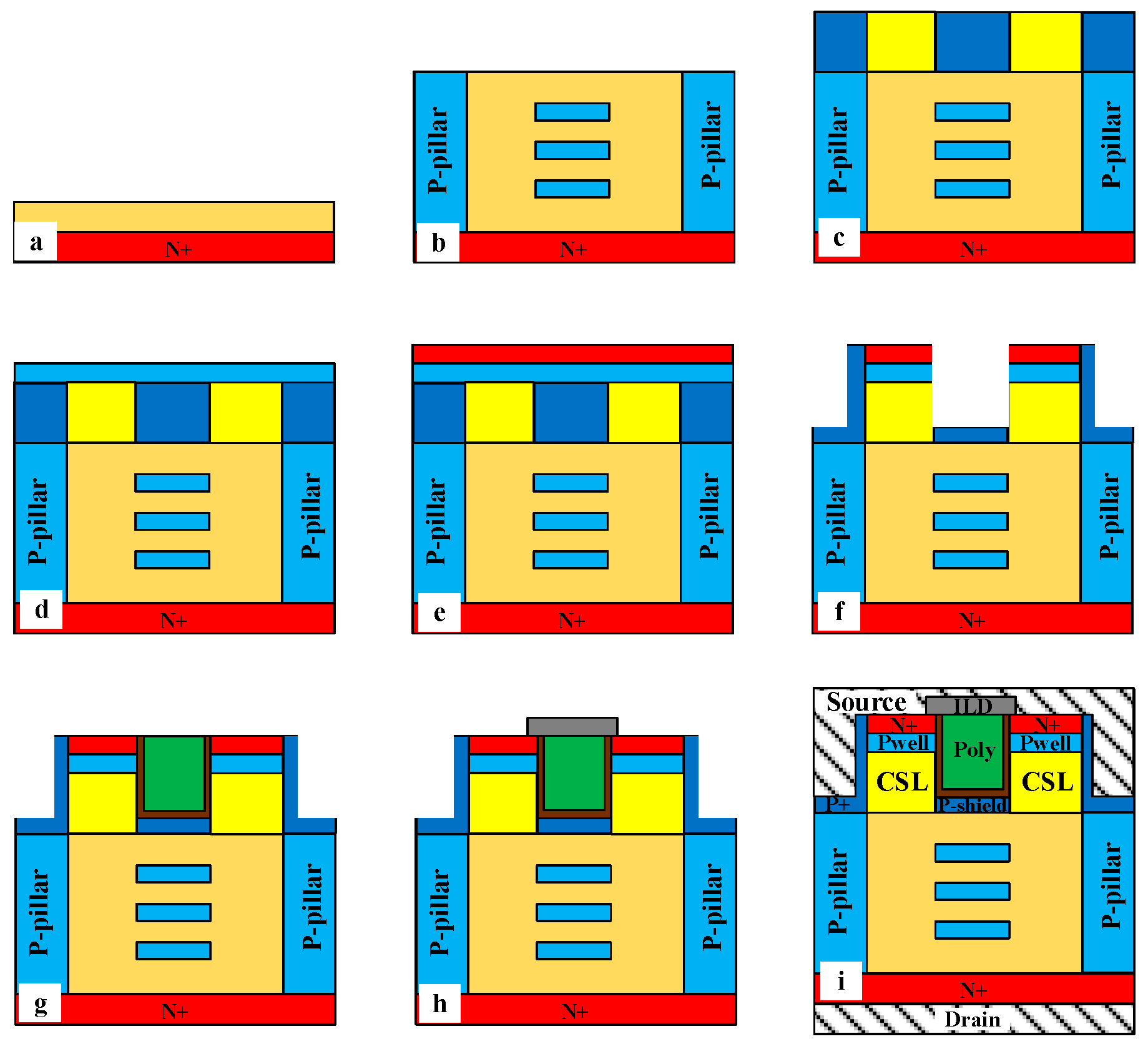
2. Device Structure
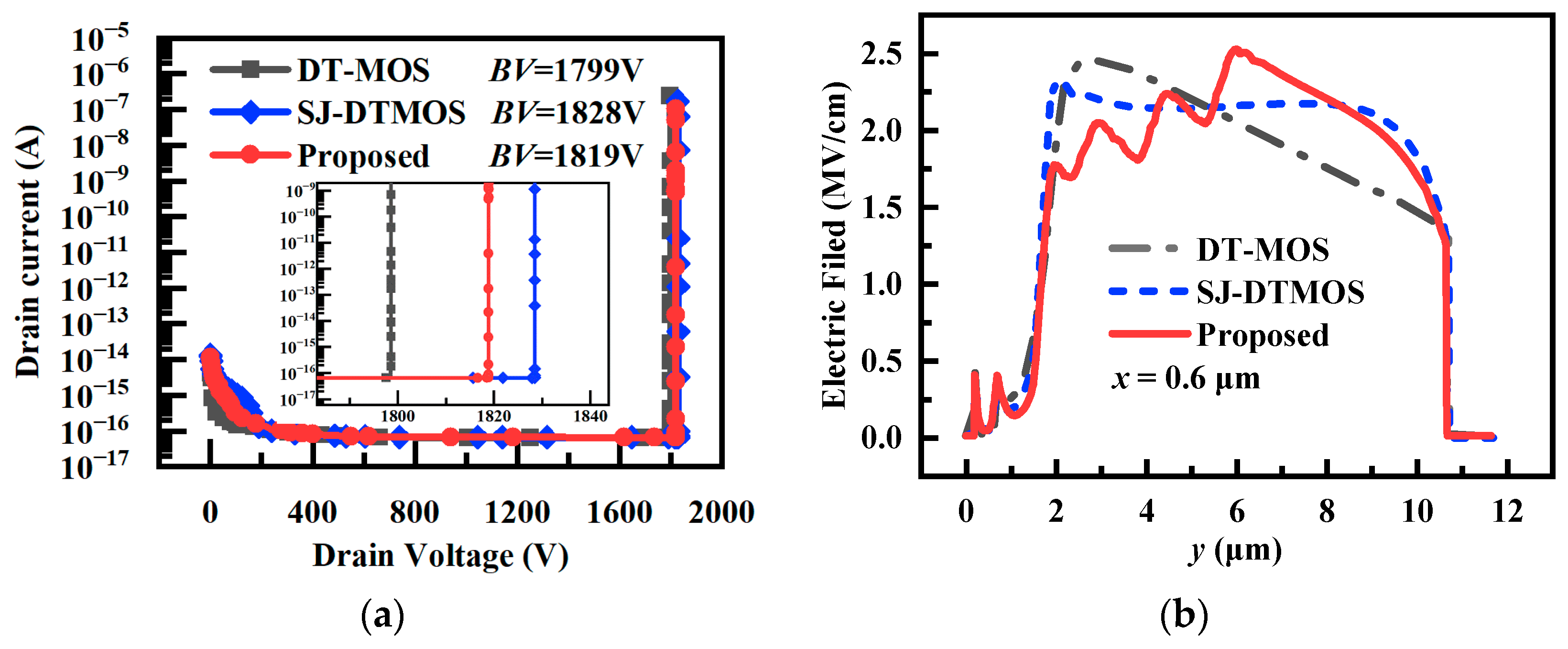
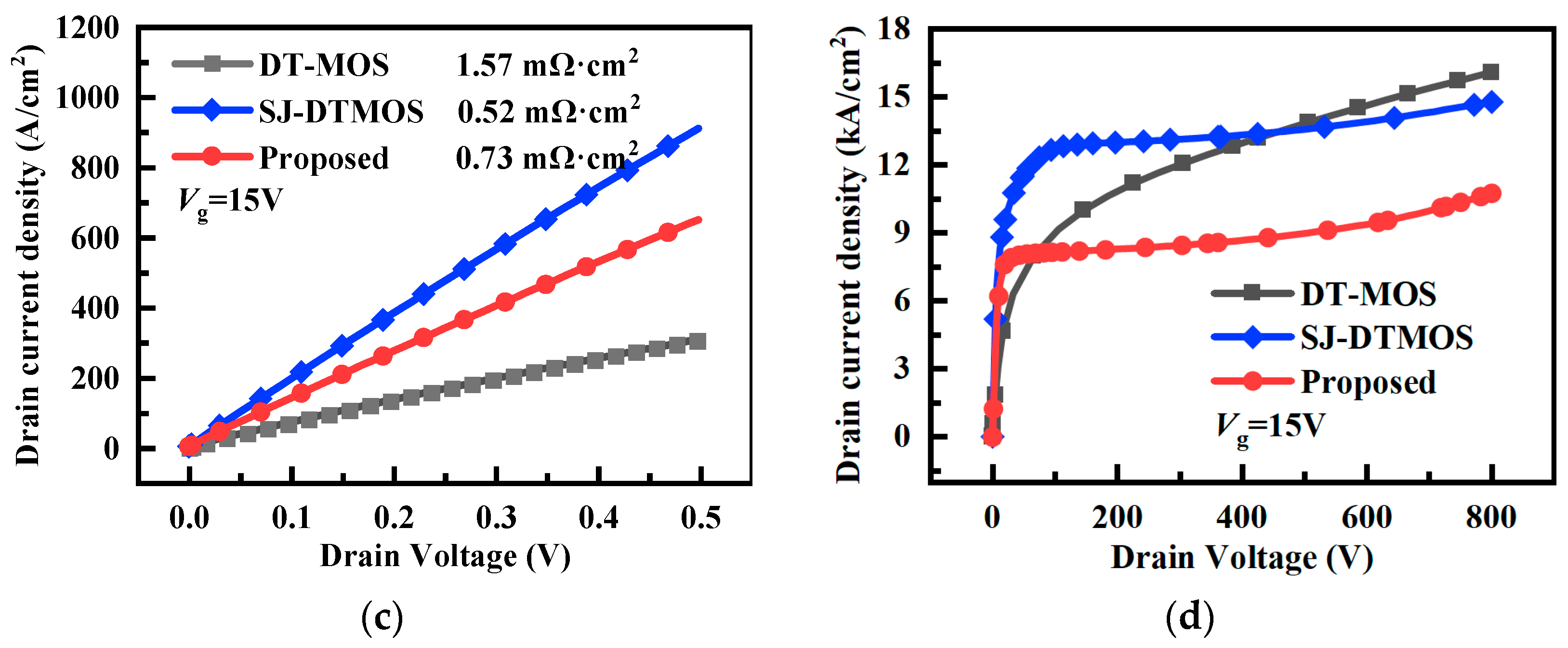
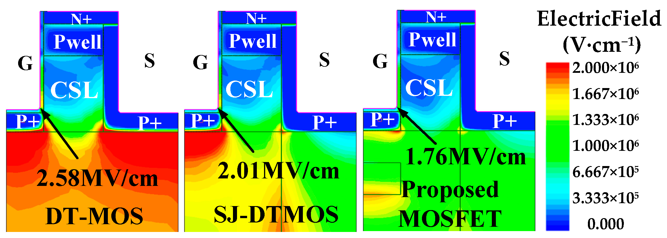
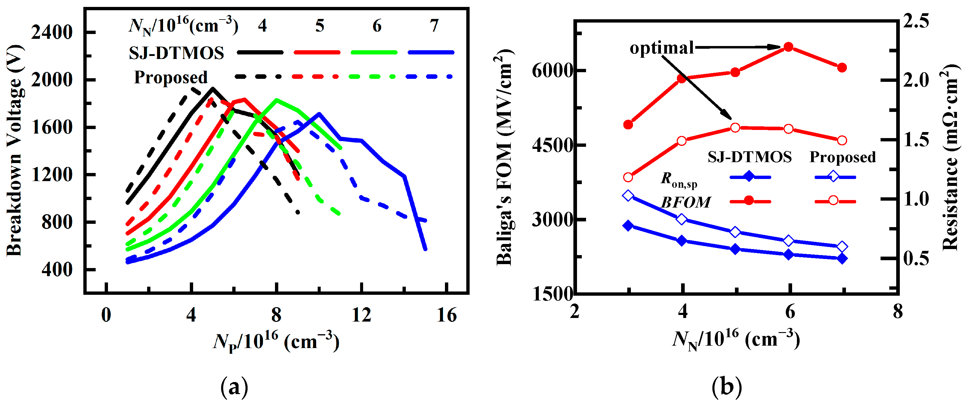
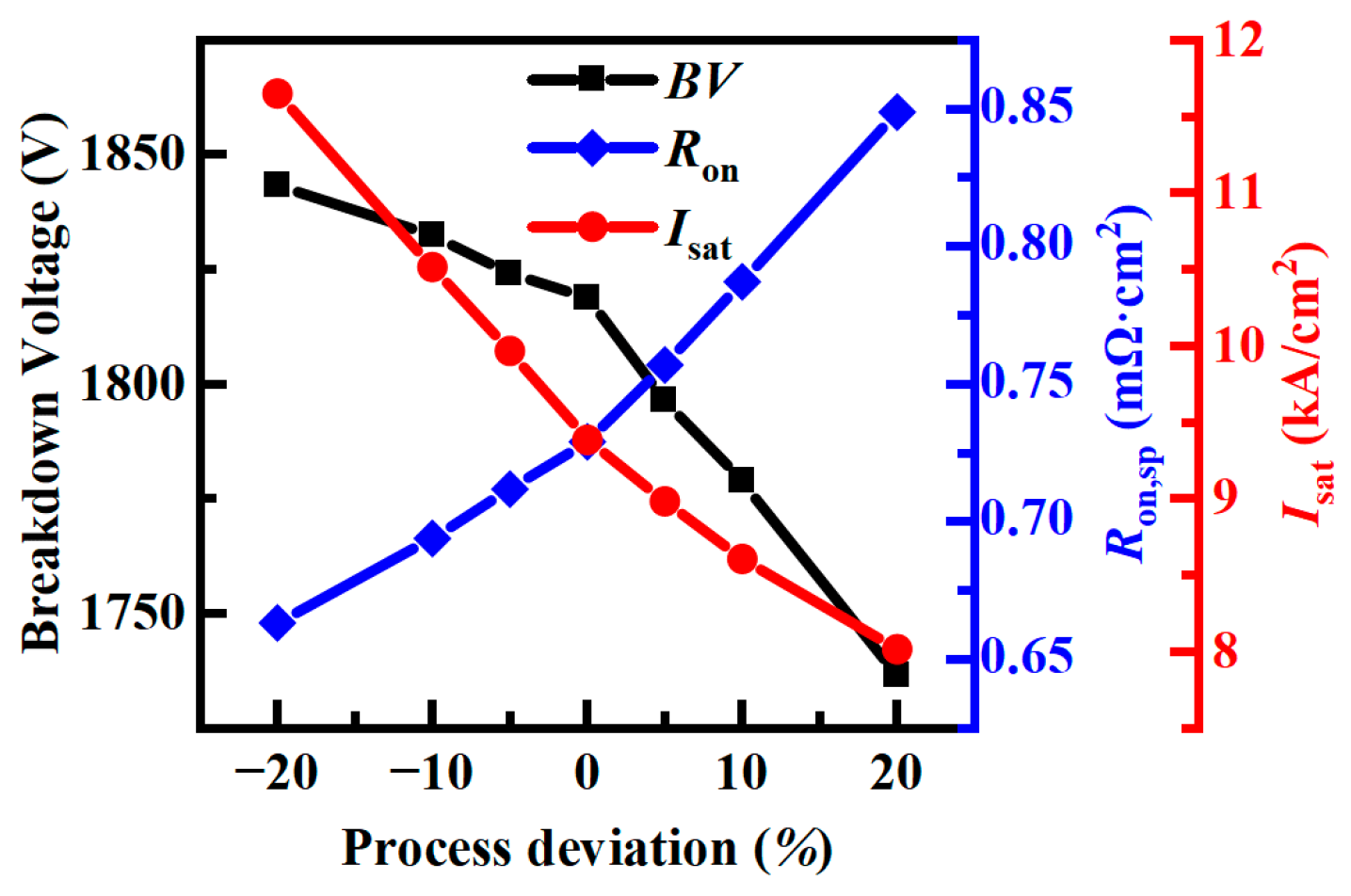
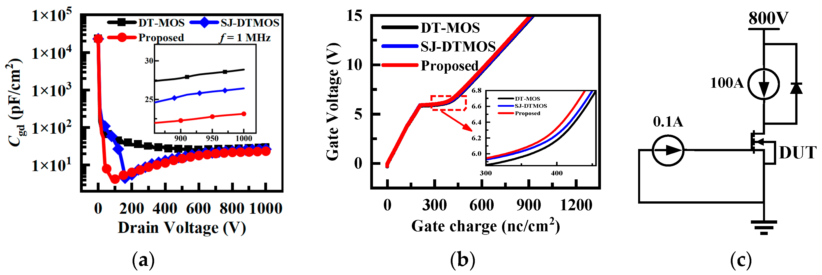
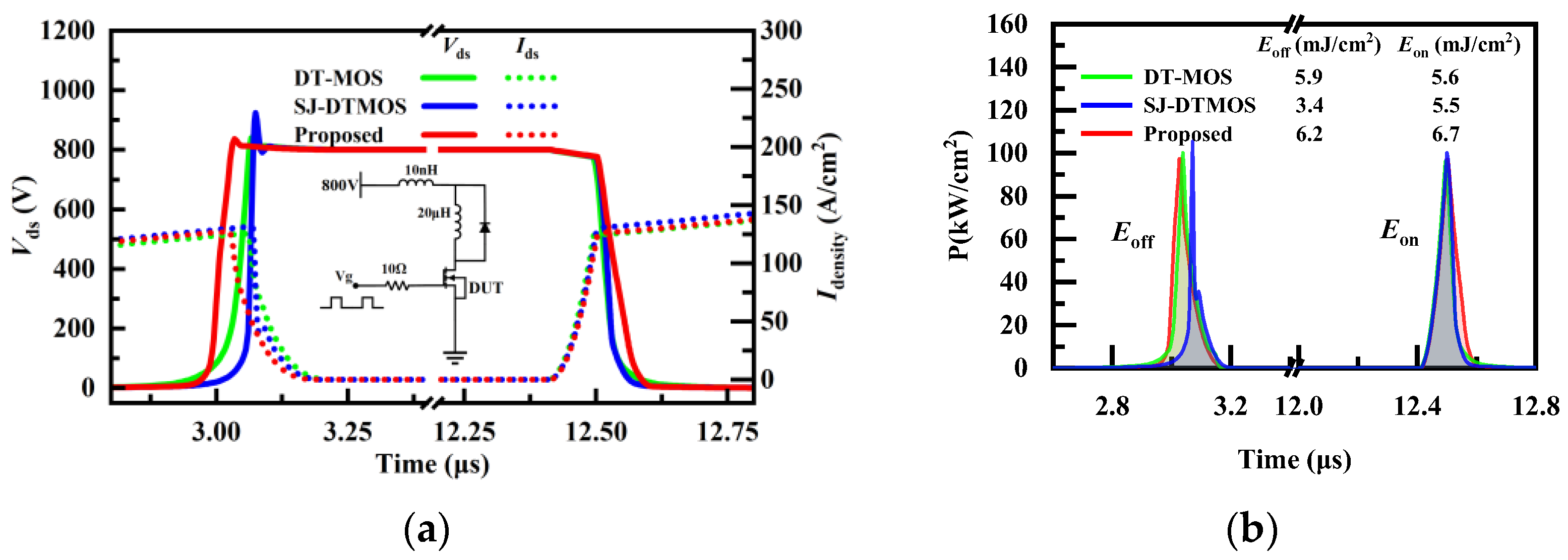
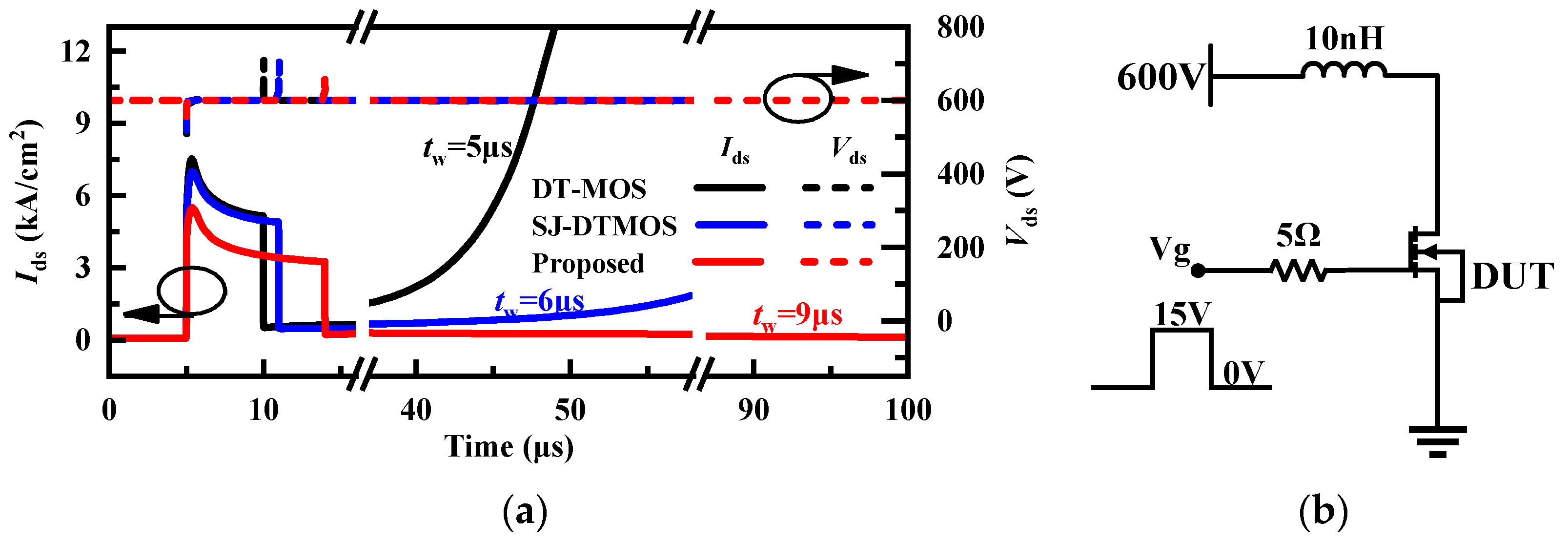
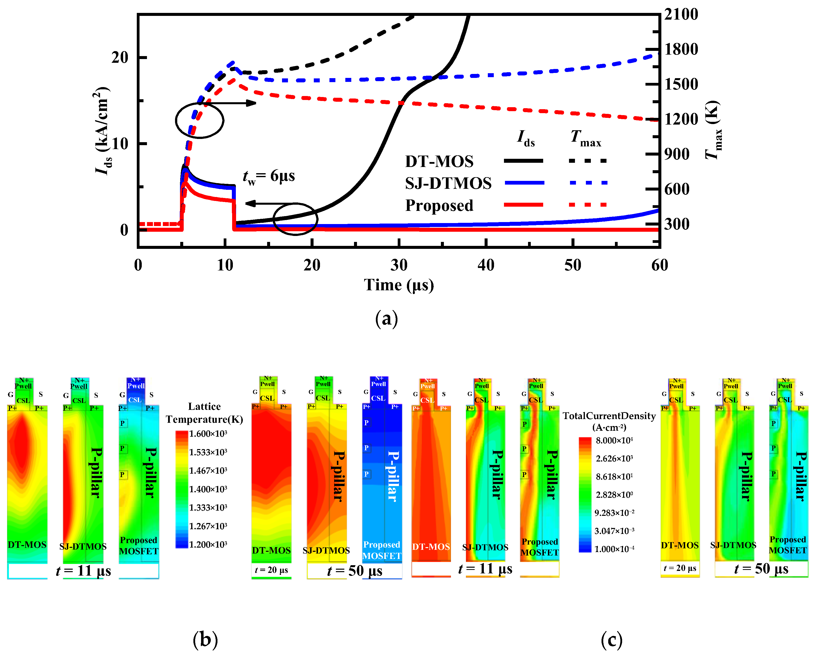
3. Simulation Results and Discussion
4. Conclusions
Author Contributions
Funding
Data Availability Statement
Conflicts of Interest
References
- Hamada, K.; Nagao, M.; Ajioka, M.; Kawai, F. SiC—Emerging power device technology for next-generation electrically powered environmentally friendly vehicles. IEEE Trans. Electron Devices 2015, 62, 278–285. [Google Scholar] [CrossRef]
- Millan, J.; Godignon, P.; Perpina, X.; Perez-Tomas, A.; Rebollo, J. A survey of wide bandgap power semiconductor devices. IEEE Trans. Power Electron. 2014, 29, 2155–2163. [Google Scholar] [CrossRef]
- Palmour, J.W. Silicon Carbide Power Device Development for Industrial Markets. In Proceedings of the IEEE International Electron Devices Meeting (IEDM) 2014, San Francisco, CA, USA, 15–17 December 2014; pp. 1.1.1–1.1.8, ISBN 978-1-4799-8001-7. [Google Scholar]
- Zhou, X.; Pang, H.; Jia, Y.; Hu, D.; Wu, Y.; Tang, Y.; Xia, T.; Gong, H.; Zhao, Y. SiC Double-Trench MOSFETs with Embedded MOS-Channel Diode. IEEE Trans. Electron Devices 2020, 67, 582–587. [Google Scholar] [CrossRef]
- Luo, H.-C.; Wang, L.-M.; Wang, S.-G.; Tan, C.-J.; Zheng, K.; Zhang, G.-Q.; Tao, L.-Q.; Chen, X.-P. Investigations of SiC VDMOSFET with Floating Island Structure Based on TCAD. IEEE Trans. Electron Devices 2019, 66, 2295–2300. [Google Scholar] [CrossRef]
- Rabkowski, J.; Peftitsis, D.; Nee, H.-P. Silicon Carbide Power Transistors: A New Era in Power Electronics Is Initiated. IEEE Ind. Electron. Mag. 2012, 6, 17–26. [Google Scholar] [CrossRef]
- Williams, R.K.; Darwish, M.N.; Blanchard, R.A.; Siemieniec, R.; Rutter, P.; Kawaguchi, Y. The Trench Power MOSFET: Part I—History, Technology, and Prospects. IEEE Trans. Electron Devices 2017, 64, 674–691. [Google Scholar] [CrossRef]
- Kanale, A.; Baliga, B.J. Eliminating Repetitive Short-Circuit Degradation and Failure of 1.2-kV SiC Power MOSFETs. IEEE J. Emerg. Sel. Top. Power Electron. 2021, 9, 6773–6779. [Google Scholar] [CrossRef]
- Sun, J.; Xu, H.; Wu, X.; Sheng, K. Comparison and analysis of short circuit capability of 1200V single-chip SiC MOSFET and Si IGBT. In Proceedings of the 2016 13th China International Forum on Solid State Lighting: International Forum on Wide Bandgap Semiconductors China (SSLChina: IFWS), Beijing, China, 15–17 November 2016; pp. 42–45. [Google Scholar] [CrossRef]
- Zhou, H.; Ye, C.; Zhan, X.; Wang, Z. Designing a SiC MOSFETs Gate Driver with High dv/dt Immunity and Rapid Short Circuit Protection for xEV Drivetrain Inverter. In Proceedings of the 22nd International Conference on Electrical Machines and Systems, ICEMS 2019, Harbin, China, 11–14 August 2019. [Google Scholar] [CrossRef]
- Zuo, X.; Lu, J.; Tian, X.; Bai, Y.; Cheng, G.; Chen, H.; Tang, Y.; Yang, C.; Liu, X. Improvement on short-circuit ability of SiC super-junction MOSFET with partially widened pillar structure. Chin. Phys. B 2022, 31, 098502. [Google Scholar] [CrossRef]
- Bharti, D.; Islam, A. Optimization of SiC UMOSFET Structure for Improvement of Breakdown Voltage and ON-Resistance. IEEE Trans. Electron Devices 2017, 65, 615–621. [Google Scholar] [CrossRef]
- Nakamura, T.; Nakano, Y.; Aketa, M.; Nakamura, R.; Mitani, S.; Sakairi, H.; Yokotsujiet, Y. High Performance SiC Trench Devices with Ultra-low Ron. In Proceedings of the IEEE International Electron Devices Meeting (IEDM) 2011, Washington, DC, USA, 5–7 December 2011; pp. 26.5.1–26.5.3, ISBN 978-1-4577-0505-2. [Google Scholar]
- Yang, T.; Wang, Y.; Yue, R. SiC Trench MOSFET With Reduced Switching Loss and Increased Short-Circuit Capability. IEEE Trans. Electron Devices 2020, 67, 3685–3690. [Google Scholar] [CrossRef]
- Okawa, M.; Aiba, R.; Kanamori, T.; Kobayashi, Y.; Harada, S.; Yano, H.; Iwamuro, N. First Demonstration of Short-Circuit Capability for a 1.2 kV SiC SWITCH-MOS. IEEE J. Electron Devices Soc. 2019, 7, 613–620. [Google Scholar] [CrossRef]
- Li, X.; Deng, X.; Li, X.; Xu, X.; Wen, Y.; Wu, H.; Chen, W.; Zhang, B. A Novel SiC MOSFET With Embedded Auto-Adjust JFET With Improved Short Circuit Performance. IEEE Electron Device Lett. 2021, 42, 1751–1754. [Google Scholar] [CrossRef]
- Kim, D.; Sung, W. Improved Short-Circuit Ruggedness for 1.2kV 4H-SiC MOSFET Using a Deep P-Well Implemented by Channeling Implantation. IEEE Electron Device Lett. 2021, 42, 1822–1825. [Google Scholar] [CrossRef]
- Sentaurus Device User Guide, Version N-2017.09; Synopsys: Mountain View, CA, USA, 2017.
- Cao, W.; Yin, S.; Hu, X.; Li, M.; Ge, X.; Liu, D. A novel SiC superjunction MOSFET with three-level buffer and unipolar channel diode. Micro Nanostructures 2022, 172, 207420. [Google Scholar] [CrossRef]
- Jiang, H.; Wei, J.; Dai, X.; Ke, M.; Deviny, I.; Mawby, P. SiC Trench MOSFET With Shielded Fin-Shaped Gate to Reduce Oxide Field and Switching Loss. IEEE Electron Device Lett. 2016, 37, 1324–1327. [Google Scholar] [CrossRef]
- He, Q.; Luo, X.; Liao, T.; Wei, J.; Deng, G.; Sun, T.; Fang, J.; Yang, F. 4H-SiC superjunction trench MOSFET with reduced saturation current. Superlattices Microstruct. 2018, 125, 58–65. [Google Scholar] [CrossRef]
- Castro, I.; Roig, J.; Gelagaev, R.; Vlachakis, B.; Bauwens, F.; Lamar, D.G.; Driesen, J. Analytical Switching Loss Model for Superjunction MOSFET With Capacitive Nonlinearities and Displacement Currents for DC–DC Power Converters. IEEE Trans. Power Electron. 2016, 31, 2485–2495. [Google Scholar] [CrossRef]
- Kang, H.; Udrea, F. Dynamic CGD and dV/dt in Superjunction MOSFETs. IEEE Trans. Electron Devices 2020, 67, 1523–1529. [Google Scholar] [CrossRef]
- Sun, J.; Xu, H.; Wu, X.; Yang, S.; Guo, Q.; Sheng, K. Short circuit capability and high temperature channel mobility of SiC MOSFETs. In Proceedings of the 2017 29th International Symposium on Power Semiconductor Devices and IC’s (ISPSD), Sapporo, Japan, 28 May—1 June 2017; pp. 399–402. [Google Scholar]
- Harada, S.; Kobayashi, Y.; Kyogoku, S.; Morimoto, T.; Tanaka, T.; Takei, M.; Okumura, H. First Demonstration of Dynamic Characteristics for SiC Superjunction MOSFET Realized using Multi-epitaxial Growth Method. In Proceedings of the 2018 IEEE International Electron Devices Meeting (IEDM), San Francisco, CA, USA, 1–5 December 2018; pp. 8.2.1–8.2.4. [Google Scholar] [CrossRef]
- Masuda, T.; Saito, Y.; Kumazawa, T.; Hatayama, T.; Harada, S. 0.63 mΩcm2/1170 V 4H-SiC Super Junction V-Groove Trench MOSFET. In Proceedings of the 2018 IEEE International Electron Devices Meeting (IEDM), San Francisco, CA, USA, 1–5 December 2018; pp. 8.1.1–8.1.4. [Google Scholar]


| Device Parameters | DT-MOS | SJ-DTMOS | Proposed |
|---|---|---|---|
| N-pillar or N-drift doping (cm−3) | 8 × 10¹⁵ | 6 × 10¹⁶ | 5 × 10¹⁶ |
| P-pillar doping (cm−3) | — | 8 × 10¹⁶ | 5 × 10¹⁶ |
| Number of floating p-region (n) | — | — | 3 |
| Floating p-region doping (cm−3) | — | — | 1.5 × 10¹⁷ |
| s (μm) | — | — | 0.5 |
| h (μm) | — | — | 0.5 |
| w (μm) | — | — | 0.5 |
| d (μm) | — | — | 1.0 |
| Symbol | DT-MOS | SJ-DTMOS | Proposed MOSFET |
|---|---|---|---|
| BV (V) | 1799 | 1829 | 1819 |
| Ron,sp 1 (mΩ·cm2) | 1.57 | 0.52 | 0.73 |
| Eox 2 (MV/cm) | 2.04 | 2.01 | 1.76 |
| Qgd (nC/cm2) | 179 | 153 | 144 |
| Cgd 3 (pF/cm2) | 28.8 | 26.4 | 23.1 |
| Eon 4 (mJ/cm2) | 5.6 | 5.5 | 6.7 |
| Eoff 5 (mJ/cm2) | 5.9 | 3.4 | 6.2 |
| Etotal 6 (mJ/cm2) | 11.5 | 8.9 | 12.9 |
| Rd1 7 (mΩ·cm2) | 1.78 | 0.89 | 1.27 |
| Rd10 8 (mΩ·cm2) | 2.26 | 0.93 | 1.41 |
| tsc (μs) | 4 | 5 | 9 |
Disclaimer/Publisher’s Note: The statements, opinions and data contained in all publications are solely those of the individual author(s) and contributor(s) and not of MDPI and/or the editor(s). MDPI and/or the editor(s) disclaim responsibility for any injury to people or property resulting from any ideas, methods, instructions or products referred to in the content. |
© 2023 by the authors. Licensee MDPI, Basel, Switzerland. This article is an open access article distributed under the terms and conditions of the Creative Commons Attribution (CC BY) license (https://creativecommons.org/licenses/by/4.0/).
Share and Cite
Yin, S.; Cao, W.; Hu, X.; Ge, X.; Liu, D. A Novel Super-Junction DT-MOS with Floating p Regions to Improve Short-Circuit Ruggedness. Micromachines 2023, 14, 1962. https://doi.org/10.3390/mi14101962
Yin S, Cao W, Hu X, Ge X, Liu D. A Novel Super-Junction DT-MOS with Floating p Regions to Improve Short-Circuit Ruggedness. Micromachines. 2023; 14(10):1962. https://doi.org/10.3390/mi14101962
Chicago/Turabian StyleYin, Sujie, Wei Cao, Xiarong Hu, Xinglai Ge, and Dong Liu. 2023. "A Novel Super-Junction DT-MOS with Floating p Regions to Improve Short-Circuit Ruggedness" Micromachines 14, no. 10: 1962. https://doi.org/10.3390/mi14101962
APA StyleYin, S., Cao, W., Hu, X., Ge, X., & Liu, D. (2023). A Novel Super-Junction DT-MOS with Floating p Regions to Improve Short-Circuit Ruggedness. Micromachines, 14(10), 1962. https://doi.org/10.3390/mi14101962