
An Investigation on the Most Likely Failure Locations in the BEoL Stack of a 20 nm Chip Due to Chip Package Interaction with the Use of Novel Semi-Elliptical Cracks

Abstract
:1. Introduction
2. Modeling of BEoL Stack
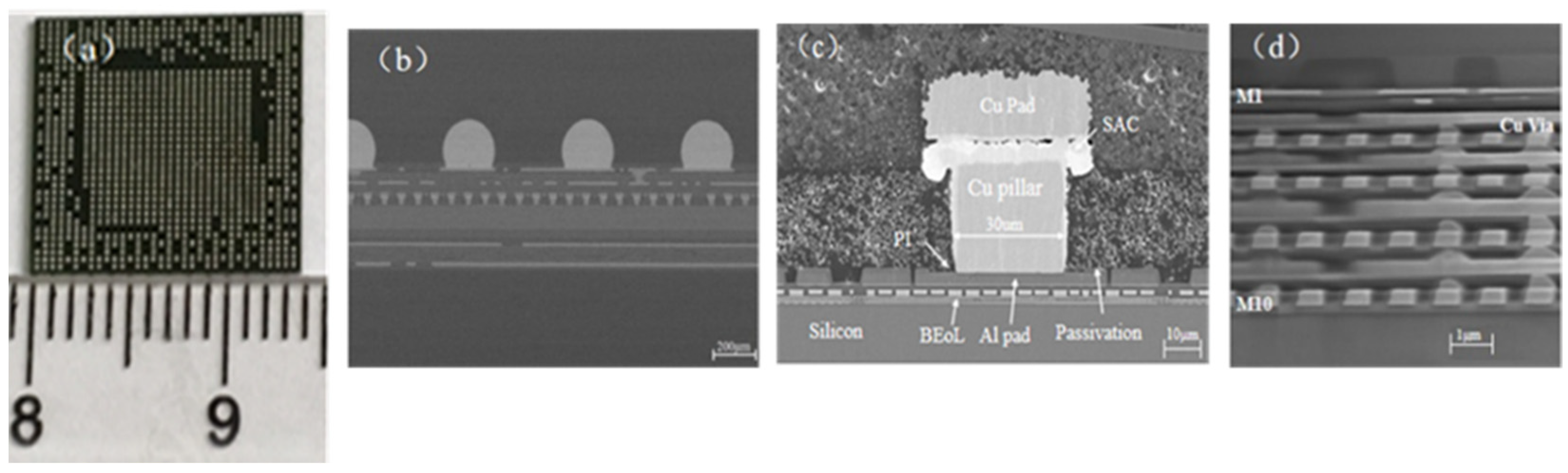
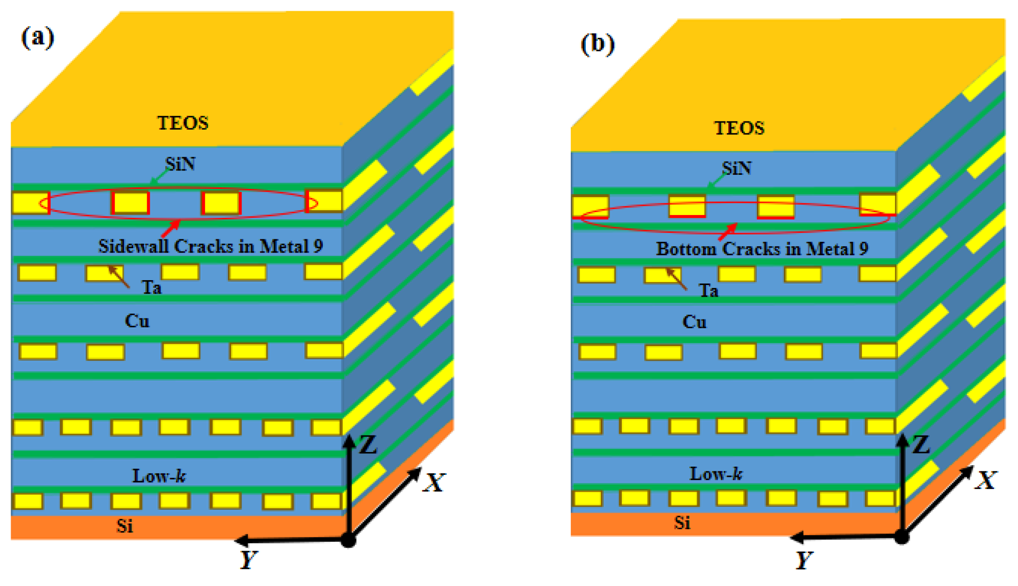
2.1. Details of the BEoL Stack of the 20 nm Chip
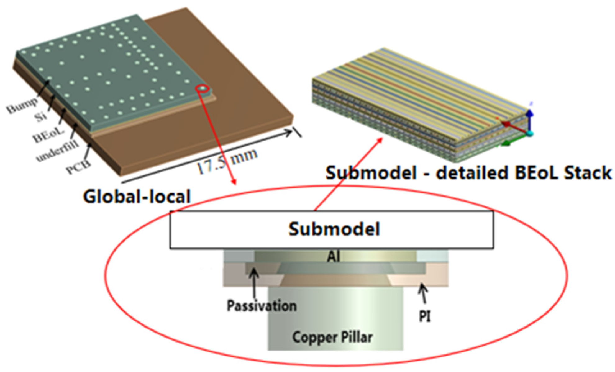
2.2. “Global-Local”Finite-Element Models
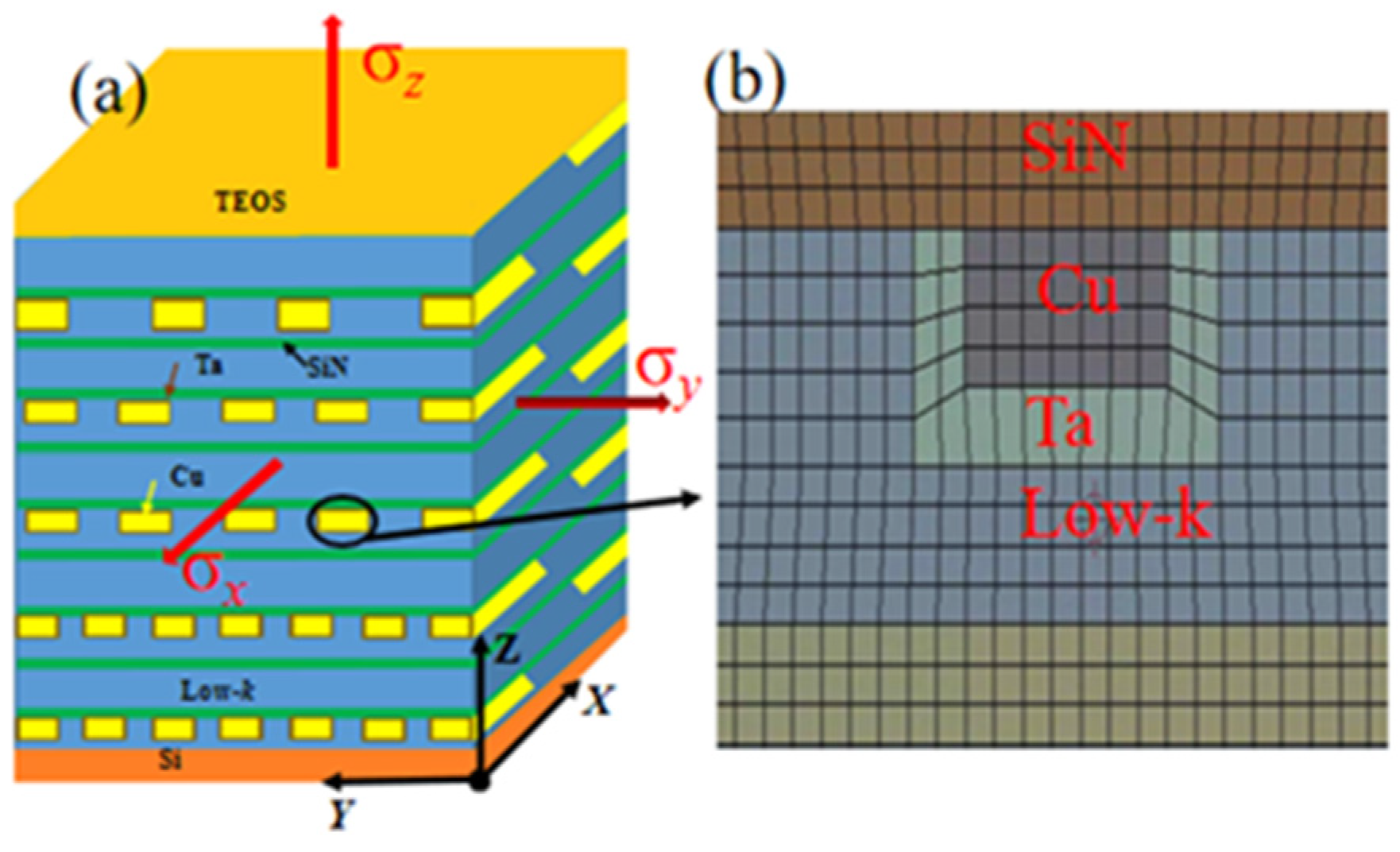
2.2.1. Effective Mechanical Properties of the BEoL Stack
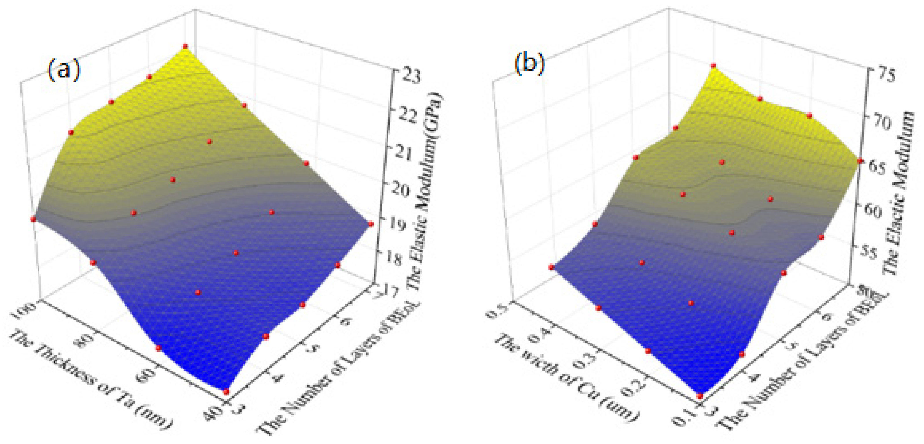
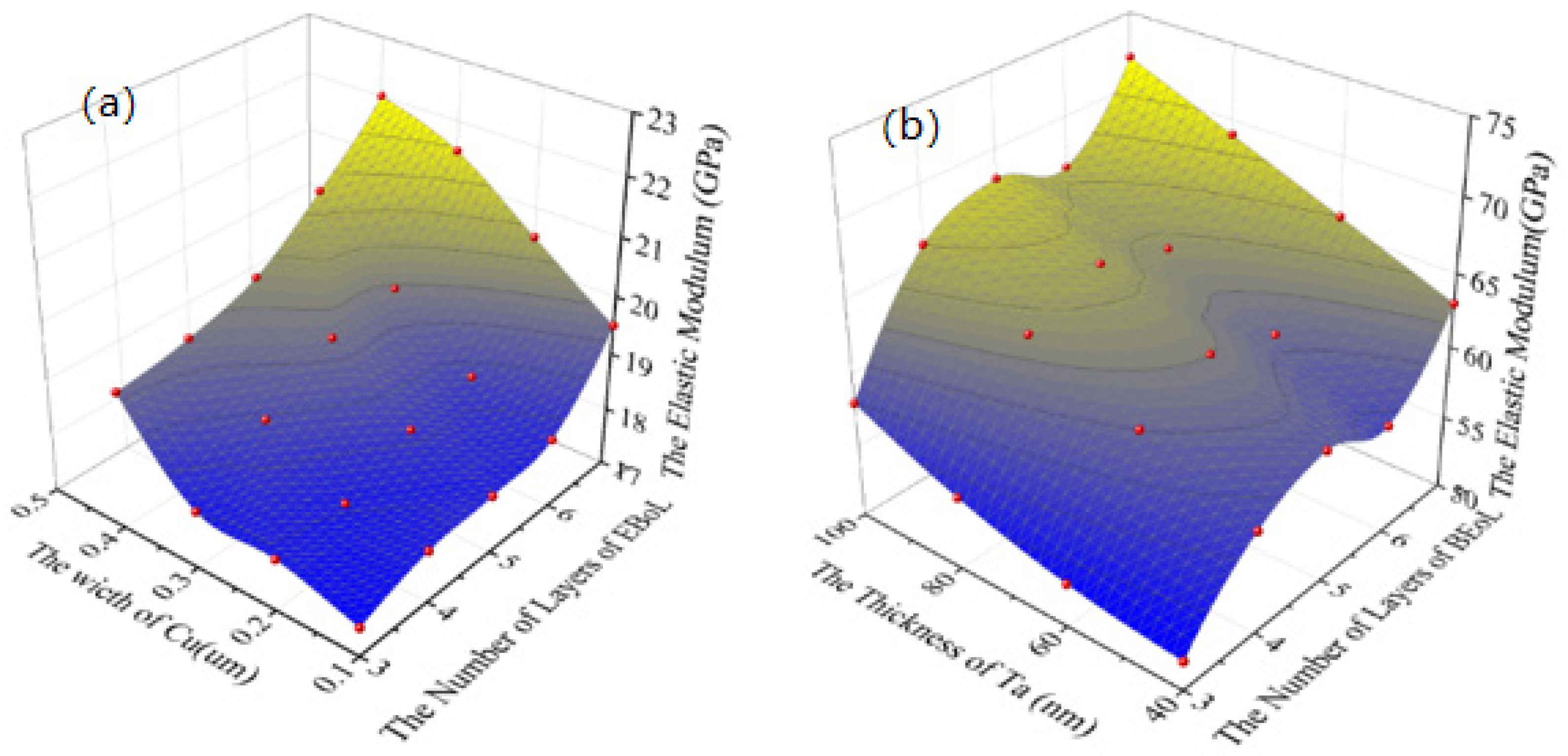
2.2.2. Effect of the Width of the Cu Interconnects and the Number of Layers of BEoL Stack on the Equivalent Elastic Modulus
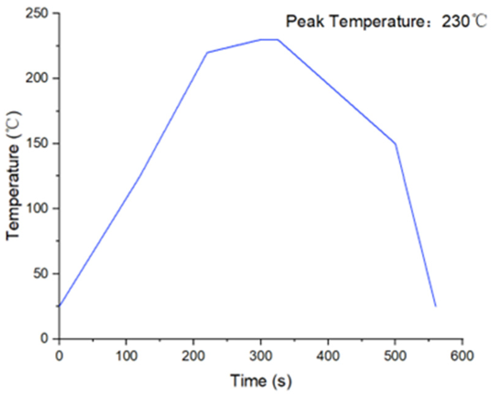
2.2.3. Thermal Stress in BEoL Stack during Solder Reflow
3. Study on the Most Likely Failure Location of BEoL Stack
3.1. Competitive Failure of Cracks along Different Interfaces
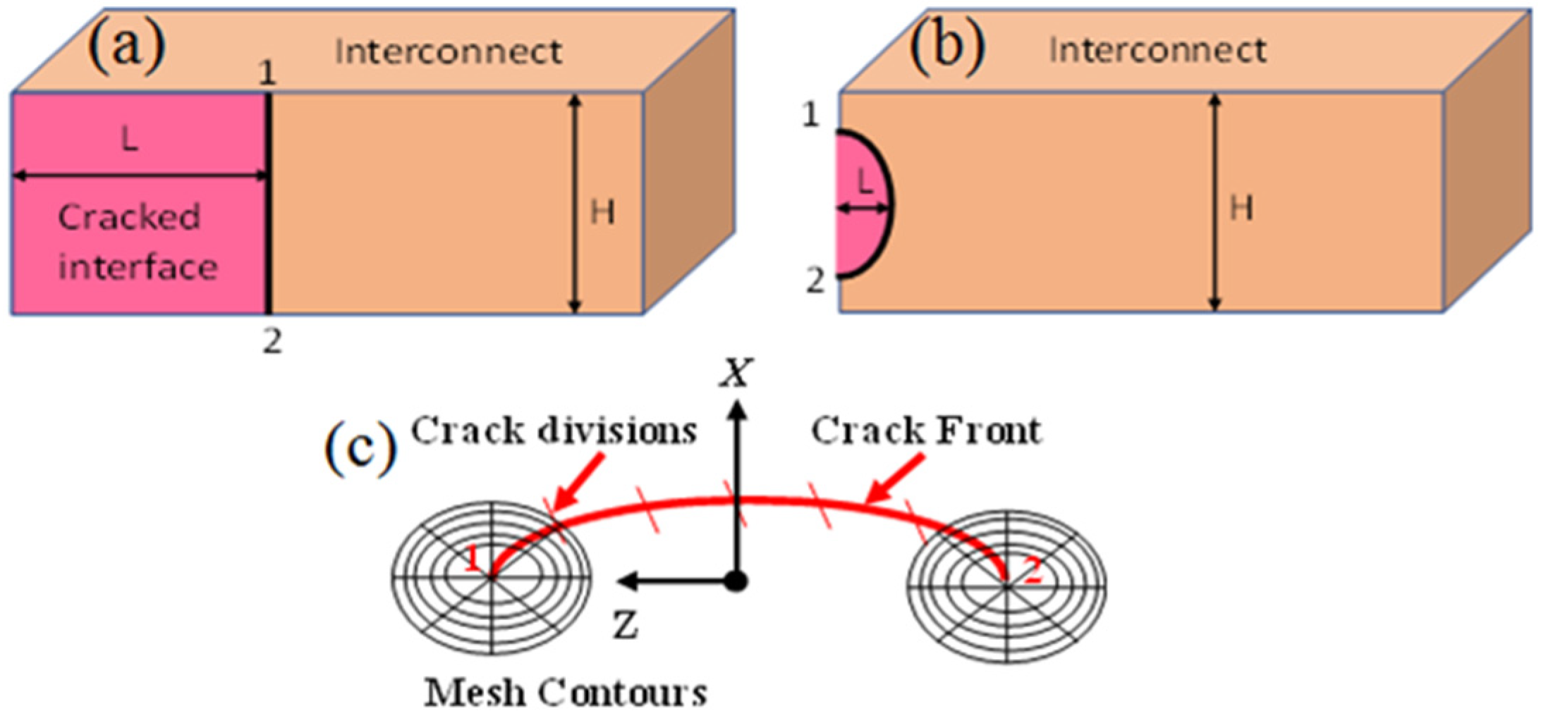
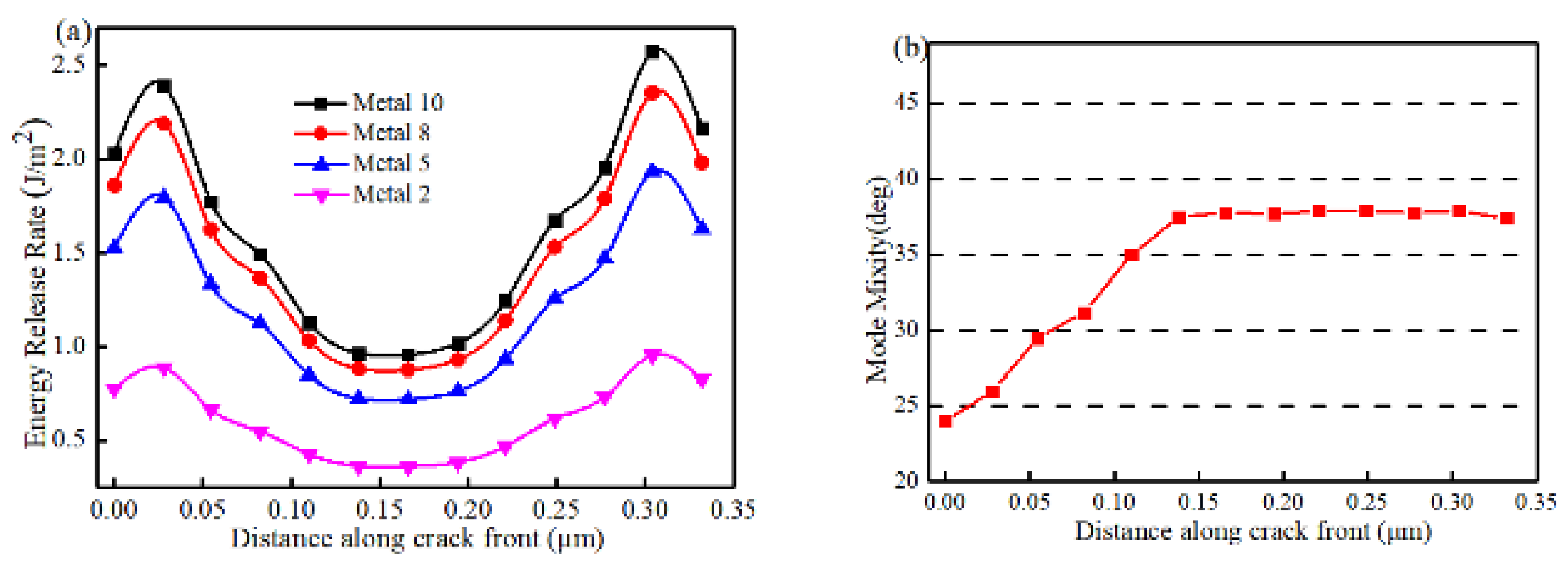
3.2. Variation of ERR along the Semi-Elliptical Crack Front
3.3. Variation of ERR with Metal Layer Number
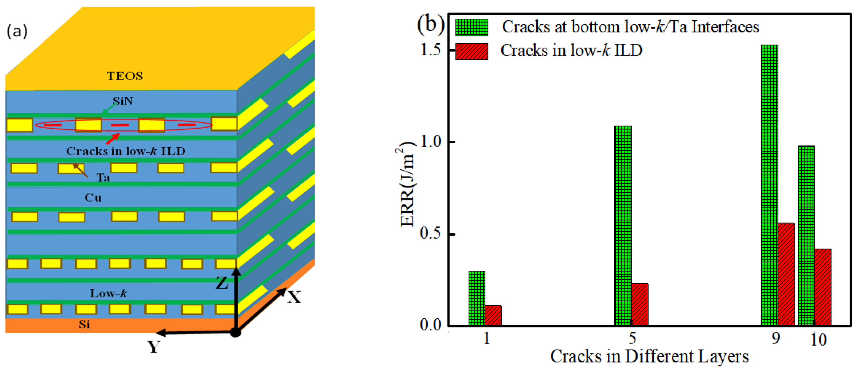
3.4. Competitive Failure between Interfacial Cracks and Cracks in the Low-k ILD
4. Experimental Study on Failure of BEoL Stack
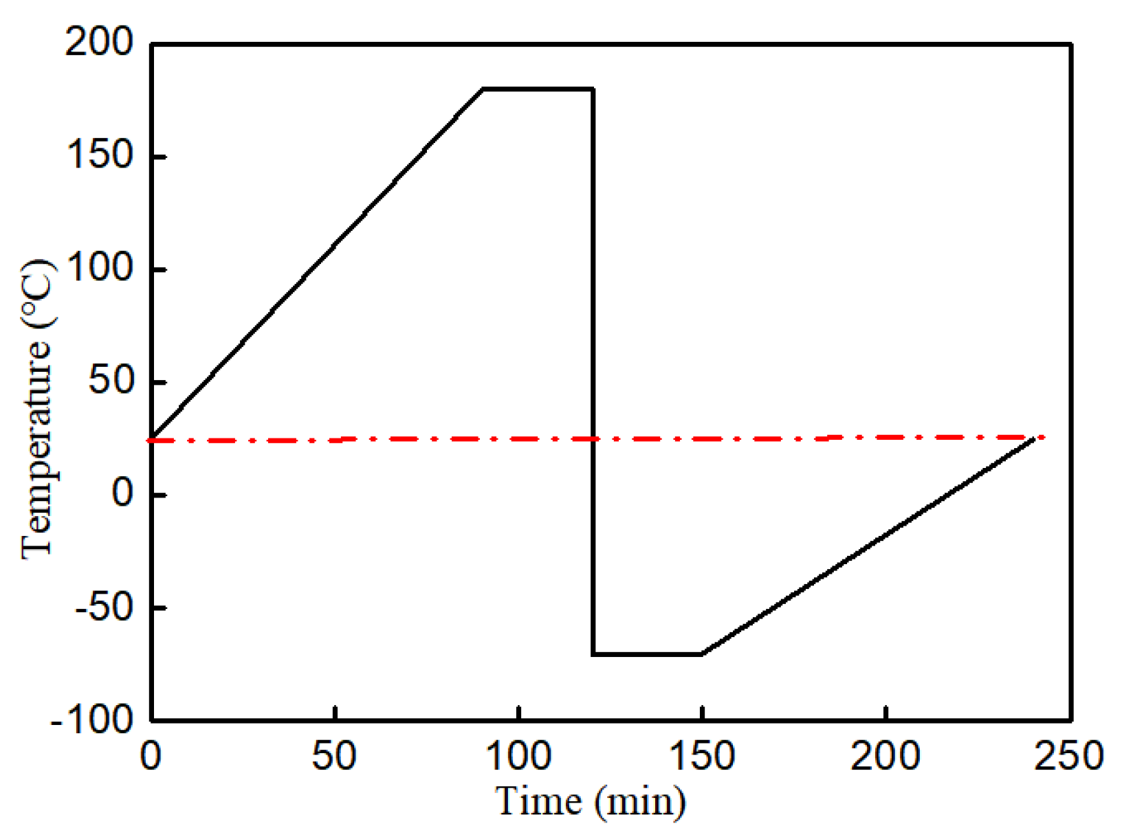
4.1. Experimental Procedure
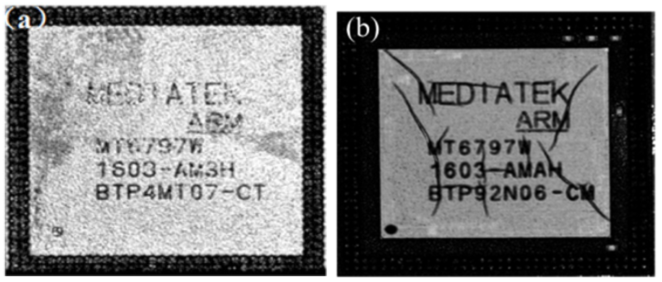
4.2. Experimental Results
5. Conclusions
- (1)
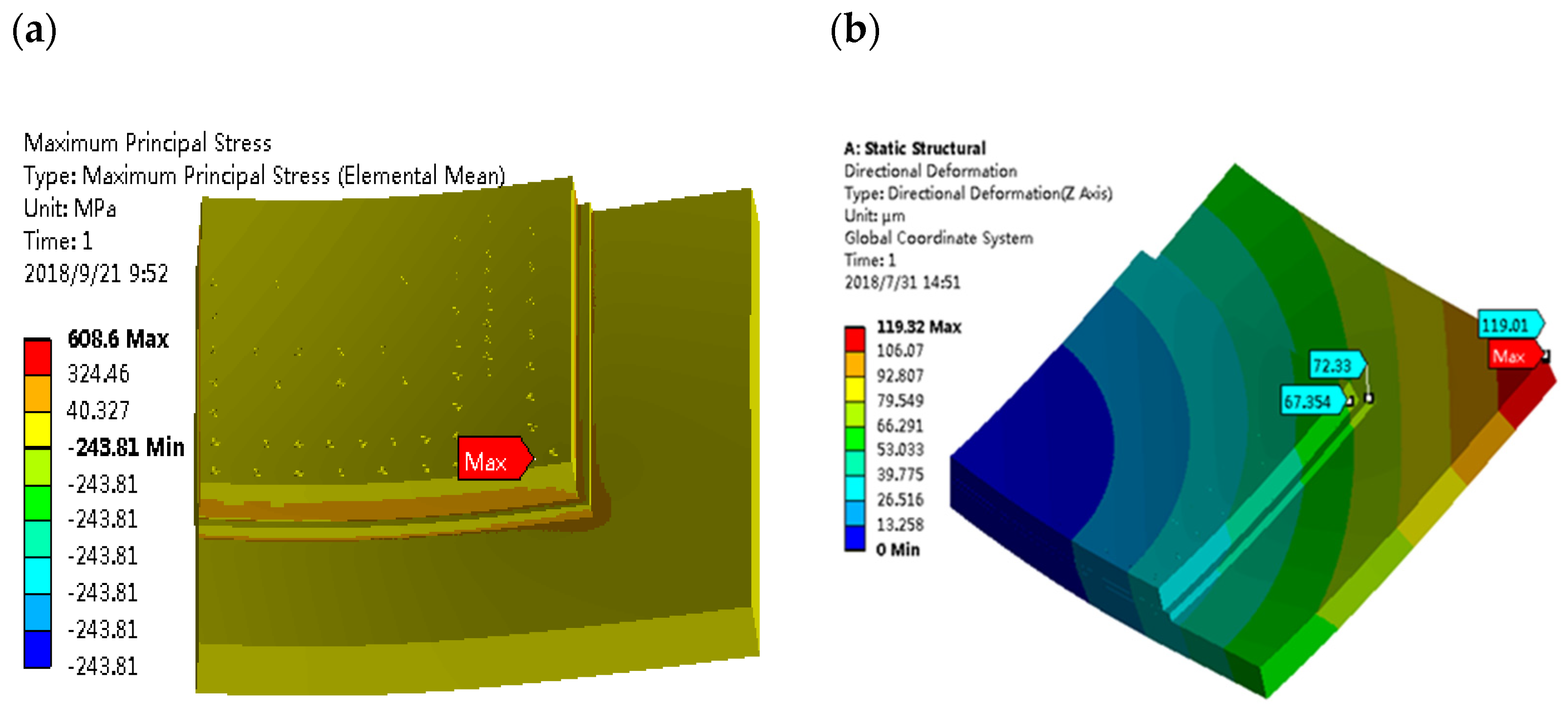
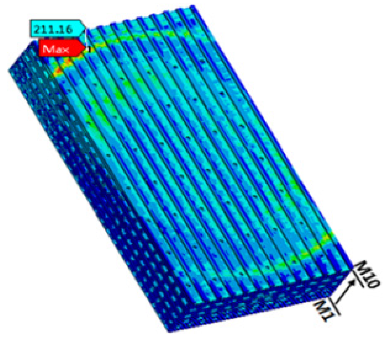
- The microbumps furthest from the center of the chip have the greatest stress, and accordingly the largest PCB warpage.
- (2)
- The crack ERR of the low-k/Ta interfaces are higher than that for cracks within the low-k material.
- (3)
- Interfacial cracks in the M9 layer in the BEoL structure have the largest ERR among all layers and are hence more likely to propagate.
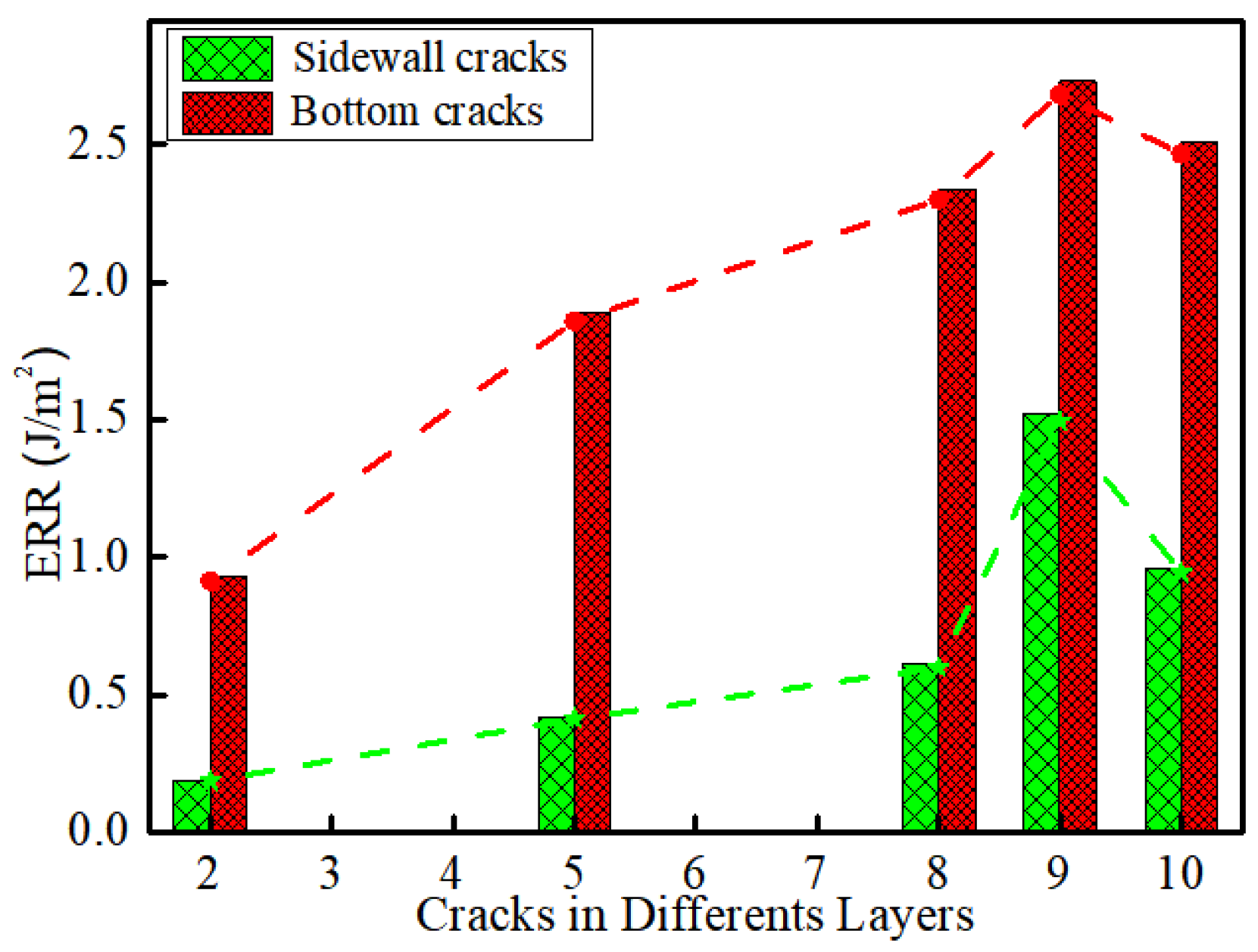
- (4)
- The interfacial crack at the bottom of the interconnect is more likely to propagate than that at the sidewalls of the interconnect.
- (5)
- The thermal shock experiments demonstrated that the dominant failure mode is the delamination in the second outer layer of the metal layer in the manner of Ta/low-k interfacial cracking at the bottom.
Author Contributions
Funding
Data Availability Statement
Conflicts of Interest
References
- Zhang, J.; Zhang, G.; Gao, Y.; Sun, R.; Wong, C.P. Ultra-low-κHFPDB-based periodic mesoporous organosilica film with high mechanical strength for interlayer dielectric. J. Mater. Sci. 2016, 51, 7966–7976. [Google Scholar] [CrossRef]
- Xiao, C.; He, H.; Li, J.; Cao, S.; Zhu, W. An effective and efficient numerical method for thermal management in 3D stacked integrated circuits. Appl. Therm. Eng. 2017, 121, 200–209. [Google Scholar] [CrossRef]
- Li, H.; Tie, J.; Li, J.; Ye, M.; Zhang, H.; Zhang, X.; Pan, Y.; Wang, Y.; Quhe, R.; Pan, F. High-performance sub-10-nm monolayer black phosphorene tunneling transistors. Nano Res. 2017, 11, 2658–2668. [Google Scholar] [CrossRef]
- Fu, S.; Qian, K.; Ding, S.; Zhang, W.; Fan, Z. Characterization of ultra-low k porous organosilica thin films. In Proceedings of the IEEE International Conference on Solid-State and Integrated Circuit Technology, Shanghai, China, 1–4 November 2010; pp. 1033–1035. [Google Scholar]
- Li, G.; Zheng, G.; Ding, Z.; Shi, L.; Li, J.; Chen, Z.; Wang, L.; Tay, A.A.O.; Zhu, W. High-performance ultra-low-k fluorine-doped nanoporousorganosilica films for inter-layer dielectric. J. Mater. Sci. 2018, 54, 2379–2391. [Google Scholar] [CrossRef]
- Chai, T.C.; Zhang, X.; Li, H.Y.; Sekhar, V.N.; Hnin, W.Y.; Thew, M.L.; Navas, O.K.; Lau, J.; Mruthy, R.; Balakumar, S.; et al. Impact of packaging design on reliability of large die Cu/low-k interconnect. In Proceedings of the 2008 58th Electronic Components and Technology Conference, Lake Buena Vista, FL, USA, 27–30 May 2008; pp. 38–45. [Google Scholar]
- Bao, A.; Zhao, L.; Sun, Y.; Han, M.; Lee, K. Challenges and opportunities of chip package interaction with fine pitch Cu pillar for 28 nm. In Proceedings of the 2014 IEEE 64th Electronic Components and Technology Conference (ECTC), Lake Buena Vista, FL, USA, 27–30 May 2014. [Google Scholar]
- Jacob, P. Surface ESD (ESDFOS) in assembly fab machineries as a functional and reliability risk—Failure analysis, tool diagnosis and on-site-remedies. Microelectron Reliab. 2008, 48, 1608–1612. [Google Scholar] [CrossRef]
- Ryan, V.; Breuer, D.; Geisler, H.; Kioussis, D.; Karimanal, K. CPI challenges to BEOL at 28 nm node and beyond. In Proceedings of the IEEE International Reliability Physics Symposium, Anaheim, CA, USA, 15–19 April 2012. [Google Scholar]
- Lei, M.; Goldberg, C.; Kuo, S.M. A simulation method for predicting packaging mechanical reliability with low/spl kappa/dielectrics. In Proceedings of the IEEE 2002 International Interconnect Technology Conference (Cat. No.02EX519), Burlingame, CA, USA, 5 June 2002. [Google Scholar]
- Mercado, L.; Goldberg, C.; Kuo, S.-M.; Lee, T.-Y.; Pozder, S.; Yu, T.; Lee, T. Analysis of flip-chip packaging challenges on copper/low-k interconnects. IEEE Trans. Device Mater. Reliab. 2003, 3, 111–118. [Google Scholar] [CrossRef]
- Zhang, X.; Wang, Y.; Im, J.H.; Ho, P.S. Chip–Package Interaction and Reliability Improvement by Structure Optimization for Ultralow-$k$ Interconnects in Flip-Chip Packages. IEEE Trans. Device Mater. Reliab. 2012, 12, 462–469. [Google Scholar] [CrossRef]
- Liu, X.H.; Shaw, T.M.; Lane, M.W.; Liniger, E.G.; Questad, D.L. Chip-Package-Interaction Modeling of Ultra Low-k/Copper Back End of Line. In Proceedings of the IEEE International Interconnect Technology Conference, Burlingame, CA, USA, 4–6 June 2007. [Google Scholar]
- Wang, G.; Ho, P.S.; Groothuis, S. Chip-packaging interaction: A critical concern for C/low k packaging. Microelectron. Reliab. 2005, 45, 1079–1093. [Google Scholar] [CrossRef]
- Wang, G. Thermal Deformation of Electronic Packages and Packaging Effect on Reliability for Copper/Low-k Interconnect Structures; The University of Texas at Austin ProQuest Dissertations Publishing: Austin, TX, USA, 2008. [Google Scholar]
- Wang, G.; Groothuis, S.; Merrill, C.; Ho, P.S. Investigation of interfacial delamination for Cu/low k structures during flip-chip packaging. In Proceedings of the Conference on Thermal & Thermomechanical Phenomena in Electronic Systems, Las Vegas, NV, USA, 1–4 June 2004. [Google Scholar]
- Gao, S.; Smith, R.S.; Cho, J.K.; Choi, S.; Kannan, S.; Chua, E.; Geisler, H.; Kuechenmeister, F. Chip Packaging Interaction (CPI) with Cu Pillar Flip Chip for 20 nm Silicon Technology and Beyond. ECS J. Solid. State Sci. Technol. 2014, 4, N3134–N3139. [Google Scholar] [CrossRef]
- Uchibori, C.J.; Ho, P.S.; Nakamura, T. Chip Package Interaction and Mechanical Reliability Impact on Cu/ultra low-k Interconnects in Flip Chip Package. In Proceedings of the International Conference on Solid-state & Integrated-Circuit Technology, Beijing, China, 20–23 October2008. [Google Scholar]
- Tambat, A.; Lin, H.Y.; Subbarayan, G.; Jung, D.Y.; Sammakia, B. Simulations of Damage, Crack Initiation, and Propagation in Interlayer Dielectric Structures: Understanding Assembly-Induced Fracture in Dies. IEEE Trans. Device Mater. Reliab. 2012, 12, 241–254. [Google Scholar] [CrossRef]


| Component | Dimensions (h = Height, D = Diameter) |
|---|---|
| Si | 6.8 mm × 6.8 mm × 150 μm |
| PCB | 15 mm × 15 mm × 190 μm |
| SAC | D = 30 μm, h = 5 μm |
| Copper pillar | D = 30 μm, h = 20 μm |
| Cu Pad | D = 30 μm, h = 10 μm |
| BEoL layer | h = 8.2 μm |
| Al Pad | D = 20 μm, h = 3 μm |
| PI layer | D = 25 μm, h = 4 μm |
| Underfill | 7 mm × 7 mm × 59 μm |
| passivation | h = 4 μm |
| Material | Elastic Moudulus(GPa) | Poisson’s Ratio | Themal Expansion Coefficient (ppm) |
|---|---|---|---|
| Cu | 130 | 0.35 | 17.4 |
| Ta | 195 | 0.3 | 6.5 |
| Low-k | 10.6 | 0.3 | 15 |
| Underfill | 14.5 | 0.34 | α1/α2:25/110; Tg = 135 °C |
| SiN | 200 | 0.27 | 3 |
| Passivation | 211 | 0.27 | 3.2 |
| Si | 129 | 0.28 | 2.9 |
| Al | 74 | 0.33 | 21.5 |
| PI | 3.5 | 0.34 | 35 |
| SAC | 43 | 0.3 | 21.3 + 0.0175T (°C) |
| Material | Pitch (nm) | Width (nm) | Thickness (nm) | Barrier Thickness (nm) | Etched Layer Thickness (nm) |
|---|---|---|---|---|---|
| Metal 1 | 200 | 800 | 400 | 30 | 40 |
| Metal 2 | 200 | 800 | 400 | 30 | 40 |
| Metal 3 | 200 | 800 | 400 | 30 | 40 |
| Metal 4 | 300 | 850 | 500 | 40 | 45 |
| Metal 5 | 300 | 850 | 500 | 40 | 45 |
| Metal 6 | 300 | 850 | 500 | 40 | 45 |
| Metal 7 | 500 | 900 | 600 | 50 | 60 |
| Metal 8 | 500 | 900 | 600 | 50 | 60 |
| Metal 9 | 500 | 900 | 600 | 50 | 60 |
| Metal 10 | 700 | 1050 | 700 | 60 | 60 |
| Si | 750 |
Disclaimer/Publisher’s Note: The statements, opinions and data contained in all publications are solely those of the individual author(s) and contributor(s) and not of MDPI and/or the editor(s). MDPI and/or the editor(s) disclaim responsibility for any injury to people or property resulting from any ideas, methods, instructions or products referred to in the content. |
© 2023 by the authors. Licensee MDPI, Basel, Switzerland. This article is an open access article distributed under the terms and conditions of the Creative Commons Attribution (CC BY) license (https://creativecommons.org/licenses/by/4.0/).
Share and Cite
Li, G.; Shi, Y.; Tay, A.A.O.; Long, Z. An Investigation on the Most Likely Failure Locations in the BEoL Stack of a 20 nm Chip Due to Chip Package Interaction with the Use of Novel Semi-Elliptical Cracks. Micromachines 2023, 14, 1953. https://doi.org/10.3390/mi14101953
Li G, Shi Y, Tay AAO, Long Z. An Investigation on the Most Likely Failure Locations in the BEoL Stack of a 20 nm Chip Due to Chip Package Interaction with the Use of Novel Semi-Elliptical Cracks. Micromachines. 2023; 14(10):1953. https://doi.org/10.3390/mi14101953
Chicago/Turabian StyleLi, Ganglong, Yidian Shi, Andrew A. O. Tay, and Zhilin Long. 2023. "An Investigation on the Most Likely Failure Locations in the BEoL Stack of a 20 nm Chip Due to Chip Package Interaction with the Use of Novel Semi-Elliptical Cracks" Micromachines 14, no. 10: 1953. https://doi.org/10.3390/mi14101953
APA StyleLi, G., Shi, Y., Tay, A. A. O., & Long, Z. (2023). An Investigation on the Most Likely Failure Locations in the BEoL Stack of a 20 nm Chip Due to Chip Package Interaction with the Use of Novel Semi-Elliptical Cracks. Micromachines, 14(10), 1953. https://doi.org/10.3390/mi14101953