
A D-Band Direct-Conversion IQ Receiver with 28 dB CG and 7.3 dB NF in 130 nm SiGe Process
 , ,
, ,
Abstract
:1. Introduction
2. Receiver Architecture and Building Block
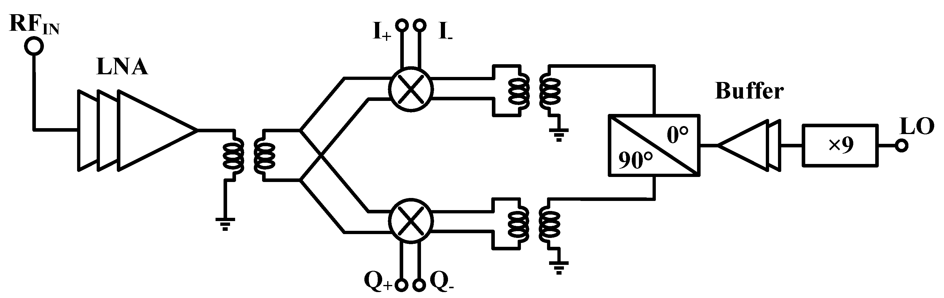
2.1. The Direct Conversion IQ Receiver
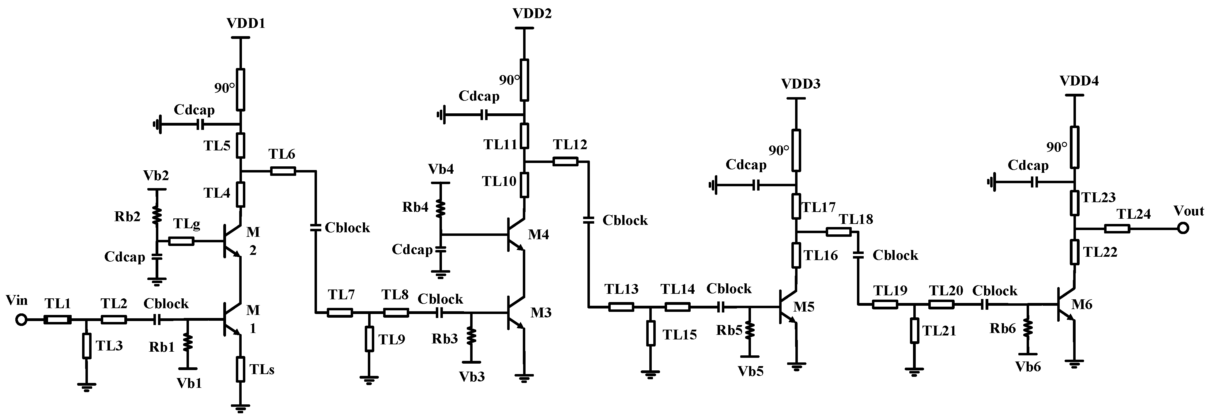
2.2. The D-Band LNA
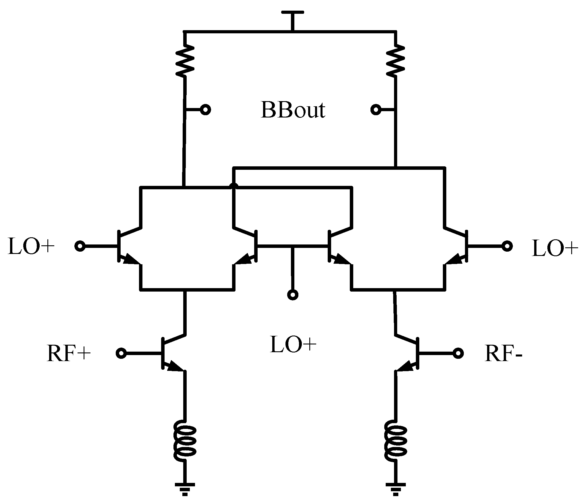
2.3. The Mixer
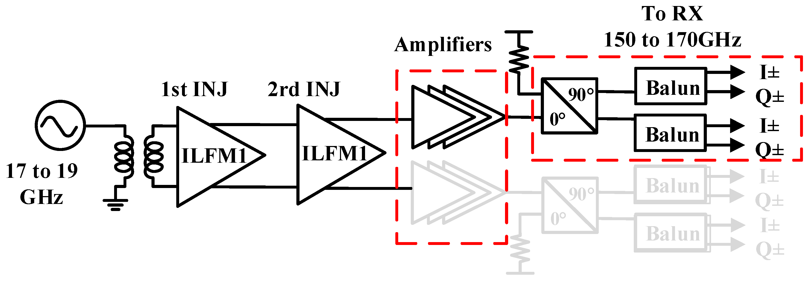
2.4. The LO Multiplier Chain
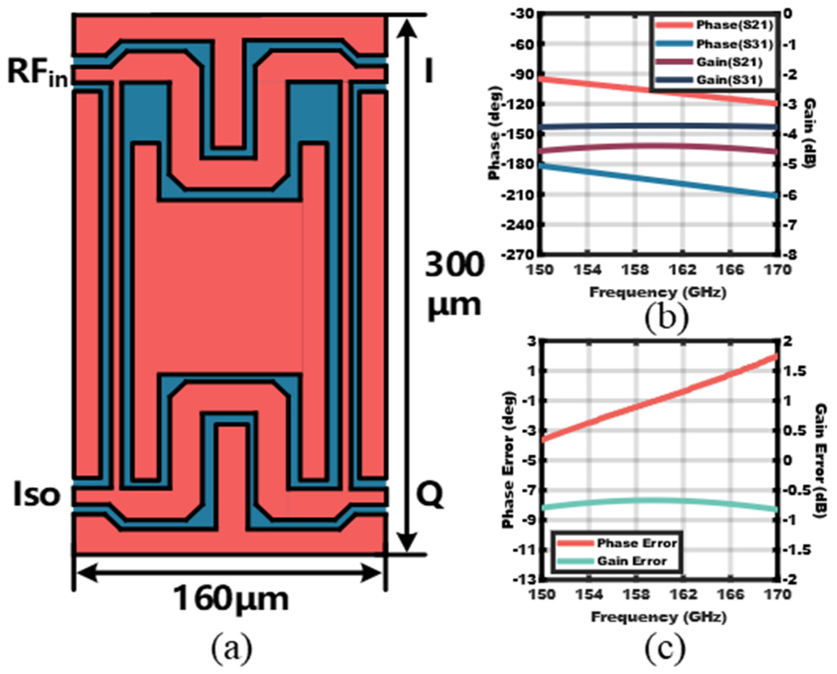
2.5. The Quadrature (90°) Hybrid
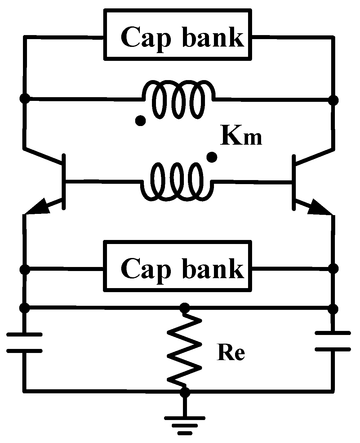
2.6. The Marchand Balun
3. Experimental Result
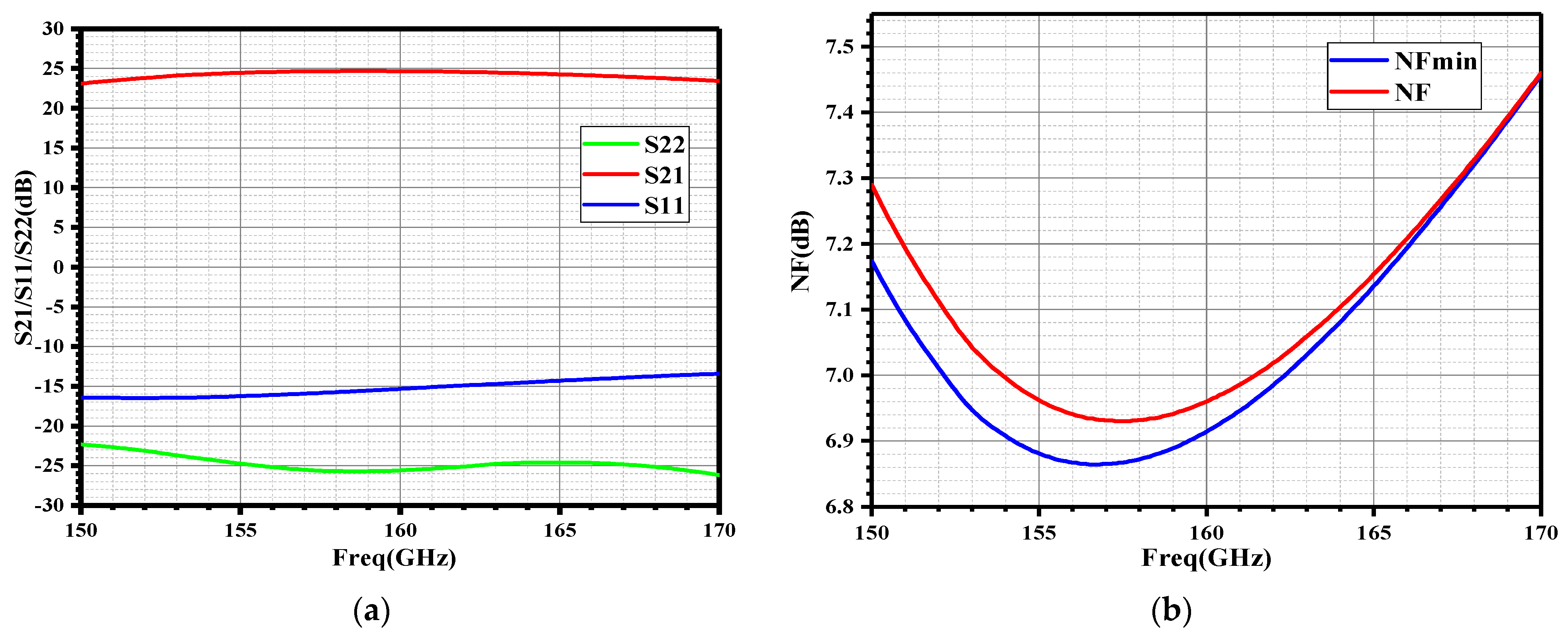
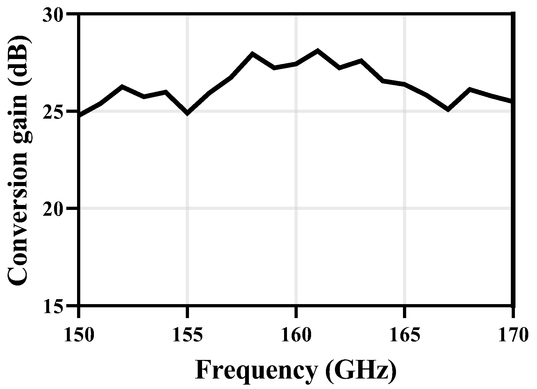
3.1. The Conversion Gain
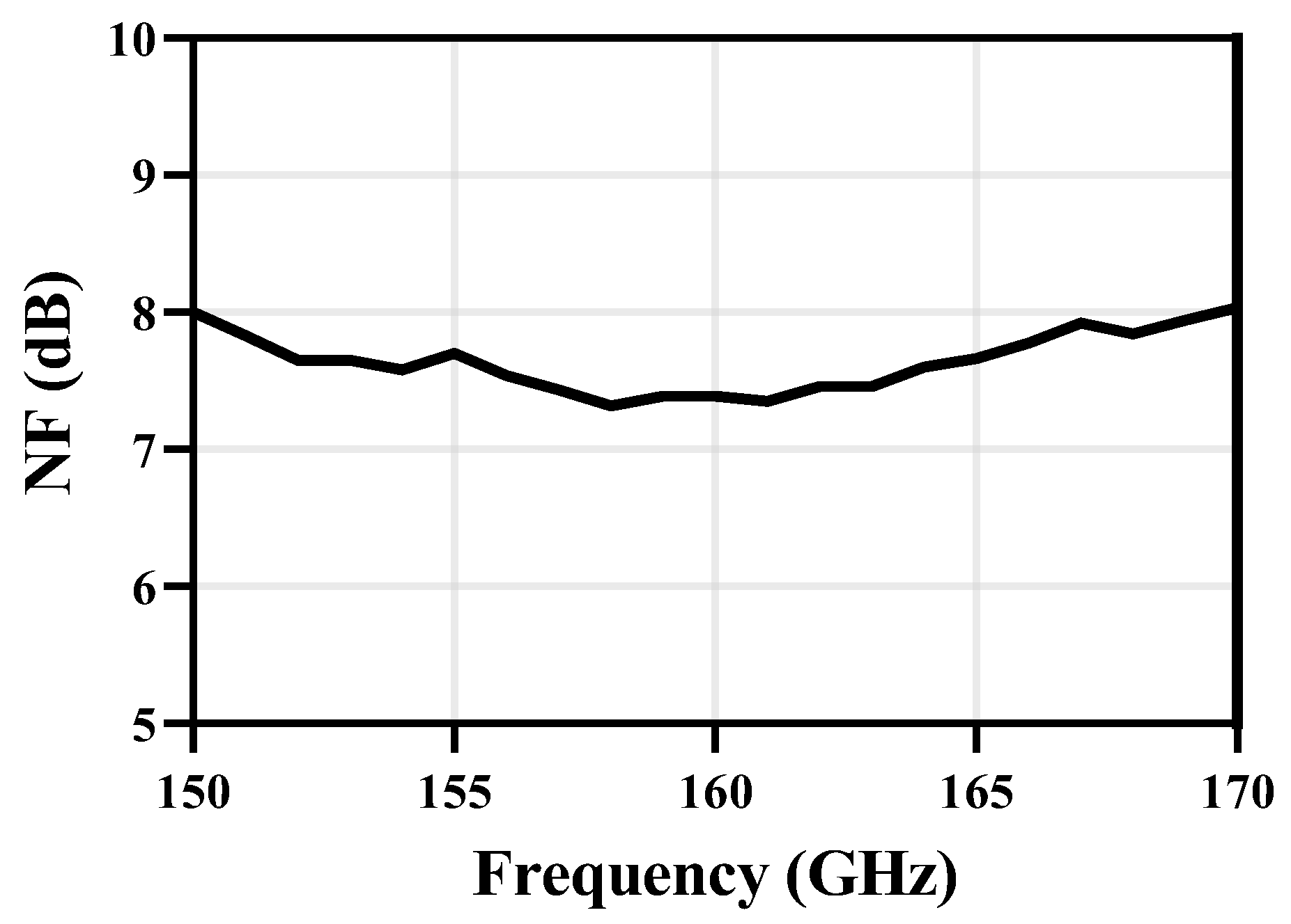
3.2. NF
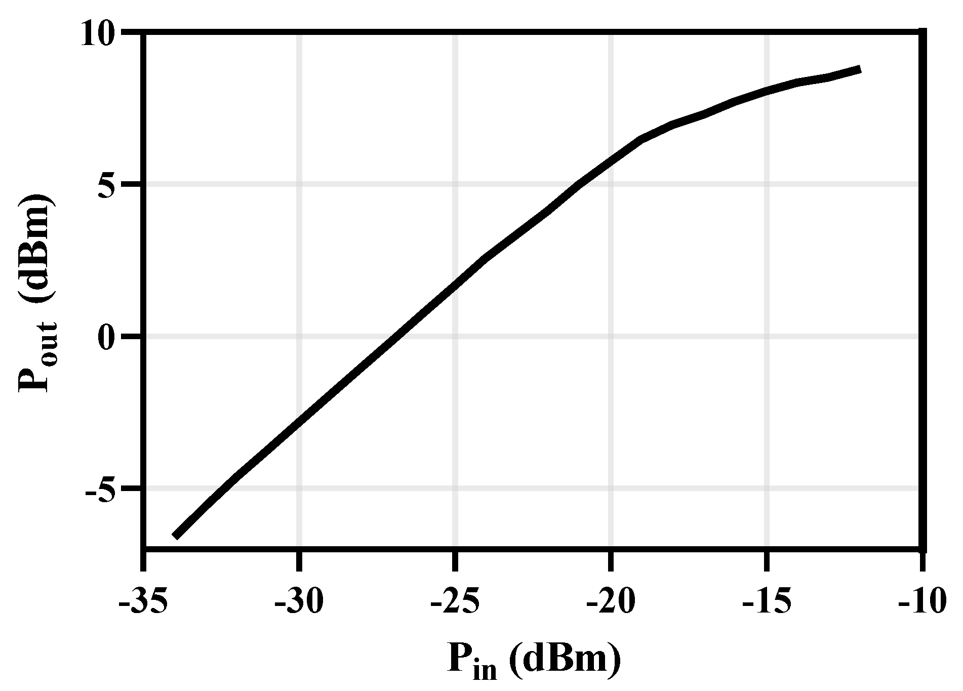
3.3. 1-dB Compression Point
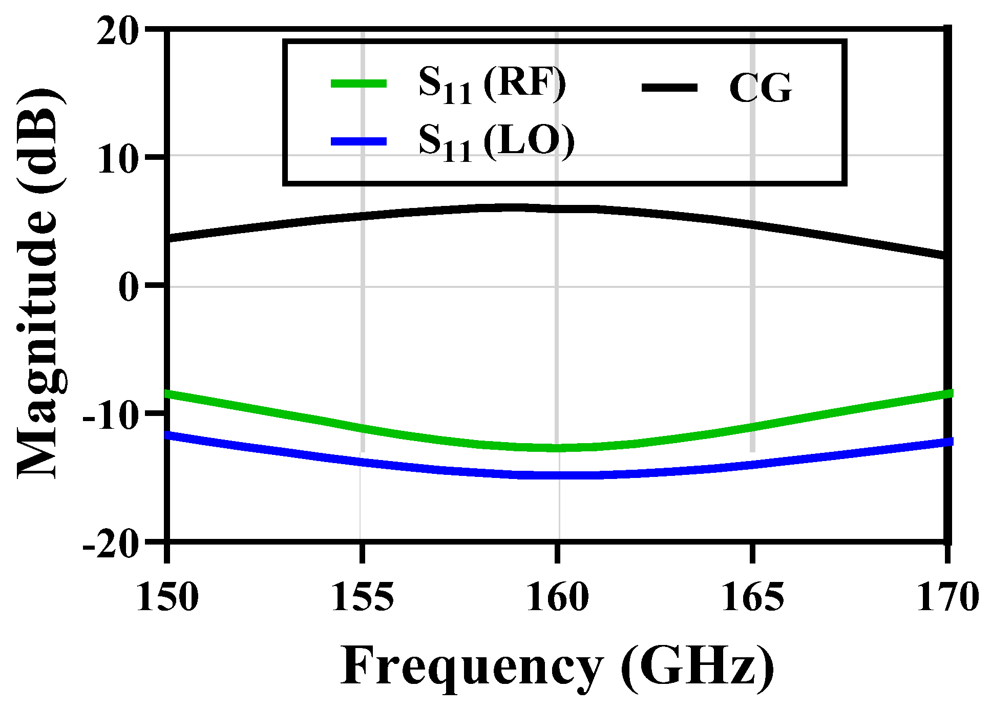
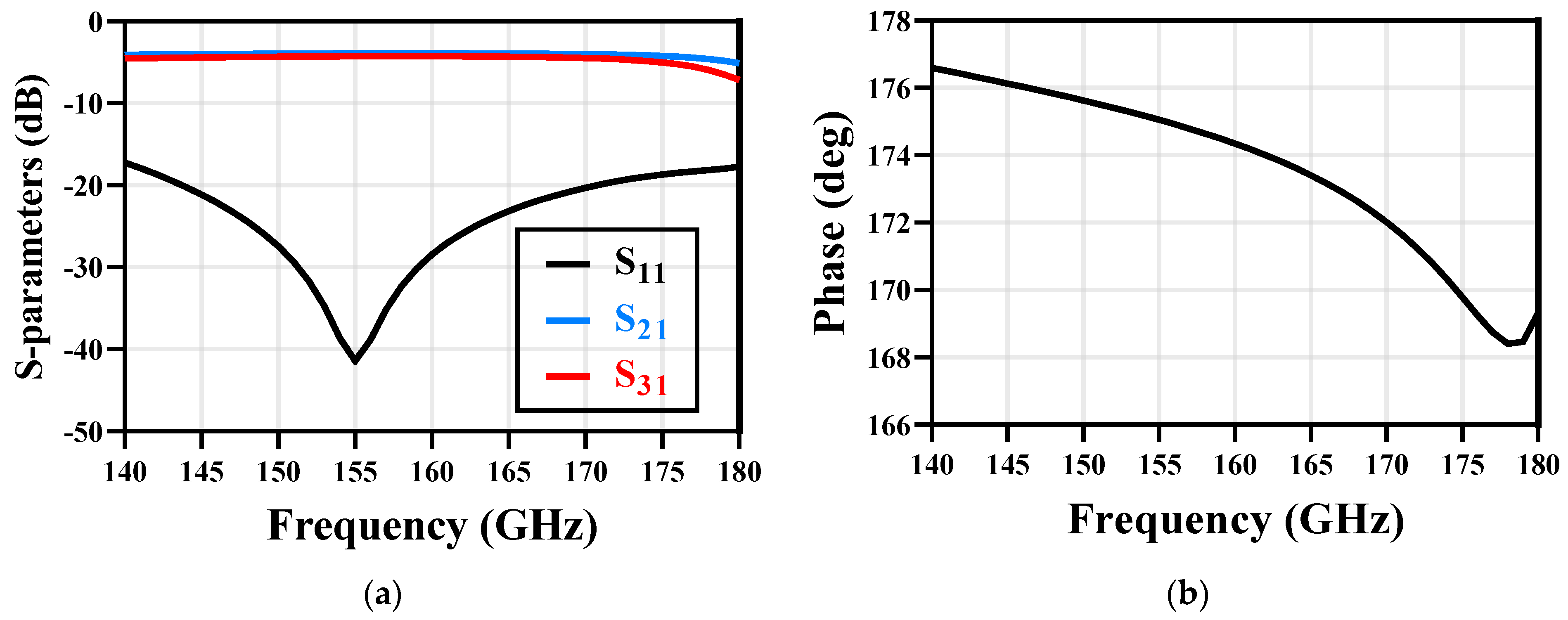
3.4. S-Parameters
4. Conclusions
Author Contributions
Funding
Informed Consent Statement
Data Availability Statement
Acknowledgments
Conflicts of Interest
References
- Chen, Z.; Ma, X.; Zhang, B.; Zhang, Y.; Niu, Z.; Kuang, N.; Li, S. A survey on terahertz communications. China Commun. 2019, 16, 1–35. [Google Scholar] [CrossRef]
- Akyildiz, I.F.; Han, C.; Hu, Z.; Nie, S.; Jornet, J.M. Terahertz Band Communication: An Old Problem Revisited and Research Directions for the Next Decade. IEEE Trans. Commun. 2022, 70, 4250–4285. [Google Scholar] [CrossRef]
- Guan, S.; Cheng, J.; Chang, S. Recent Progress of Terahertz Spatial Light Modulators: Materials, Principles and Applications. Micromachines 2022, 13, 1637. [Google Scholar] [CrossRef] [PubMed]
- Lin, C.-H.; Cheng, Y.-H. A THz Waveguide Bandpass Filter Design Using an Artificial Neural Network. Micromachines 2022, 13, 841. [Google Scholar] [CrossRef]
- Song, R.; Li, N. High Speed Terahertz Communication in the Space and Terrestrial Integrated Next Generation Wireless Communication Systems. In Proceedings of the 2020 13th UK-Europe-China Workshop on Millimetre-Waves and Terahertz Technologies (UCMMT), Online, 29–31 August 2020; pp. 1–3. [Google Scholar] [CrossRef]
- Stanko, S.; Caris, M.; Wahlen, A.; Sommer, R.; Wilcke, J.; Leuther, A.; Tessmann, A. Millimeter resolution with radar at lower terahertz. In Proceedings of the 2013 14th International Radar Symposium (IRS), Dresden, Germany, 19–21 June 2013; pp. 235–238. [Google Scholar]
- Kanno, A.; Sekine, N.; Uzawa, Y.; Hosako, I.; Kawanishi, T. 300-GHz versatile transceiver front-end for both communication and imaging. In Proceedings of the 2015 40th International Conference on Infrared, Millimeter, and Terahertz waves (IRMMW-THz), Hong Kong, China, 23–28 August 2015; pp. 1–2. [Google Scholar] [CrossRef]
- Kang, S.; Thyagarajan, S.V.; Niknejad, A.M. A 240 GHz Fully Integrated Wideband QPSK Transmitter in 65 nm CMOS. IEEE J. Solid-State Circuits 2015, 50, 2256–2267. [Google Scholar] [CrossRef]
- Wang, Z.; Chiang, P.Y.; Nazari, P.; Wang, C.C.; Chen, Z.; Heydari, P. A CMOS 210-GHz Fundamental Transceiver with OOK Modulation. IEEE J. Solid-State Circuits 2014, 49, 564–580. [Google Scholar] [CrossRef]
- Heinemann, B.; Barth, R.; Bolze, D.; Drews, J.; Fischer, G.G.; Fox, A.; Fursenko, O.; Grabolla, T.; Haak, U.; Knoll, D.; et al. SiGe HBT technology with fT/fmax of 300GHz/500GHz and 2.0 ps CML gate delay. In Proceedings of the 2010 International Electron Devices Meeting, San Francisco, CA, USA, 6–8 December 2010; pp. 30.5.1–30.5.4. [Google Scholar] [CrossRef]
- Chevalier, P.; Jungemann, C.; Lovblom, R.; Maneux, C.; Ostinelli, O.; Pawlak, A.; Rinaldi, N.; Rucker, H.; Wedel, G.; Zimmer, T.; et al. Si/SiGe:C and InP/GaAsSb Heterojunction Bipolar Transistors for THz Applications. Proc. IEEE 2017, 105, 1035–1050. [Google Scholar] [CrossRef]
- Aguilar, E.; Issakov, V.; Weigel, R. Highly-Integrated <0.14mm2D -Band Receiver Front-Ends for Radar and Imaging Applications in a 130 nm SiGe BiCMOS Technology. In Proceedings of the 2019 IEEE 19th Topical Meeting on Silicon Monolithic Integrated Circuits in RF Systems (SiRF), Orlando, FL, USA, 20–23 January 2019; pp. 1–4. [Google Scholar] [CrossRef]
- Carpenter, S.; Zirath, H.; He, Z.S.; Bao, M. A fully integrated D-band direct-conversion I/Q transmitter and receiver chipset in SiGe BiCMOS technology. J. Commun. Netw. 2021, 23, 73–82. [Google Scholar] [CrossRef]
- Farid, A.A.; Simsek, A.; Ahmed, A.S.H.; Rodwell, M.J.W. A Broadband Direct Conversion Transmitter/Receiver at D-band Using CMOS 22nm FDSOI. In Proceedings of the 2019 IEEE Radio Frequency Integrated Circuits Symposium (RFIC), Boston, MA, USA, 2–4 June 2019; pp. 135–138. [Google Scholar] [CrossRef]
- Wang, C.; Rebeiz, G. A 2-Channel 136–156 GHz Dual Down-Conversion I/Q Receiver with 30 dB Gain and 9.5 dB NF Using CMOS 22 nm FDSOI. In Proceedings of the 2021 IEEE Radio Frequency Integrated Circuits Symposium (RFIC), San Diego, CA, USA, 11–13 June 2021; pp. 219–222. [Google Scholar] [CrossRef]
- Kim, J.; Buckwalter, J.F. Staggered Gain for 100+ GHz Broadband Amplifiers. IEEE J. Solid-State Circuits 2011, 46, 1123–1136. [Google Scholar] [CrossRef]
- Jang, T.H.; Jung, K.P.; Kang, J.S.; Byeon, C.W.; Park, C.S. 120-GHz 8-Stage Broadband Amplifier with Quantitative Stagger Tuning Technique. IEEE Trans. Circuits Syst. I: Regul. Pap. 2020, 67, 785–796. [Google Scholar] [CrossRef]
- Karakuzulu, A.; Eissa, M.H.; Kissinger, D.; Malignaggi, A. A Broadband 110–170-GHz Stagger-Tuned Power Amplifier With 13.5-dBm Psat in 130-nm SiGe. IEEE Microw. Wirel. Compon. Lett. 2021, 31, 56–59. [Google Scholar] [CrossRef]
- Turkmen, E.; Burak, A.; Guner, A.; Kalyoncu, I.; Kaynak, M.; Gurbuz, Y. A SiGe HBT D-Band LNA With Butterworth Response and Noise Reduction Technique. IEEE Microw. Wirel. Compon. Lett. 2018, 28, 524–526. [Google Scholar] [CrossRef]
- Turkmen, E.; Aksoyak, I.K.; Debski, W.; Winkler, W.; Ulusoy, A.Ç. A 225–265 GHz I-Q Receiver in 130-nm SiGe BiCMOS for FMCW Radar Applications. IEEE Microw. Wirel. Compon. Lett. 2022, 32, 899–902. [Google Scholar] [CrossRef]
- Liu, X.; Luong, H.C. A 170-GHz 23.7% Tuning-Range CMOS Injection-Locked LO Generator with Third-Harmonic Enhancement. IEEE Trans. Microw. Theory Tech. 2020, 68, 2668–2678. [Google Scholar] [CrossRef]
- Chen, A.C.; Pham, A.-V.; Leoni, R.E., III. A Novel Broadband Even-Mode Matching Network for Marchand Baluns. IEEE Trans. Microw. Theory Tech. 2009, 57, 2973–2980. [Google Scholar] [CrossRef]


| This Work | [12] | [13] | [14] | [15] | |
|---|---|---|---|---|---|
| Technology | 130 nm SiGe | 130 nm SiGe | 130 nm SiGe | 22 nm SOI | 22 nm SOI |
| ft/fmax [GHz] | 300/450 | 250/370 | 230/280 | 240/230 | 240/230 |
| f3dB[GHz] | 150–170 | 114–146 | 112–140 | 125–145 | 140–147 |
| LO generation | X9 multiplier chain | Off-chip | X6 multiplier chain | X9 multiplier chain | X3 multiplier chain |
| P1dB (input) [dBm] | −19# | −7 | −24 | −30 | −29 |
| CG [dB] | 28# | 25 | 27 | 27 | 27–30 |
| NF [dB] | 7.3 * | 11.8 * | 10 * | 8.5 * | 9 |
| PDC [mW] | 428 | 326 | 280 | 198 | 197.5 |
| Area [mm2] | 1.04 | 0.1 | 1.54 | 1.44 | 3.1 |
Disclaimer/Publisher’s Note: The statements, opinions and data contained in all publications are solely those of the individual author(s) and contributor(s) and not of MDPI and/or the editor(s). MDPI and/or the editor(s) disclaim responsibility for any injury to people or property resulting from any ideas, methods, instructions or products referred to in the content. |
© 2022 by the authors. Licensee MDPI, Basel, Switzerland. This article is an open access article distributed under the terms and conditions of the Creative Commons Attribution (CC BY) license (https://creativecommons.org/licenses/by/4.0/).
Share and Cite
He, F.; Ding, Y.; Xu, Z.; Ni, M.; Tian, Y.; Zhang, Z.; Shi, Z.; Wang, K.; Xie, Q.; Wang, Z. A D-Band Direct-Conversion IQ Receiver with 28 dB CG and 7.3 dB NF in 130 nm SiGe Process. Micromachines 2023, 14, 87. https://doi.org/10.3390/mi14010087
He F, Ding Y, Xu Z, Ni M, Tian Y, Zhang Z, Shi Z, Wang K, Xie Q, Wang Z. A D-Band Direct-Conversion IQ Receiver with 28 dB CG and 7.3 dB NF in 130 nm SiGe Process. Micromachines. 2023; 14(1):87. https://doi.org/10.3390/mi14010087
Chicago/Turabian StyleHe, Fei, Yuhan Ding, Zhongchen Xu, Menghu Ni, Yibo Tian, Zhenyi Zhang, Zhixiang Shi, Kailei Wang, Qian Xie, and Zheng Wang. 2023. "A D-Band Direct-Conversion IQ Receiver with 28 dB CG and 7.3 dB NF in 130 nm SiGe Process" Micromachines 14, no. 1: 87. https://doi.org/10.3390/mi14010087
APA StyleHe, F., Ding, Y., Xu, Z., Ni, M., Tian, Y., Zhang, Z., Shi, Z., Wang, K., Xie, Q., & Wang, Z. (2023). A D-Band Direct-Conversion IQ Receiver with 28 dB CG and 7.3 dB NF in 130 nm SiGe Process. Micromachines, 14(1), 87. https://doi.org/10.3390/mi14010087