Abstract
In this work, we successfully demonstrated In0.53Ga0.47As/InAs/In0.53Ga0.47As composite channel metamorphic high electron mobility transistors (mHEMTs) on a GaAs substrate. The fabricated mHEMTs with a 100 nm gate length exhibited excellent DC and logic characteristics such as VT = −0.13 V, gm,max = 949 mS/mm, subthreshold swing (SS) = 84 mV/dec, drain-induced barrier lowering (DIBL) = 89 mV/V, and Ion/Ioff ratio = 9.8 × 10³ at a drain-source voltage (VDS) = 0.5 V. In addition, the device exhibited excellent high-frequency characteristics, such as fT/fmax = 261/304 GHz for the measured result and well-matched modeled fT/fmax = 258/309 GHz at VDS = 0.5 V, which is less power consumption compared to other material systems. These high-frequency characteristics are a well-balanced demonstration of fT and fmax in the mHEMT structure on a GaAs substrate.
1. Introduction
High electron mobility transistors (HEMTs) based on indium-rich InxGa1-xAs channel materials on an InP substrate have demonstrated excellent high-frequency and logic characteristics. In terms of high-frequency characteristics of the InGaAs channel HEMT, H. -B. Jo et al. demonstrated 738 GHz unity current gain cutoff frequency (fT) in a 19 nm In0.8Ga0.2As composite-channel HEMT on a InP substrate [1], D. -H. Kim et al. showed excellent logic performance and a fT of 644 GHz in 30 nm InAs Pseudomorphic HEMTs (pHEMTs) [2], and Northrop Grumman Corporation exhibited an fT of 610 GHz/fmax of 1.5 THz by using an In0.53GaAs/InAs/In0.53GaAs composite channel with a Lg of 25 nm [3]. These remarkable performances have been achieved through downscaling of device feature size, an optimized fabrication process, and optimized InGaAs channel materials for excellent transport properties. In addition, InGaAs channel MOSFETs have shown outstanding logic performance on various substrates, such as InP and flexible substrates, with extensive efforts to enhance their capability in new device structures, S/D Ohmic contacts, and optimization of the gate stack [4,5,6,7]. Meanwhile, large-size and cheaper-cost substrates will be essential for large-volume manufacturing from a mass production point of view, but an InP substrate is more expensive than a GaAs substrate, and the size to date is limited to 6 inches. To overcome these limitations of the InP substrate, many groups have demonstrated many outstanding results for mHEMTs on a GaAs substrate [8,9,10,11]. In particular, Teledyne demonstrated excellent results of a 688 GHz fT by utilizing an In0.7GaAs mHEMT structure with dual Si δ-doping and an InAs-rich In0.7Al0.3As spacer on a GaAs substrate in 2011 [9]. Fraunhofer showed a maximum oscillation frequency (fmax) exceeding 1000 GHz by using an In0.8GaAs mHEMT structure on a GaAs substrate in 2013 [11]. Among various HEMT structures, an InGaAs/InAs/InGaAs composite channel was used to enhance high-frequency characteristics in HEMT structures because of its excellent electron transport properties, such as electron velocity and mobility [2,3,12]. However, an In0.53Ga0.47As/InAs/In0.53Ga0.47As composite channel structure on a GaAs substrate has not been demonstrated yet. In this work, we fabricated an In0.53Ga0.47As/InAs/In0.53Ga0.47As composite channel HEMT on a GaAs substrate incorporating a molybdenum (Mo)-based Ohmic contact using blanket Mo deposition and investigated its electrical performance, such as DC, logic, and RF characteristics, with an Lg of 100 nm.
2. Layer Structure and Experiments
The mHEMT heterostructures consisted of a 500 nm In0.52Al0.48As buffer, a 12 nm In0.53Ga0.47As/InAs/In0.53Ga0.47As (4/5/3 nm) channel, a 3 nm In0.52Al0.48As spacer, Si δ-doping (4.1 × 1012 cm−2), an 8 nm In0.52Al0.48As barrier, a 4 nm InP etch stop layer, and a 35 nm heavily doped In0.53Ga0.47As/In0.52Al0.48As multi-layer cap from the bottom to the top as shown in Figure 1a. The energy band diagram of the epitaxial structure is shown in Figure 1b. From this structure, sheet carrier density and electron hall mobility were measured to be 2.92 × 1012 cm−2 and 10,000 cm2/V·s at room temperature, respectively, with four-point probe measurement methods (Van der Pauw measurement method). Device fabrication began with a 30 nm blanket molybdenum (Mo) deposition for ohmic contact to prevent surface contamination and improve the contact resistance (Rc), then mesa isolation down to an InAlAs buffer layer by Mo dry etching and wet etching. After Ti/Au/Ni (20/150/30 nm) metallization for source and drain, dry etching in an SF6/Ar plasma was performed to etch Mo in the gate region using the Ni metal etch mask of the source and drain [13]. A 30 nm thick layer of SiO2 was deposited by plasma-enhanced chemical vapor deposition (PECVD), and then the pad patterns with Ti/Au (20/300 nm) were defined for ground-signal-ground probing. After e-beam exposure, the defined e-beam resist pattern was transferred to define the T-gate by using reactive ion etching based on CF4 plasma. Gate recessing was performed in two different step stages, followed by anisotropic reactive ion etching of the InP etch stop layer in an Ar-based plasma [14]. After InP etching, Schottky gate metallization of Ti/Pt/Au (20/30/300 nm) was deposited on top of the InAlAs layer. Finally, the mHEMT with a width of 2 × 50 µm was fabricated, and a schematic of the fabricated mHEMT is shown in Figure 1c. Figure 1d shows the SEM image of the fabricated t-gate, whose foot and head sizes are 100 nm and 470 nm, respectively.
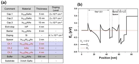
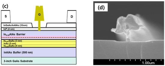
Figure 1.
(a) Epitaxial structure of the In0.53Ga0.47As/InAs/In0.53Ga0.47As composite channel HEMT structure on a GaAs substrate. (b) Energy band diagram of the epitaxial structure (c) Schematic of the In0.53Ga0.47As/InAs/In0.53Ga0.47As composite channel HEMT on a GaAs substrate (d) SEM image of the fabricated T-gate.
3. Results and Discussion
The transfer characteristic and output characteristic of the mHEMTs are shown in Figure 2. The maximum transconductance (gm,max) and maximum drain current density (ID,max) were 949 mS/mm and 413 mA/mm at VDS = 0.5 V, respectively. The output characteristics presented in Figure 2b show good pinch-off characteristics, but the measured Ron was 733 Ω-μm, which is a higher value than the lift-off Mo/Ti/Mo/Au metal scheme with an InAs rich InAlAs barrier spacer [15]. The ohmic contact resistance (Rc) and sheet resistance (Rsh) measured by the transmission line method (TLM) was as low as 0.01 Ω-mm and 75.5 Ω/sq as shown in Figure 2c. When compared to the lift-off method using a Mo/Ti//Mo/Au scheme (30/20/20/150 nm) on the same multi-cap layer, the blanket Mo method shows a higher Rsh value of 75.5 Ω/sq than the lift-off method of 69.2 Ω/sq because of SF6/Ar plasma damage in the active region during Mo etching to define the active gate region. However, the blanket Mo method shows a Rc of 0.011 Ohm-mm, which is lower than that of 0.026 Ohm-mm with the lift-off method because it is beneficial to protect the surface underneath the metal contact region from contaminants during the device process. Due to the lower Rc of the Mo blanket method, a lower Ron value could be achieved if the S/D distance was reduced, as in the self-aligned gate scheme.
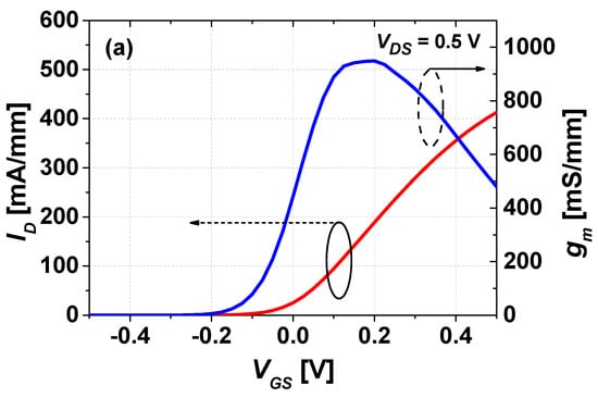
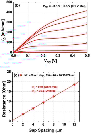
Figure 2.
(a) Typical transfer characteristics of the mHEMTs measured at VDS = 0.5 V. (b) Typical output characteristics of the mHEMTs (VGS = −0.5 V ~ 0.5 V). (c) TLM result of the Mo-based Ohmic contact.
Figure 3 shows the subthreshold characteristics at VDS = 0.5 V and 0.05 V, respectively. At VDS = 0.5 V, the threshold voltage (VT) is −0.13 V, defined as the value of VGS that yields at ID = 1 mA/mm, and a VT of −0.13 V indicates that the fabricated mHEMT operated in depletion mode (D-mode). The fabricated device shows excellent electrostatic integrity, such as the subthreshold swing (SS) of 84 mV/dec, the drain-induced barrier lowering (DIBL) of 89 mV/V, and the Ion/Ioff ratio of 9.8 × 10³, respectively. Additionally, the gate leakage current of the fabricated mHEMT was measured at VDS = 0.5 V and shows that the gate Schottky metallization is in good contact with the In0.52Al0.48As barrier layer. These outstanding logic performances are due to the well-designed heterostructure and optimized fabrication process on the GaAs substrate.
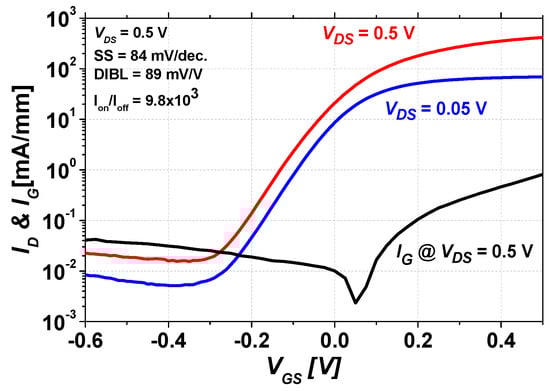
Figure 3.
Subthreshold characteristics of the mHEMT were measured at VDS = 0.5 V and VDS = 0.05 V, and the gate leakage current was measured at VDS = 0.5 V, respectively.
To verify the high-frequency RF characteristics of the mHEMT, S-parameters were measured from 0.5 to 40 GHz using a vector network analyzer (VNA). In addition, small-signal modeling was performed by using a small-signal equivalent circuit [16], and we found that small-signal modeling and measured S-parameters are well matched, as shown in Figure 4a. Figure 4b shows the unity current gain cutoff frequency (fT), maximum oscillation frequency (fmax), and maximum stable gain (MSG)/maximum available gain (MAG) against frequency for the measured results (symbols) and modeled results (solid lines) at VDS = 0.5 V and VGS = 0.2 V with a Lg of 100 nm mHEMT device. The de-embedding method was done by using open and short patterns to extract parasitic pad capacitance and inductance. We obtained 261 GHz/304 GHz for fT/fmax by extrapolation (dashed lines) and 258 GHz/309 GHz for fT/fmax by small-signal modeling, respectively. This excellent high-frequency response is due to the high value of the intrinsic transconductance (gmi) of 2.0 mS/µm. The extracted intrinsic parameters of the mHEMT are summarized in Table 1 and are well-matched to the measured results. The difference between gm,ext (0.95 mS/µm) and gmi (2.0 mS/µm) is due to the Rs and go values according to equation (1) [17].
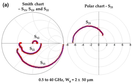
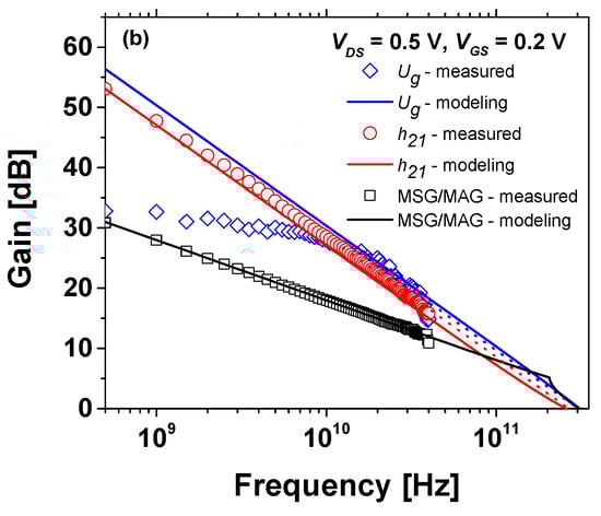
Figure 4.
(a) Comparison of small-signal modeling and measured S-parameters at VDS = 0.5 V and VGS = 0.2 V. A Smith chart of S11, S12, and S22 (left) and a polar chart of S12 (right). (b) Measured (symbols) and modeled (solid lines) of RF gains-Maximum oscillation frequency (fmax), maximum stable gain (MSG)/maximum available gain (MAG), and unity current gain cutoff frequency (fT) of the mHEMTs at VDS = 0.5 V and VGS = 0.2 V.

Table 1.
Extracted intrinsic small-signal parameters.
Figure 5 shows fT and fmax as functions of ID at VDS = 0.5 V and 0.4 V. Around an ID of 75 mA/mm, our device had already exhibited an fT and fmax value of over 200 GHz and was confirmed to operate stably for the fabricated mHEMT.
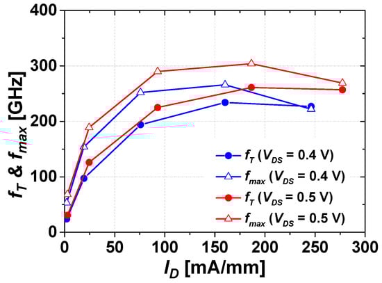
Figure 5.
Maximum oscillation frequency (fmax) and unity current gain cutoff frequency (fT) of the mHEMTs against drain current density (ID) at a VDS = 0.5 and 0.4 V, respectively.
Table 2 shows the benchmark high-frequency characteristics of the published state-of-the-art pHEMT and mHEMT results with an Lg of 100 nm. Among various HEMT structures, the In0.53Ga0.47As/InAs/In0.53Ga0.47As composite channel HEMT on an InP substrate shows excellent high-frequency characteristics such as an fT of 421 GHz and an fmax of 620 GHz because of the well-optimized fabrication process and improved carrier transport properties of the In0.53Ga0.47As/InAs/In0.53Ga0.47As composite channel [18]. Our fabricated mHEMT exhibits an excellent LgfT of 26.1 GHz-µm, which is related to carrier transport properties [19], and an outstanding fT/fmax of 261/304 GHz with a Lg of 100 nm at a VDS = 0.5 V. Although the performance of the fabricated mHEMT is not comparable to that of the In0.53Ga0.47As/InAs/In0.53Ga0.47As composite channel HEMT on an InP substrate, our fabricated mHEMT shows outstanding high-frequency characteristics compared to a single InGaAs channel HEMT on an InP substrate and other mHEMT structures because of the excellent transport properties of the composite channel on a GaAs substrate. Additionally, our fabricated device is operated at a VDS = 0.5 V, which has a lower power consumption than other group devices’ operational voltage. These excellent performances are mainly attributed to the well-grown In0.53Ga0.47As/InAs/In0.53Ga0.47As composite channel structure by using an In0.52AlAs buffer layer on a GaAs substrate, and a fabricated mHEMT would be a good candidate for the high-frequency device in both 5G and 6G communications through further scaling-down of device feature size.
Table 2.
Performance parameters of the pHEMTs and mHEMTs with a Lg of 100 nm.
4. Conclusions
The 100 nm In0.53Ga0.47As/InAs/In0.53Ga0.47As composite channel metamorphic high electron mobility transistors (mHEMTs) on a GaAs substrate exhibited excellent logic characteristics as well as high-frequency RF performances. These outstanding performances are due to the excellent carrier transport properties of the well-grown In0.53Ga0.47As/InAs/In0.53Ga0.47As composite channel mHEMT structure on a GaAs substrate and an optimized fabrication process. The proposed mHEMT structure on a GaAs substrate, together with optimized source/drain and gate technologies, will potentially improve logic and high-frequency characteristics. Furthermore, the proposed mHEMT structure grown on a large-size GaAs substrate could be indispensable for large-volume manufacturing.
Author Contributions
Conceptualization, S.H.S. and J.-H.J.; methodology, S.H.S., H.J. and J.-P.S.; validation, S.H.S., H.J. and J.-P.S.; formal analysis, S.H.S. and J.-P.S.; investigation, S.H.S., H.J. and J.-P.S.; resources, S.H.S. and J.-H.J.; data curation, S.H.S. and J.-P.S.; writing—original draft preparation, S.H.S., H.J. and J.-P.S.; writing—review and editing, S.H.S. and J.-P.S.; visualization, S.H.S. and J.-P.S.; supervision, S.H.S. and J.-H.J.; funding acquisition, S.H.S. and J.-P.S. All authors have read and agreed to the published version of the manuscript.
Funding
This research was supported by the National R&D Program through the National Research Foundation of Korea (NRF), funded by the Ministry of Science and ICT (2022M3I8A1078437), and the Nanomaterial Technology Development Program through the National Research Foundation of Korea (NRF), funded by the Ministry of Science, ICT, and Future Planning (2009-0082580).
Conflicts of Interest
The authors declare no conflict of interest. The funders had no role in the design of the study; in the collection, analyses, or interpretation of data; in the writing of the manuscript; or in the decision to publish the results.
References
- Jo, H.-B.; Yun, S.-W.; Kim, J.-G.; Yun, D.-Y.; Lee, I.-G.; Kim, D.-H.; Kim, T.-W.; Kim, S.-K.; Yun, J.; Kim, T.; et al. Lg = 19 nm In0.8Ga0.2As composite-channel HEMTs with ft = 738 GHz and fmax = 492 GHz. In Proceedings of the 2020 IEEE International Electron Devices Meeting (IEDM), San Francisco, CA, USA, 12–18 December 2020. [Google Scholar]
- Kim, D.-H.; del Alamo, J.A. 30-nm InAs PHEMTs With fT = 644 GHz and fmax = 681 GHz. IEEE Electron Device Lett. 2010, 31, 806–808. [Google Scholar]
- Mei, X.; Yoshida, W.; Lange, M.; Lee, J.; Zhou, J.; Liu, P.-H.; Leong, K.; Zamora, A.; Padilla, J.; Sarkozy, S.; et al. First Demonstration of amplification at 1 THz using 25-nm InP high electron mobility transistor process. IEEE Electron Device Lett. 2015, 36, 327–329. [Google Scholar] [CrossRef]
- Shin, C.-S.; Park, W.-K.; Shin, S.H.; Cho, Y.D.; Ko, D.H.; Kim, T.-W.; Koh, D.H.; Kwon, H.M.; Hill, R.J.; Kirsch, P.; et al. Sub-100 nm regrown S/D gate-last In0.7Ga0.3As QW MOSFETs with μn, eff > 5,500 cm2/v-S. In Proceedings of the 2014 Symposium on VLSI Technology (VLSI-Technology): Digest of Technical Papers, Honolulu, HI, USA, 9–12 June 2014. [Google Scholar]
- Jo, H.-B.; Lee, I.-G.; Baek, J.-M.; Lee, S.T.; Choi, S.-M.; Kim, H.-J.; Jeong, H.-S.; Park, W.-S.; Yoo, J.; Lee, H.-Y.; et al. Lg = 130 nm GAA MBCFETs with three-level stacked In0.53Ga0.47As nanosheets. In Proceedings of the 2022 IEEE Symposium on VLSI Technology and Circuits (VLSI Technology and Circuits), Honolulu, HI, USA, 12–17 June 2022. [Google Scholar]
- Kim, T.-W.; Kim, D.-H.; Koh, D.H.; Kwon, H.M.; Baek, R.H.; Veksler, D.; Huffman, C.; Matthews, K.; Oktyabrsky, S.; Greene, A.; et al. Sub-100 nm InGaAs quantum-well (QW) tri-gate MOSFETs with Al2O3/HfO2 (EOT < 1 nm) for low-power logic applications. In Proceedings of the 2013 IEEE International Electron Devices Meeting, Washington, DC, USA, 9–11 December 2013. [Google Scholar]
- Park, S.; Kim, D.-K.; Cho, Y.-D.; Shim, J.-P.; Shin, C.-S.; Shin, S.H. Demonstration of high performance flexible In0.7Ga0.3As MOSFETs using liquid polyimide (LPI) transfer. IEEE Electron Device Lett. 2022, 43, 858–861. [Google Scholar] [CrossRef]
- Leuther, A.; Weber, R.; Dammann, M.; Schlechtweg, M.; Mikulla, M.; Walther, M.; Weimann, G. Metamorphic 50 nm InAs-channel HEMT. In Proceedings of the International Conference on Indium Phosphide and Related Materials, Glasgow, UK, 8–12 May 2005. [Google Scholar]
- Kim, D.-H.; Brar, B.; del Alamo, J.A. Ft = 688 GHz and Fmax = 800 GHz in Lg = 40 nm In0.7Ga0.3As MHEMTs with Gm_max > 2.7 ms/µm. In Proceedings of the 2011 International Electron Devices Meeting, Washington, DC, USA, 5–7 December 2011. [Google Scholar]
- Komiak, J.J.; Smith, P.M.; Duh, K.H.; Xu, D.; Chao, P.C. Metamorphic HEMT technology for microwave, millimeter-wave, and submillimeter-wave applications. In Proceedings of the 2013 IEEE Compound Semiconductor Integrated Circuit Symposium (CSICS), Monterey, CA, USA, 13–16 October 2013. [Google Scholar]
- Leuther, A.; Tessmann, A.; Dammann, M.; Massler, H.; Schlechtweg, M.; Ambacher, O. 35 nm mHEMT technology for THz and Ultra Low Noise Applications. In Proceedings of the 2013 International Conference on Indium Phosphide and Related Materials (IPRM), Kobe, Japan, 19–23 May 2013. [Google Scholar]
- Akazaki, T.; Arai, K.; Enoki, T.; Ishii, Y. Improved InAlAs/InGaAs HEMT characteristics by inserting an InAs layer into the InGaAs channel. IEEE Electron Device Lett. 1992, 13, 325–327. [Google Scholar] [CrossRef]
- Baraskar, A.K.; Wistey, M.A.; Jain, V.; Singisetti, U.; Burek, G.; Thibeault, B.J.; Lee, Y.J.; Gossard, A.C.; Rodwell, M.J. Ultralow resistance, nonalloyed ohmic contacts to N-InGaAs. J. Vac. Sci. Technol. B Microelectron. Nanometer Struct. 2009, 27, 2036. [Google Scholar] [CrossRef]
- Suemitsu, T.; Yokoyama, H.; Ishii, T.; Enoki, T.; Meneghesso, G.; Zanoni, E. 30-nm two-step recess gate InP-based InAlAs/InGaAs HEMTs. IEEE Trans. Electron Devices 2002, 49, 1694–1700. [Google Scholar] [CrossRef]
- Kim, T.-W.; Kim, D.-H.; del Alamo, J.A. InGaAs HEMT with InAs-rich InAlAs barrier spacer for reduced source resistance. Electron. Lett. 2011, 47, 406. [Google Scholar] [CrossRef]
- Dambrine, G.; Cappy, A.; Heliodore, F.; Playez, E. A new method for determining the FET small-signal equivalent circuit. IEEE Trans. Microw. Theory Tech. 1988, 36, 1151–1159. [Google Scholar] [CrossRef]
- Yun, S.-W.; Kim, D.-H. Comprehensive study of components affecting extrinsic transconductance in In0.7Ga0.3As quantum-well high-electron-mobility transistors for image sensor applications. J. Sens. Sci. Technol. 2021, 30, 441–445. [Google Scholar] [CrossRef]
- Kim, D.-H.; Chen, P.; Kim, T.-W.; Urteaga, M.; Brar, B. LG = 100 nm InAs pHEMTs on InP substrate with record high frequency response. Electron. Lett. 2012, 48, 1352. [Google Scholar] [CrossRef]
- Geum, D.M.; Shin, S.H.; Kim, M.S.; Jang, J.H. 75 nm t-shaped gate for In0.17Al0.83N/GaN HEMTs with minimal short-channel effect. Electron. Lett. 2013, 49, 1536–1537. [Google Scholar] [CrossRef]
- Liu, L.; Alt, A.R.; Benedickter, H.; Bolognesi, C.R. InP-HEMT X-band low-noise amplifier with Ultralow 0.6-mW power consumption. IEEE Electron Device Lett. 2012, 33, 209–211. [Google Scholar] [CrossRef]
- Tessmann, A. 220-GHz metamorphic HEMT amplifier MMICS for high-resolution imaging applications. IEEE J. Solid-State Circuits 2005, 40, 2070–2076. [Google Scholar] [CrossRef]
- Lee, J.M.; Chang, W.J.; Kang, D.M.; Min, B.G.; Yoon, H.S.; Chang, S.J.; Jung, H.W.; Kim, W.; Jung, J.; Kim, J.; et al. W-band MMIC chipset in 0.1-um mHEMT technology. ETRI J. 2020, 42, 549–561. [Google Scholar] [CrossRef]
Disclaimer/Publisher’s Note: The statements, opinions and data contained in all publications are solely those of the individual author(s) and contributor(s) and not of MDPI and/or the editor(s). MDPI and/or the editor(s) disclaim responsibility for any injury to people or property resulting from any ideas, methods, instructions or products referred to in the content. |
© 2022 by the authors. Licensee MDPI, Basel, Switzerland. This article is an open access article distributed under the terms and conditions of the Creative Commons Attribution (CC BY) license (https://creativecommons.org/licenses/by/4.0/).