
Activation Enhancement and Grain Size Improvement for Poly-Si Channel Vertical Transistor by Laser Thermal Annealing in 3D NAND Flash
 ,
, 
Abstract
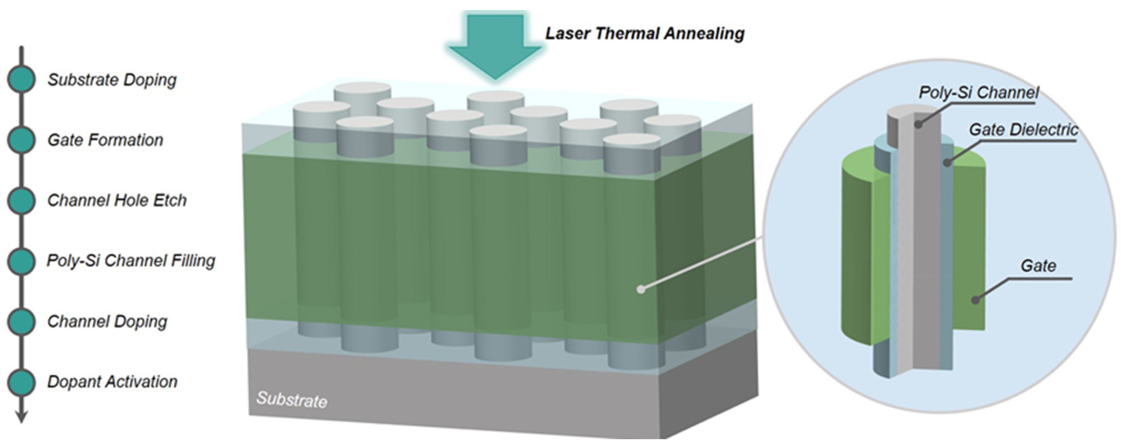
:1. Introduction
2. Experiments
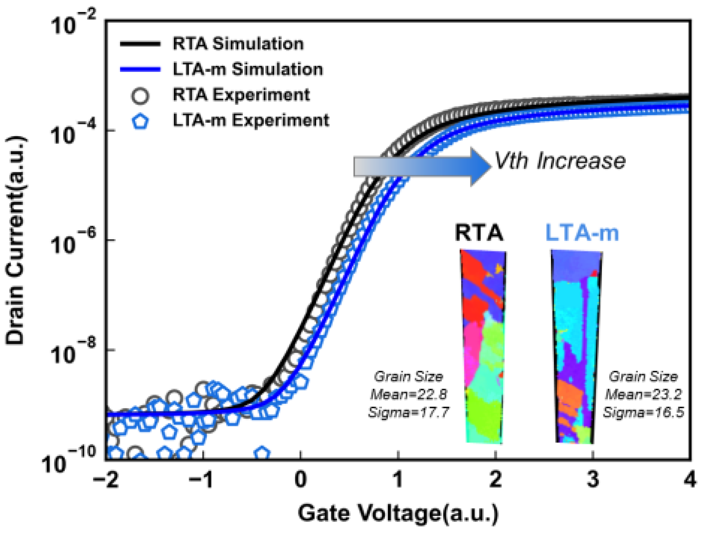
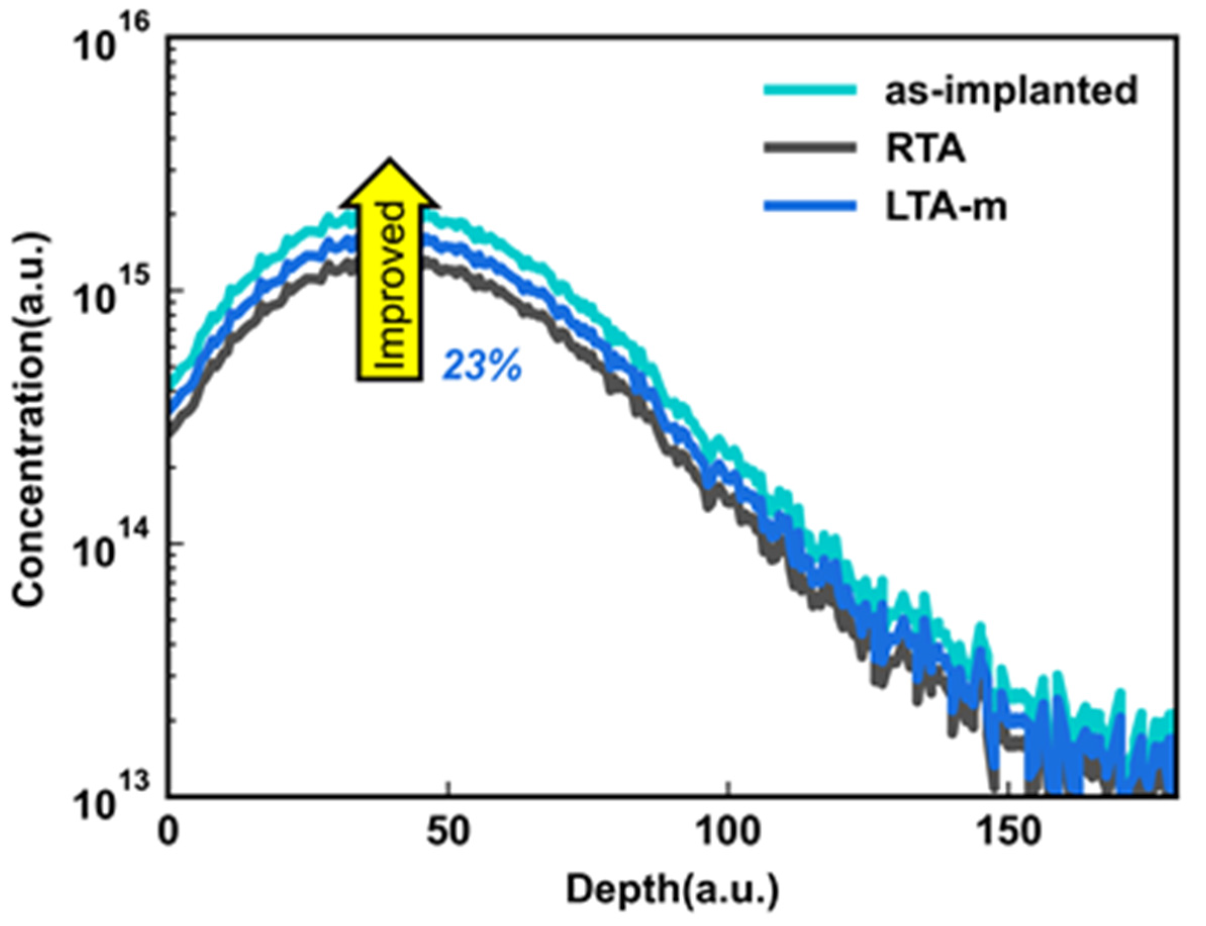
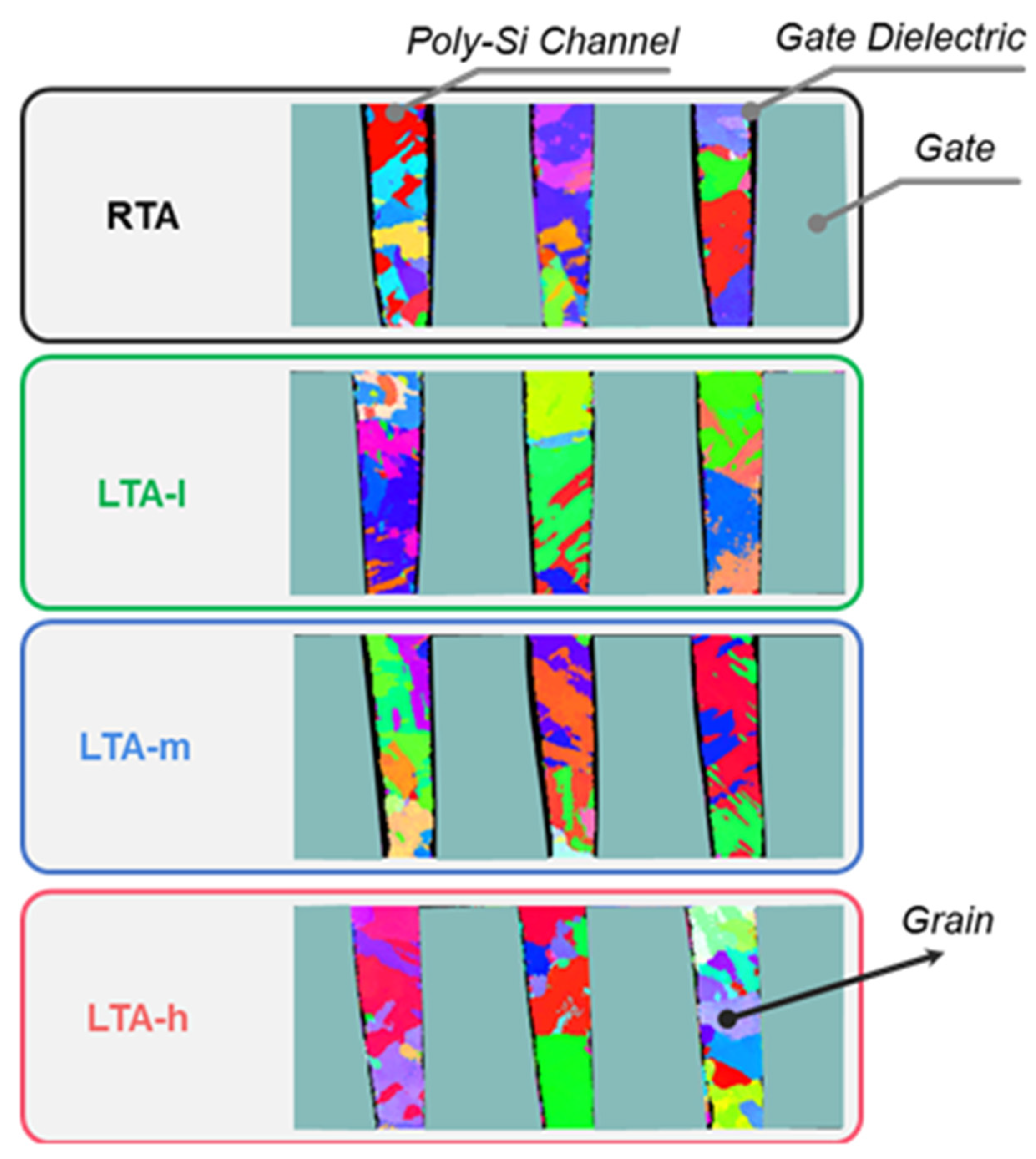
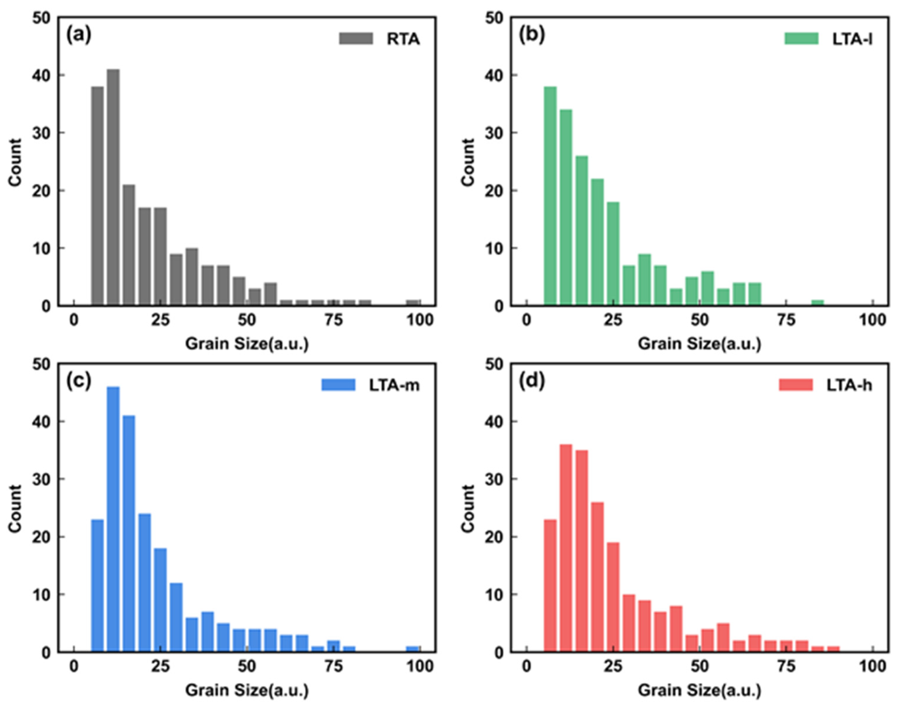
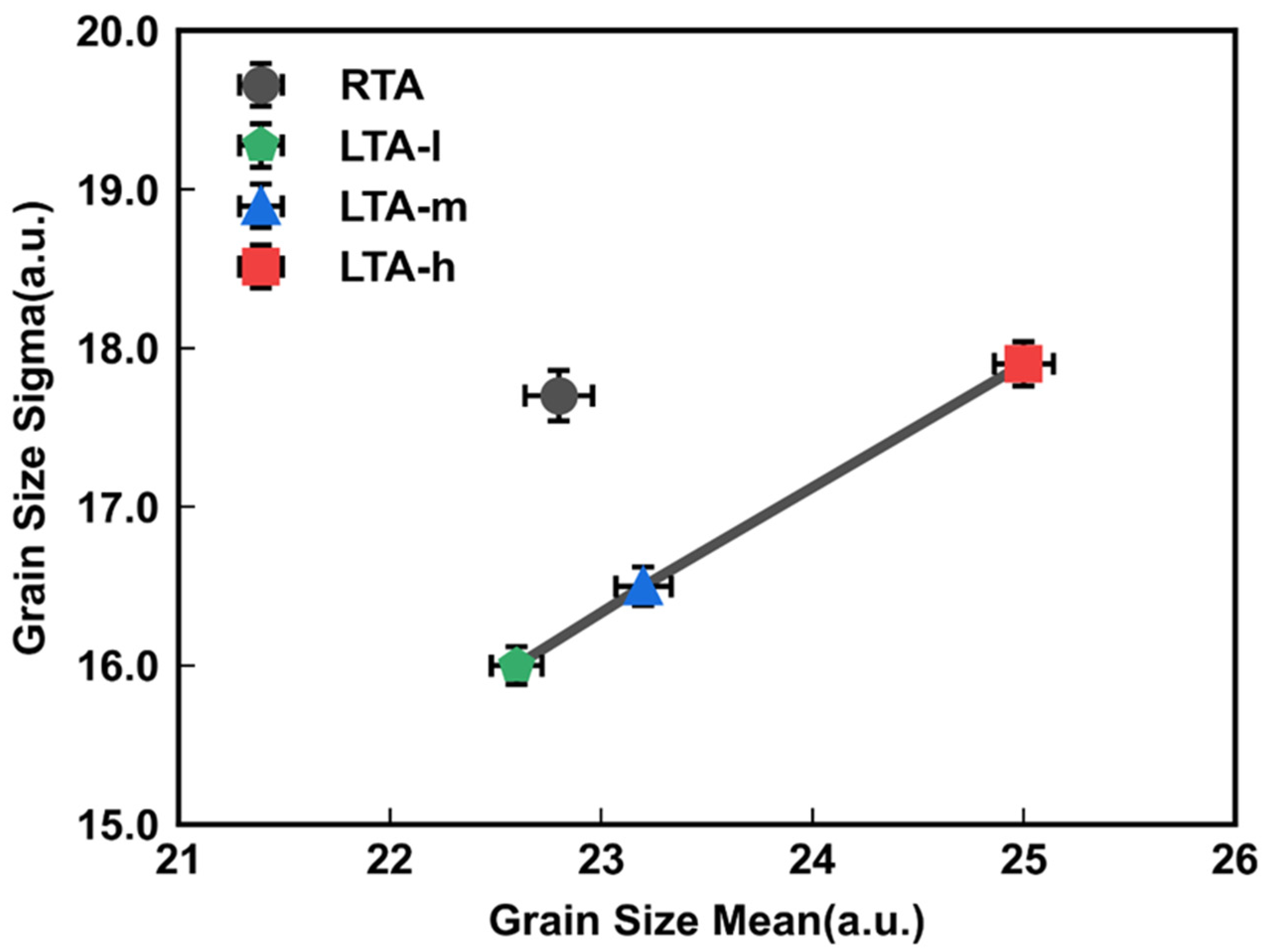
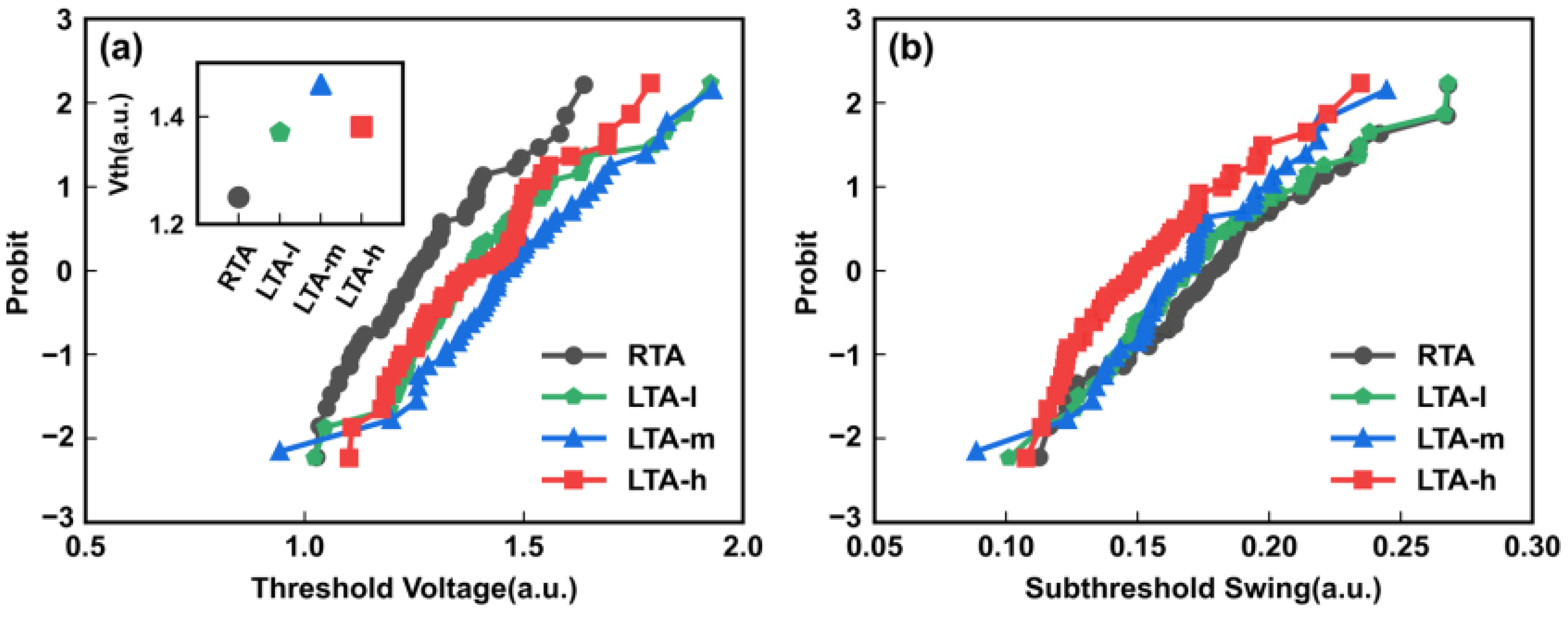
3. Results and Discussion
4. Conclusions
Author Contributions
Funding
Institutional Review Board Statement
Informed Consent Statement
Data Availability Statement
Acknowledgments
Conflicts of Interest
References
- Yamashita, R.; Magia, S.; Higuchi, T.; Yoneya, K.; Yamamura, T.; Mizukoshi, H.; Zaitsu, S.; Yamashita, M.; Toyama, S.; Kamae, N.; et al. A 51 2Gb 3 b/cell flash memory on 64-word-line-layer BiCS technology. In Proceedings of the 2017 IEEE International Solid-State Circuits Conference (ISSCC), San Francisco, CA, USA, 5–9 February 2017; Volume 60, pp. 196–197. [Google Scholar]
- Kim, C.; Cho, J.H.; Jeong, W.; Park, I.H.; Park, H.W.; Kim, D.H.; Kang, D.; Lee, S.; Lee, J.S.; Kim, W.; et al. A 512 Gb 3 b/cell 64-stacked WL 3D V-NAND flash memory. In Proceedings of the 2017 IEEE International Solid-State Circuits Conference (ISSCC), San Francisco, CA, USA, 5–9 February 2017; Volume 60, pp. 202–203. [Google Scholar]
- Lee, S.; Kim, C.; Kim, M.; Joe, S.M.; Jang, J.; Kim, S.; Lee, K.; Kim, J.; Park, J.; Lee, H.J.; et al. A 1 Tb 4 b/cell 64-stacked-WL 3D NAND flash memory with 12 MB/s program throughput. In Proceedings of the 2018 IEEE International Solid—State Circuits Conference—(ISSCC), San Francisco, CA, USA, 11–15 February 2018; Volume 61, pp. 340–342. [Google Scholar]
- Maejima, H.; Kanda, K.; Fujimura, S.; Takagiwa, T.; Ozawa, S.; Sato, J.; Shindo, Y.; Sato, M.; Kanagawa, N.; Musha, J.; et al. A 512 Gb 3 b/Cell 3D flash memory on a 96-word-line-layer technology. In Proceedings of the 2018 IEEE International Solid—State Circuits Conference (ISSCC), San Francisco, CA, USA, 11–15 February 2018; Volume 61, pp. 336–338. [Google Scholar]
- Siau, C.; Kim, K.H.; Lee, S.; Isobe, K.; Shibata, N.; Verma, K.; Ariki, T.; Li, J.; Yuh, J.; Amarnath, A.; et al. A 512 Gb 3-bit/Cell 3D Flash Memory on 128-Wordline-Layer with 132 MB/s Write Performance Featuring Circuit-Under-Array Technology. In Proceedings of the 2019 IEEE International Solid-State Circuits Conference (ISSCC), San Francisco, CA, USA, 17–21 February 2019; pp. 218–220. [Google Scholar]
- Higuchi, T.; Kodama, T.; Kato, K.; Fukuda, R.; Tokiwa, N.; Abe, M.; Takagiwa, T.; Shimizu, Y. A 1 Tb 3 b/Cell 3D-Flash Memory in a 170+ Word-Line-Layer Technology. In Proceedings of the 2021 IEEE International Solid-State Circuits Conference (ISSCC), San Francisco, CA, USA, 13–22 February 2021; pp. 428–430. [Google Scholar]
- Park, J.; Kim, D.; Ok, S.; Park, J.; Kwon, T.; Lee, H.; Lim, S.; Jung, S.; Choi, H.; Kang, T.; et al. A 176-Stacked 512 Gb 3 b/Cell 3D-NAND Flash with 10.8 Gb/mm2 Density with a Peripheral Circuit Under Cell Array Architecture. In Proceedings of the 2021 IEEE International Solid-State Circuits Conference (ISSCC), San Francisco, CA, USA, 13–22 February 2021; pp. 422–423. [Google Scholar]
- Kim, M.; Yun, S.W.; Park, J.; Park, H.K.; Lee, J.; Kim, Y.S.; Na, D.; Choi, S.; Song, Y.; Lee, J.; et al. A 1Tb 3b/Cell 8th-Generation 3D-NAND Flash Memory with 164 MB/s Write Throughput and a 2.4 Gb/s Interface. In Proceedings of the 2022 IEEE International Solid-State Circuits Conference (ISSCC), San Francisco, CA, USA, 20–24 February 2022; pp. 136–137. [Google Scholar]
- Li, Q.; Zhang, Y.; Zou, X.; Gao, J.; Yang, C.; Ding, L.; Wu, Z.; Li, N.; Zhang, S.; Huo, Z. Influence of rapid thermal annealing on the wafer warpage in 3D NAND flash memory. Semicond. Sci. Technol. 2019, 34, 02LT01. [Google Scholar] [CrossRef]
- Shi, D.; Xia, Z.; Hu, M.; Mei, G.; Huo, Z. A novel solution to improve saddle-shape warpage in 3D NAND flash memory. Semicond. Sci. Technol. 2020, 35, 045031. [Google Scholar] [CrossRef]
- Huo, Z.; Cheng, W.; Yang, S. Unleash Scaling Potential of 3D NAND with Innovative Xtacking® Architecture. In Proceedings of the 2022 IEEE Symposium on VLSI Technology and Circuits (VLSI Technology and Circuits), Honolulu, HI, USA, 12–17 June 2022; pp. 254–255. [Google Scholar]
- Song, Y.; Xia, Z.; Hua, W.; Liu, F.; Huo, Z. Modeling and optimization of Array Leakage in 3D NAND Flash Memory. In Proceedings of the 2018 IEEE International Conference on Integrated Circuits, Technologies and Applications (ICTA), Beijing, China, 21–23 November 2018; pp. 120–121. [Google Scholar]
- Gutt, T.; Schulze, H. Deep melt activation using laser thermal annealing for IGBT thin wafer technology. In Proceedings of the 2010 22nd International Symposium on Power Semiconductor Devices & IC’s (ISPSD), Hiroshima, Japan, 6–10 June 2010; pp. 29–32. [Google Scholar]
- Venturini, J. Laser Thermal Annealing: Enabling ultra-low thermal budget processes for 3D junctions formation and devices. In Proceedings of the 2012 12th International Workshop on Junction Technology, Shanghai, China, 14–15 May 2012; pp. 57–62. [Google Scholar]
- Huet, K.; Toqué-Tresonne, I.; Mazzamuto, F.; Emeraud, T.; Besaucèle, H. Laser thermal annealing: A low thermal budget solution for advanced structures and new materials. In Proceedings of the 2014 International Workshop on Junction Technology (IWJT), Shanghai, China, 18–20 May 2014; pp. 1–6. [Google Scholar]
- Rosseel, E.; Dhayalan, S.K.; Hikavyy, A.Y.; Loo, R.; Profijt, H.B.; Kohen, D.; Kubicek, S.; Chiarella, T.; Yu, H.; Horiguchi, N.; et al. Selective epitaxial growth of high-P Si: P for source/drain formation in advanced Si nFETs. ECS Trans. 2016, 75, 347. [Google Scholar] [CrossRef]
- Hung, R.; Khaja, F.A.; Hollar, K.E.; Rao, K.V.; Munnangi, S.; Chen, Y.; Okazaki, M.; Huang, Y.-C.; Li, X.; Chung, H.; et al. Novel solutions to enable contact resistivity<1E-9 Ω-cm2 for 5 nm node and beyond. In Proceedings of the 2018 International Symposium on VLSI Technology, Systems and Application (VLSI-TSA), Hsinchu, Taiwan, 16–19 April 2018; pp. 1–2. [Google Scholar]
- Fenouillet-Beranger, C.; Brunet, L.; Batude, P.; Brevard, L.; Garros, X.; Cassé, M.; Lacord, J.; Sklenard, B.; Acosta-Alba, P.; Kerdilès, S.; et al. A review of low temperature process modules leading up to the first (≤500 °C) planar FDSOI CMOS devices for 3-D sequential integration. IEEE Trans. Electron Devices 2021, 68, 3142–3148. [Google Scholar] [CrossRef]
- Huet, K.; Tabata, T.; Aubin, J.; Rozé, F.; Thuries, L.; Halty, S.; Curvers, B.; Mazzamuto, F.; Liu, J.; Mori, Y. Laser thermal annealing for low thermal budget applications: From contact formation to material modification. ECS Trans. 2019, 89, 137. [Google Scholar] [CrossRef]
- Lisoni, J.G.; Arreghini, A.; Congedo, G.; Toledano-Luque, M.; Toqué-Tresonne, I.; Huet, K.; Capogreco, E.; Liu, L.; Tan, C.-L.; Degraeve, R.; et al. Laser Thermal Anneal of polysilicon channel to boost 3D memory performance. In Proceedings of the 2014 Symposium on VLSI Technology (VLSI-Technology): Digest of Technical Papers, Honolulu, HI, USA, 9–12 June 2014; pp. 1–2. [Google Scholar]
- Son, Y.-I.; Shin, J. Numerical Study on the Laser Annealing of Silicon Used in Advanced V-NAND Device. Materials 2022, 15, 4201. [Google Scholar] [CrossRef] [PubMed]
- Yang, T.; Xia, Z.; Shi, D.; Ouyang, Y.; Huo, Z. Analysis and optimization of threshold voltage variability by polysilicon grain size simulation in 3D NAND flash memory. IEEE J. Electron. Devices Soc. 2020, 8, 140–144. [Google Scholar] [CrossRef]
Disclaimer/Publisher’s Note: The statements, opinions and data contained in all publications are solely those of the individual author(s) and contributor(s) and not of MDPI and/or the editor(s). MDPI and/or the editor(s) disclaim responsibility for any injury to people or property resulting from any ideas, methods, instructions or products referred to in the content. |
© 2023 by the authors. Licensee MDPI, Basel, Switzerland. This article is an open access article distributed under the terms and conditions of the Creative Commons Attribution (CC BY) license (https://creativecommons.org/licenses/by/4.0/).
Share and Cite
Yang, T.; Xia, Z.; Fan, D.; Zhao, D.; Xie, W.; Yang, Y.; Liu, L.; Zhou, W.; Huo, Z. Activation Enhancement and Grain Size Improvement for Poly-Si Channel Vertical Transistor by Laser Thermal Annealing in 3D NAND Flash. Micromachines 2023, 14, 230. https://doi.org/10.3390/mi14010230
Yang T, Xia Z, Fan D, Zhao D, Xie W, Yang Y, Liu L, Zhou W, Huo Z. Activation Enhancement and Grain Size Improvement for Poly-Si Channel Vertical Transistor by Laser Thermal Annealing in 3D NAND Flash. Micromachines. 2023; 14(1):230. https://doi.org/10.3390/mi14010230
Chicago/Turabian StyleYang, Tao, Zhiliang Xia, Dongyu Fan, Dongxue Zhao, Wei Xie, Yuancheng Yang, Lei Liu, Wenxi Zhou, and Zongliang Huo. 2023. "Activation Enhancement and Grain Size Improvement for Poly-Si Channel Vertical Transistor by Laser Thermal Annealing in 3D NAND Flash" Micromachines 14, no. 1: 230. https://doi.org/10.3390/mi14010230
APA StyleYang, T., Xia, Z., Fan, D., Zhao, D., Xie, W., Yang, Y., Liu, L., Zhou, W., & Huo, Z. (2023). Activation Enhancement and Grain Size Improvement for Poly-Si Channel Vertical Transistor by Laser Thermal Annealing in 3D NAND Flash. Micromachines, 14(1), 230. https://doi.org/10.3390/mi14010230