
Development of MEMS Process Compatible (Bi,Sb)2(Se,Te)3-Based Thin Films for Scalable Fabrication of Planar Micro-Thermoelectric Generators


Abstract
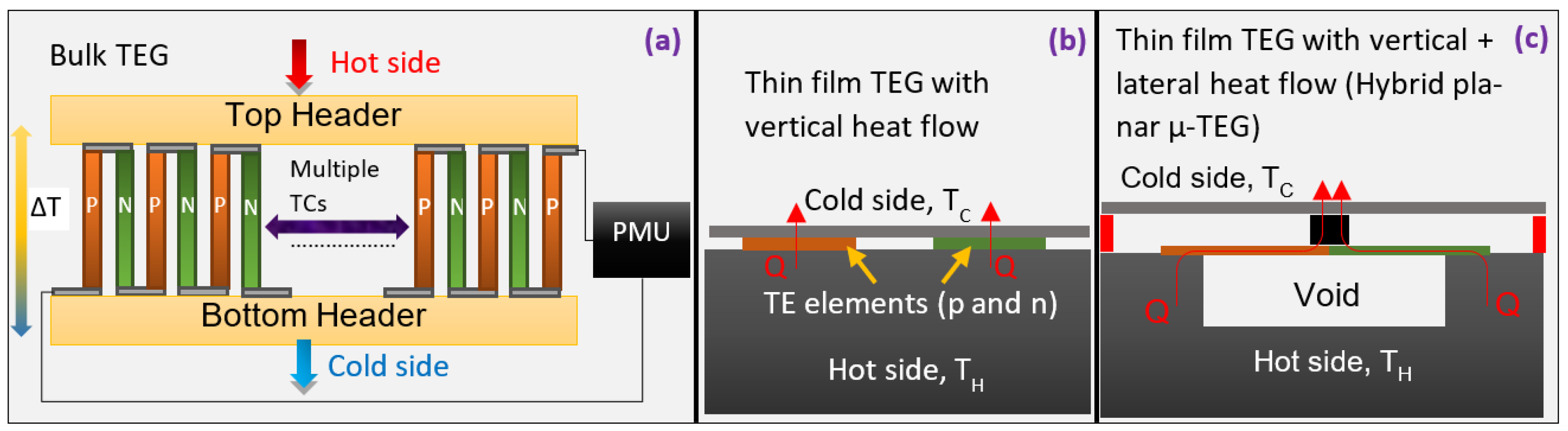
:1. Introduction
2. Experimental
3. Results and Discussion
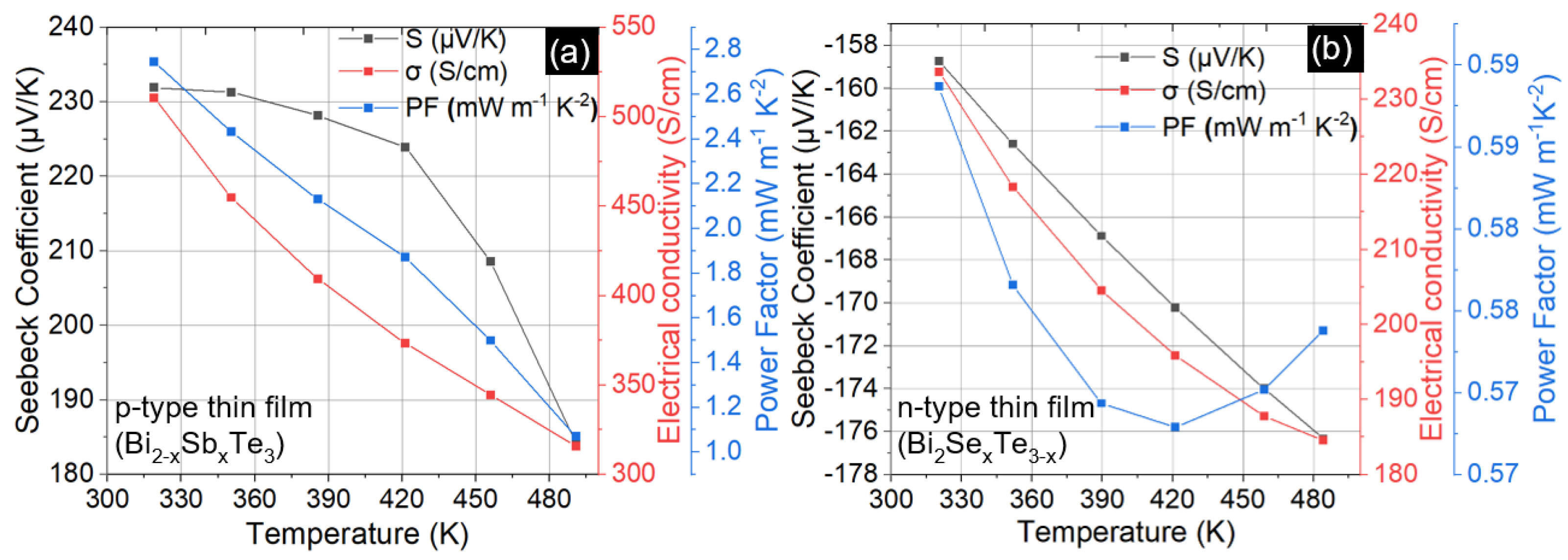
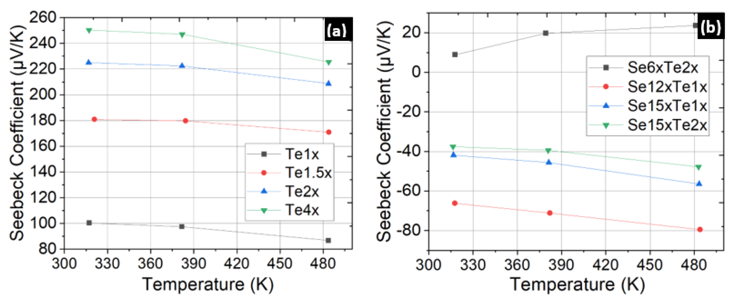
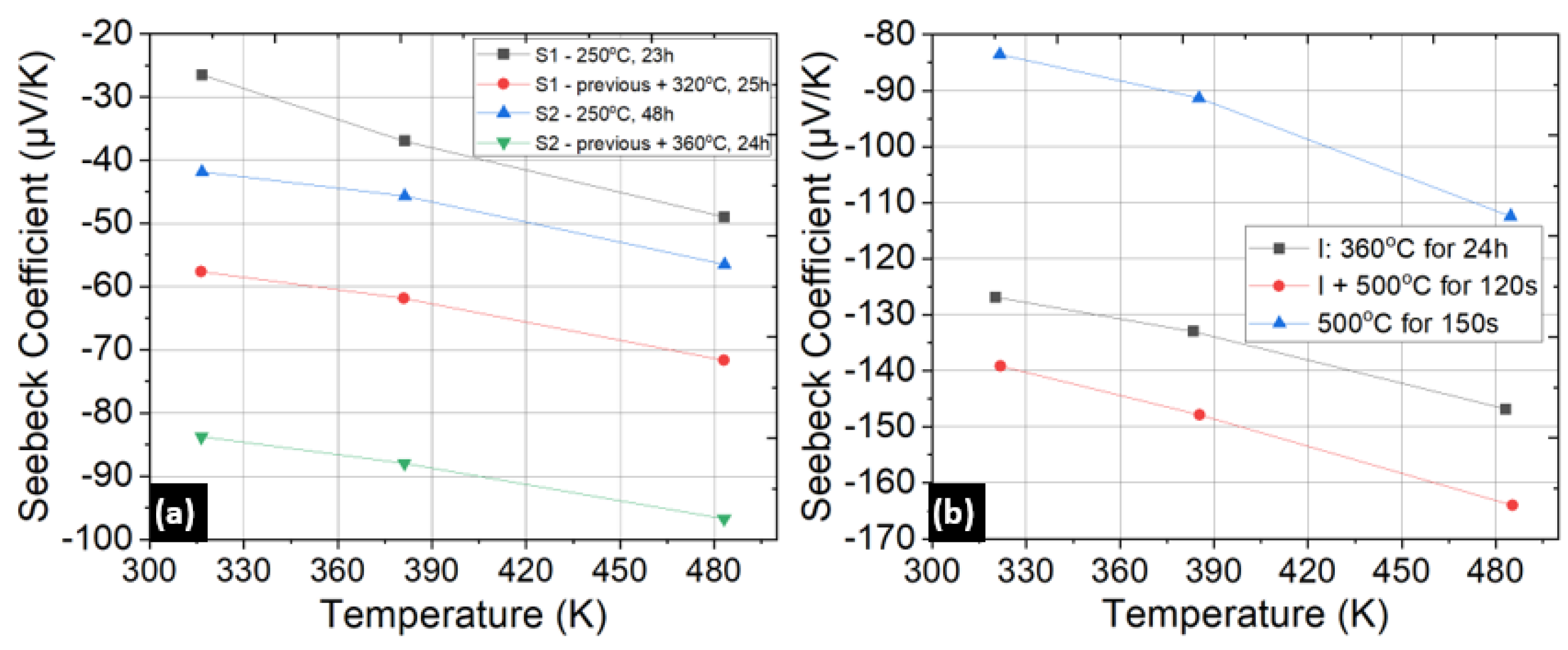
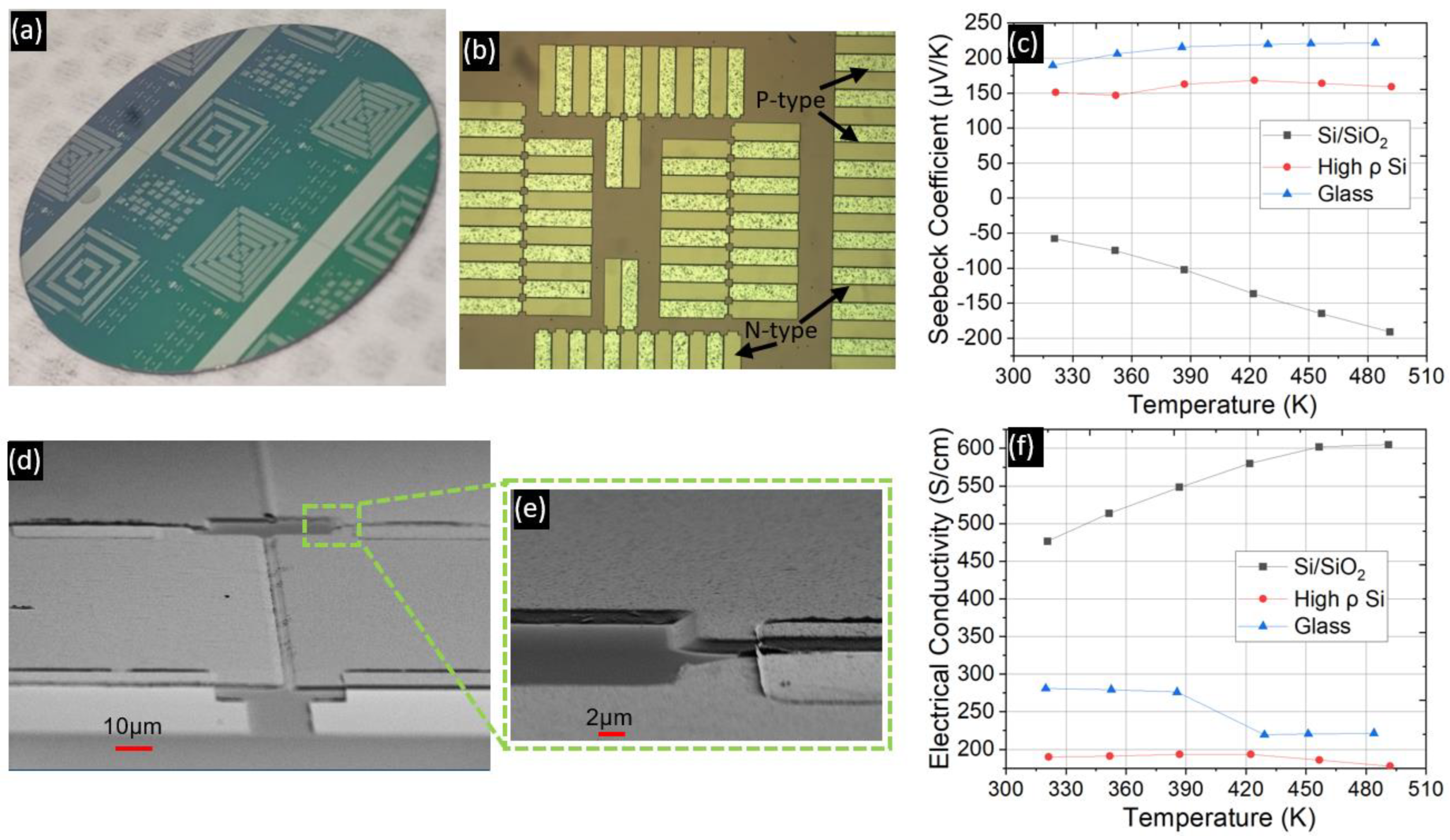
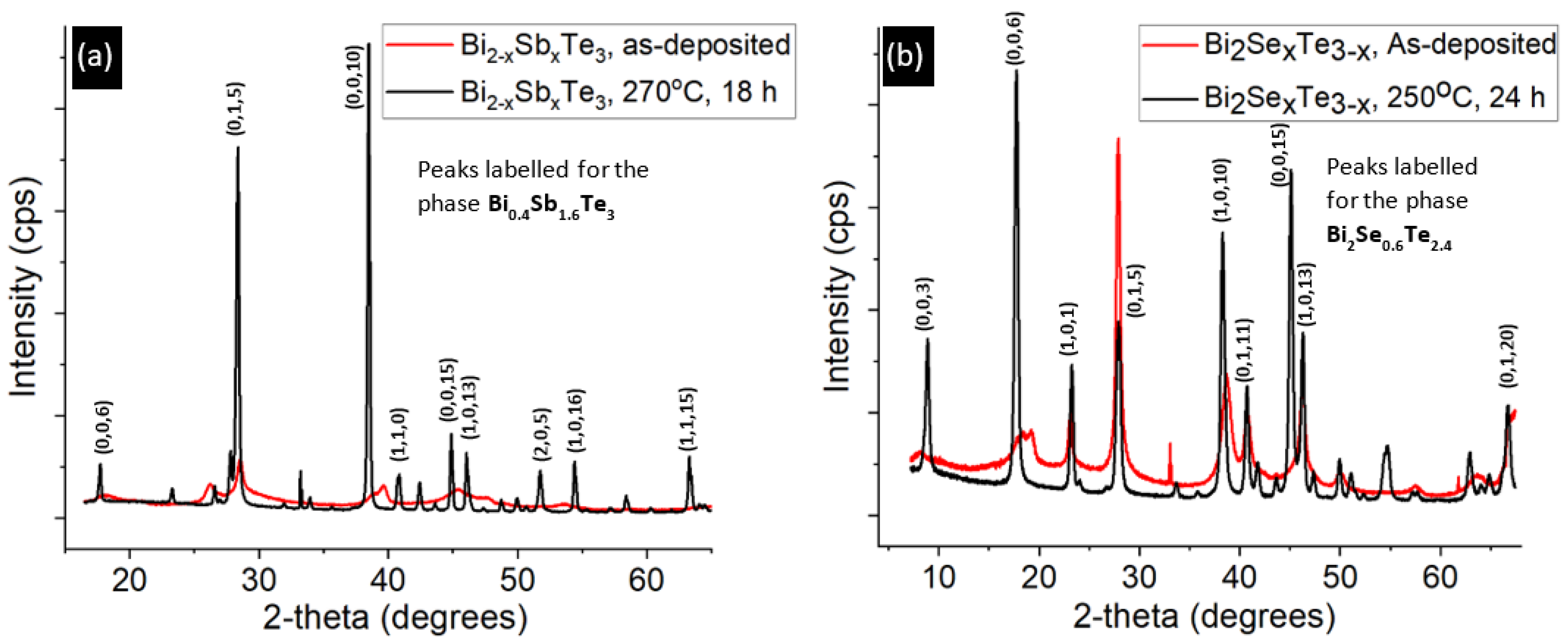
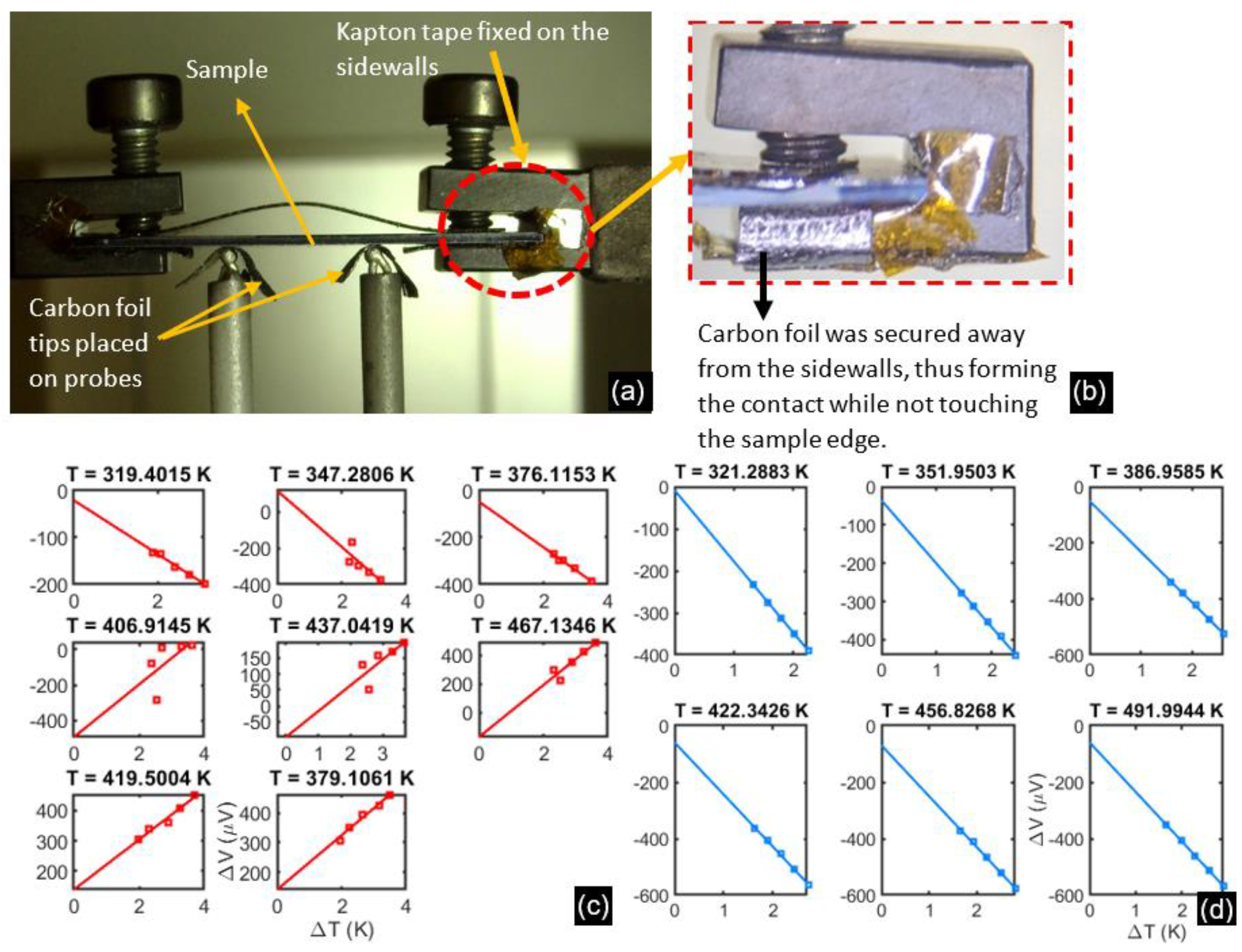
3.1. Optimization of Thin Film Thermoelectric Properties
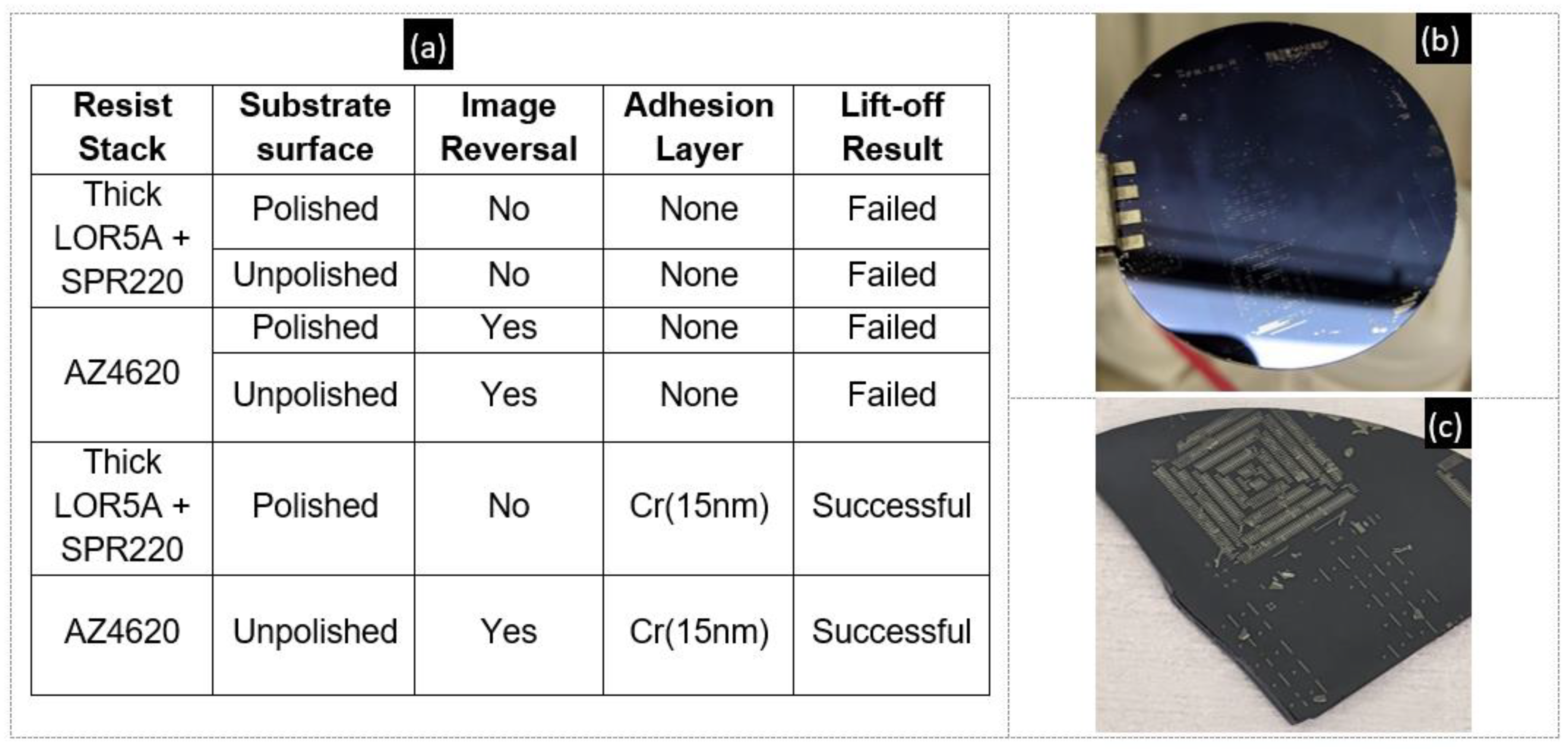
3.2. Lift-Off of Thermoelectric Thin Films
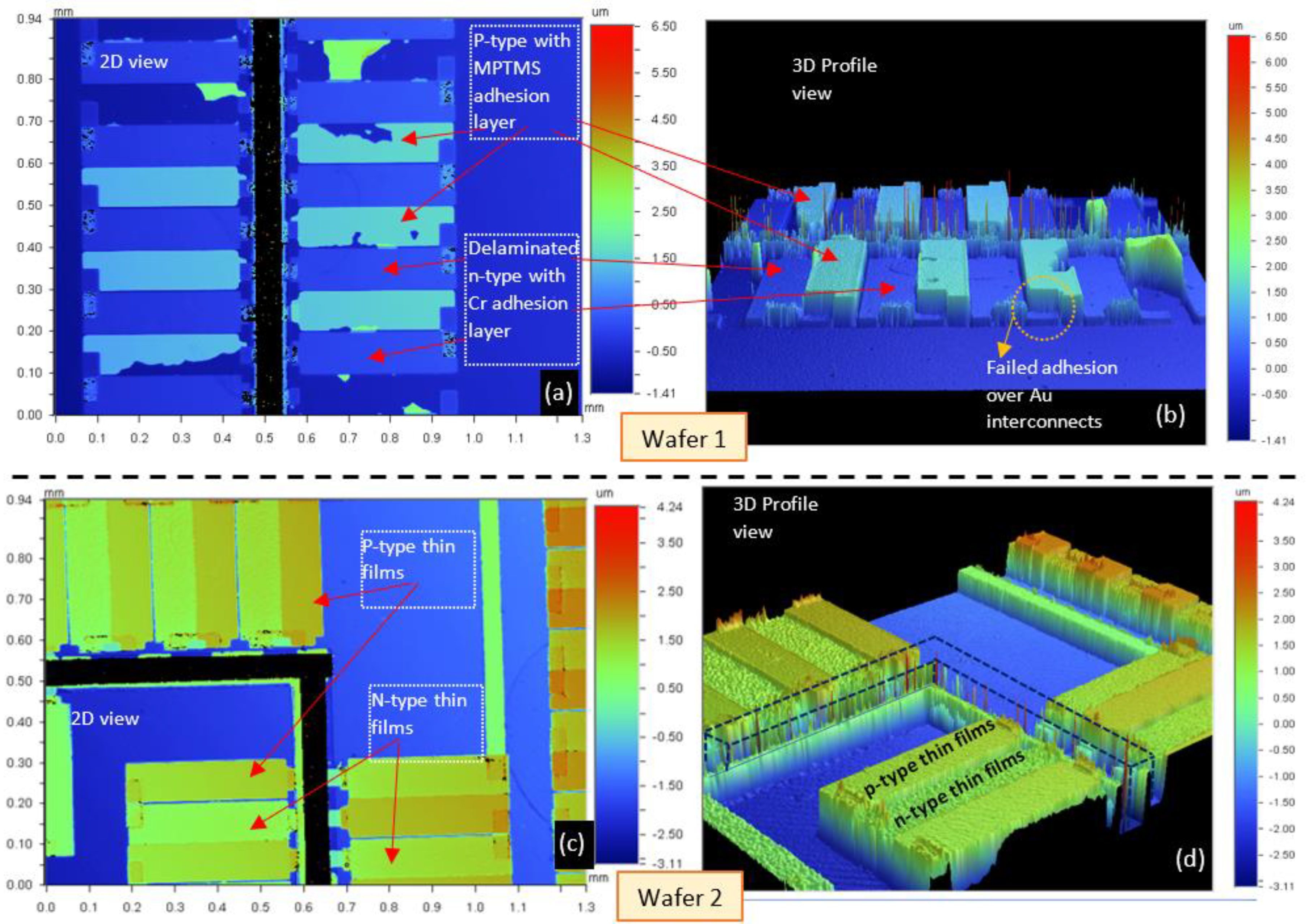
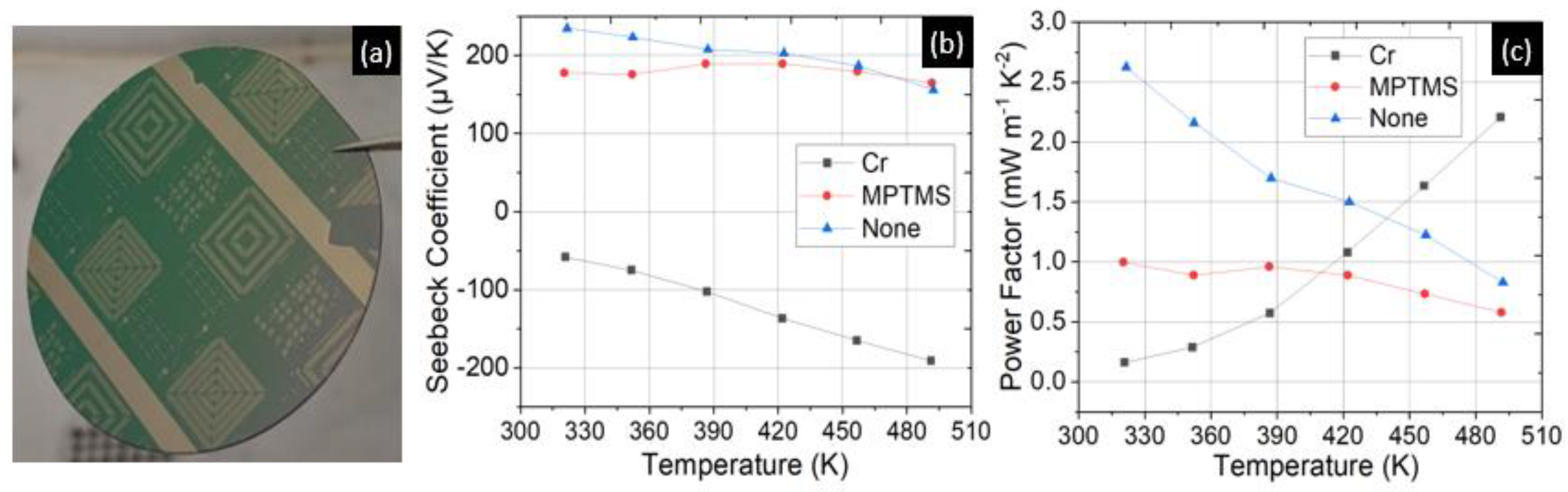
3.3. Alternative Adhesion Layer
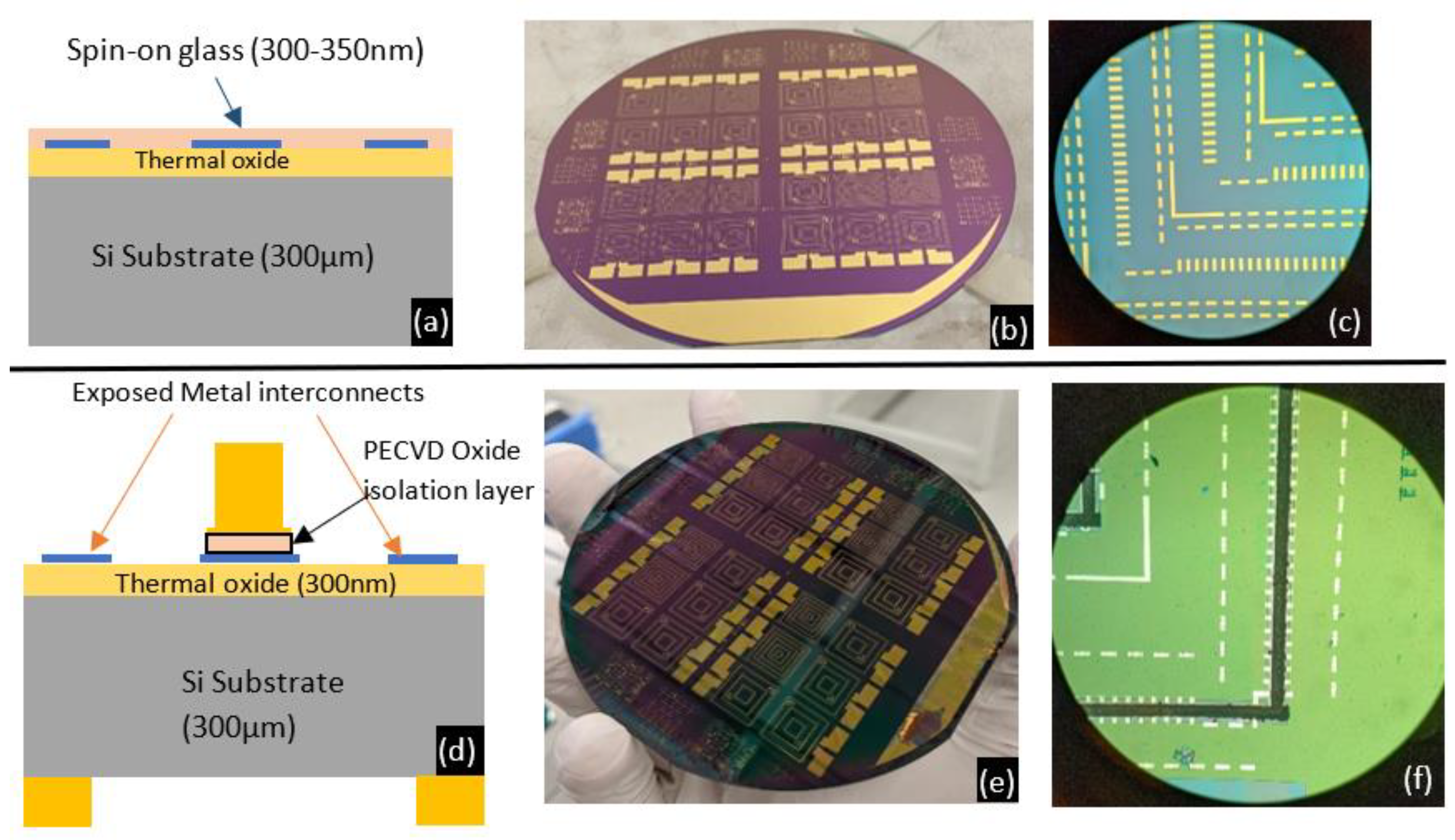
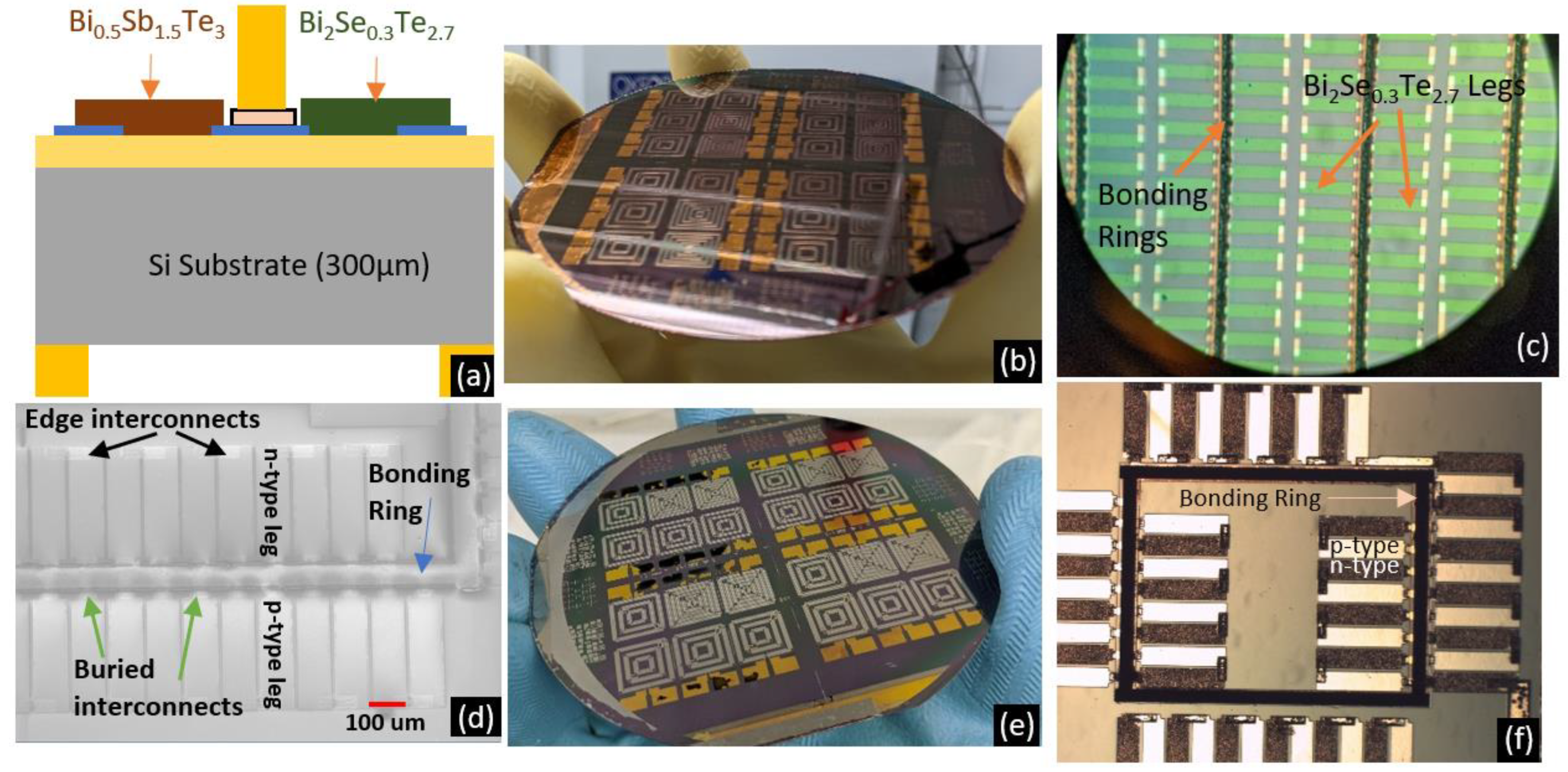
3.4. Results from Pre-Packaging Fabrication Steps
4. Conclusions
Author Contributions
Funding
Institutional Review Board Statement
Informed Consent Statement
Data Availability Statement
Conflicts of Interest
References
- Mukhopadhyay, S.C.; Suryadevara, N.K. Internet of Things: Challenges and Opportunities. In Internet of Things. Smart Sensors, Measurement and Instrumentation; Mukhopadhyay, S., Ed.; Springer: Cham, Switzerland, 2014; Volume 9. [Google Scholar] [CrossRef]
- Avatefipour, O.; Sadry, F. Traffic Management System Using IoT Technology—A Comparative Review. In Proceedings of the 2018 IEEE International Conference on Electro/Information Technology (EIT), Rochester, MI, USA, 3–5 May 2018; pp. 1041–1047. [Google Scholar] [CrossRef]
- Raposo, D.; Rodrigues, A.; Sinche, S.; Sá Silva, J.; Boavida, F. Industrial IoT Monitoring: Technologies and Architecture Proposal. Sensors 2018, 18, 3568. [Google Scholar] [CrossRef] [PubMed]
- Gaikwad, P.P.; Gabhane, J.P.; Golait, S.S. A survey based on Smart Homes system using Internet-of-Things. In Proceedings of the 2015 International Conference on Computation of Power, Energy, Information and Communication (ICCPEIC), Chennai, India, 22–23 April 2015; pp. 330–335. [Google Scholar] [CrossRef]
- Lou, Z.; Wang, L.; Jiang, K.; Wei, Z.; Shen, G. Reviews of wearable healthcare systems: Materials, devices and system integration. Mater. Sci. Eng. R Rep. 2020, 140, 100523. [Google Scholar] [CrossRef]
- Nozariasbmarz, A.; Krasinski, J.S.; Vashaee, D. N-Type Bismuth Telluride Nanocomposite Materials Optimization for Thermoelectric Generators in Wearable Applications. Materials 2019, 12, 1529. [Google Scholar] [CrossRef]
- Everactive. Everactive’s Evernet Protocol, Unlocking the Internet of Things at Scale. Available online: https://everactive.com/whitepapers/everactives-evernet-protocol-unlocking-the-internet-of-things-at-scale/ (accessed on 17 July 2022).
- Raj, A.; Steingart, D. Review—Power Sources for the Internet of Things. J. Electrochem. Soc. 2018, 165, B3130–B3136. [Google Scholar] [CrossRef]
- Hasan, N.; Sahlan, S.; Osman, K.; Ali, M.S.M. Energy Harvesters for Wearable Electronics and Biomedical Devices. Adv. Mater. Technol. 2021, 6, 2000771. [Google Scholar] [CrossRef]
- Jaziri, N.; Boughamoura, A.; Müller, J.; Mezghani, B.; Tounsi, F.; Ismail, M. A comprehensive review of Thermoelectric Generators: Technologies and common applications. Energy Rep. 2020, 6, 264–287. [Google Scholar] [CrossRef]
- Nozariasbmarz, A.; Collins, H.; Dsouza, K.; Polash, M.H.; Hosseini, M.; Hyland, M.; Liu, J.; Malhotra, A.; Ortiz, F.M.; Mohaddes, F.; et al. Review of wearable thermoelectric energy harvesting: From body temperature to electronic systems. Appl. Energy 2020, 258, 114069. [Google Scholar] [CrossRef]
- Zhou, M.; Al-Furjan, M.S.H.; Zou, J.; Liu, W. A review on heat and mechanical energy harvesting from human--Principles, prototypes and perspectives. Renew. Sustain. Energy Rev. 2018, 82, 3582–3609. [Google Scholar] [CrossRef]
- Wu, C.; Wang, A.; Ding, W.; Guo, H.; Wang, Z.L. Triboelectric Nanogenerator: A Foundation of the Energy for the New Era. Adv. Energy Mater. 2019, 9, 1802906. [Google Scholar] [CrossRef]
- Hashemi, S.A.; Ramakrishna, S.; Aberle, A.G. Recent progress in flexible–wearable solar cells for self-powered electronic devices. Energy Environ. Sci. 2020, 13, 685–743. [Google Scholar] [CrossRef]
- Nozariasbmarz, A.; Suarez, F.; Dycus, J.H.; Cabral, M.J.; LeBeau, J.M.; Öztürk, M.C.; Vashaee, D. Thermoelectric generators for wearable body heat harvesting: Material and device concurrent optimization. Nano Energy 2020, 67, 104265. [Google Scholar] [CrossRef]
- Poudel, B.; Hao, Q.; Ma, Y.; Lan, Y.; Minnich, A.; Yu, B.; Yan, X.; Wang, D.; Muto, A.; Vashaee, D.; et al. High-Thermoelectric Performance of Nanostructured Bismuth Antimony Telluride Bulk Alloys. Science 2008, 320, 634–638. [Google Scholar] [CrossRef] [PubMed]
- Hu, L.; Wu, H.; Zhu, T.; Fu, C.; He, J.; Ying, P.; Zhao, X. Tuning Multiscale Microstructures to Enhance Thermoelectric Performance of n-Type Bismuth-Telluride-Based Solid Solutions. Adv. Energy Mater. 2015, 5, 1500411. [Google Scholar] [CrossRef]
- Yan, J.; Liao, X.; Yan, D.; Chen, Y. Review of Micro Thermoelectric Generator. J. Microelectromech. Syst. 2018, 27, 1–18. [Google Scholar] [CrossRef]
- Yang, S.M.; Wang, J.Y.; Chen, M.D.; Tsai, M.H. Development of a Thermoelectric Energy Generator Chip of Small Layout and High Power/Voltage Factors by Foundry Service. IEEE Sens. J. 2019, 19, 9149–9155. [Google Scholar] [CrossRef]
- Ziouche, K.; Yuan, Z.; Lejeune, P.; Lasri, T.; Leclercq, D.; Bougrioua, Z. Silicon-Based Monolithic Planar Micro Thermoelectric Generator Using Bonding Technology. J. Microelectromech. Syst. 2017, 26, 45–47. [Google Scholar] [CrossRef]
- Da Silva L, Kaviany M, Fabrication and Measured performance of a First-Generation Microthermoelectric Cooler. J. Microelectromech. Syst. 2005, 14, 1110–1117. [CrossRef]
- Tang, X.; Li, Z.; Liu, W.; Zhang, Q.; Uher, C. A comprehensive review on Bi2Te3-based thin films: Thermoelectrics and beyond. Interdiscip. Mater. 2022, 1, 88–115. [Google Scholar] [CrossRef]
- Da Silva, L.W.; Kaviany, M.; Uher, C. Thermoelectric performance of films in the bismuth-tellurium and antimony-tellurium systems. J. Appl. Phys. 2005, 97, 114903. [Google Scholar] [CrossRef]
- Goncalves, L.; Couto, C.; Alpuim, P.; Rolo, A.; Völklein, F.; Correia, J. Optimization of thermoelectric properties on Bi2Te3 thin films deposited by thermal co-evaporation. Thin Solid Films 2010, 518, 2816–2821. [Google Scholar] [CrossRef]
- Deng, Y.; Liang, H.-M.; Wang, Y.; Zhang, Z.-W.; Tan, M.; Cui, J.-L. Growth and transport properties of oriented bismuth telluride films. J. Alloys Compd. 2011, 509, 5683–5687. [Google Scholar] [CrossRef]
- Kim, H.-J.; Yim, J.; Choi, W.C.; Park, C.; Kim, J. The Effect of annealing in controlled vapor pressure on the thermoelectric properties of RF-sputtered Bi2Te3 film. J. Electron. Mater. 2012, 41, 1519–1523. [Google Scholar] [CrossRef]
- Aabdin, Z.; Peranio, N.; Winkler, M.; Bessas, D.; König, J.; Hermann, R.P.; Böttner, H.; Eibl, O. Sb2Te3 and Bi2Te3 Thin films grown by room-temperature MBE. J. Electron. Mater. 2012, 41, 1493–1497. [Google Scholar] [CrossRef]
- Winkler, M.; Liu, X.; König, J.D.; Buller, S.; Schürmann, U.; Kienle, L.; Bensch, W.; Böttner, H. Electrical and structural properties of Bi2Te3 and Sb2Te3 thin films grown by the nanoalloying method with different deposition patterns and compositions. J. Mater. Chem. 2012, 22, 11323–11334. [Google Scholar] [CrossRef]
- Li Bassi, A.; Bailini, A.; Casari, C.S.; Donati, F.; Mantegazza, A.; Passoni, M.; Russo, V.; Bottani, C.E. Thermoelectric properties of Bi–Te films with controlled structure and morphology. J. Appl. Phys. 2009, 105, 124307. [Google Scholar] [CrossRef]
- Symeou, E.; Pervolaraki, M.; Mihailescu, C.; Athanasopoulos, G.; Papageorgiou, C.; Kyratsi, T.; Giapintzakis, J. Thermoelectric properties of Bi0.5Sb1.5Te3 thin films grown by pulsed laser deposition. Appl. Surf. Sci. 2015, 336, 138–142. [Google Scholar] [CrossRef]
- Takashiri, M.; Shirakawa, T.; Miyazaki, K.; Tsukamoto, H. Fabrication and characterization of bismuth–telluride-based 110 | TANG ET AL. alloy thin film thermoelectric generators by flash evaporation method. Sens. Actuators A Phys. 2007, 138, 329–334. [Google Scholar] [CrossRef] [Green Version]
- Parashchuk, T.; Kostyuk, O.; Nykyruy, L.; Dashevsky, Z. High thermoelectric performance of p-type Bi0.5Sb1.5Te3 films on flexible substrate. Mater. Chem. Phys. 2020, 253, 123427. [Google Scholar] [CrossRef]
- Huang, B.; Lawrence, C.; Gross, A.; Hwang, G.-S.; Ghafouri, N.; Lee, S.-W.; Kim, H.; Li, C.-P.; Uher, C.; Najafi, K.; et al. Low-temperature characterization and micropatterning of coevaporated Bi2Te3 and Sb2Te3 films. J. Appl. Phys. 2008, 104, 113710. [Google Scholar] [CrossRef]
- Bourgault, D.; Garampon, C.G.; Caillault, N.; Carbone, L.; Aymami, J. Thermoelectric properties of n-type Bi2Te2.7Se0.3 and p-type Bi0.5Sb1.5Te3 thin films deposited by direct current magnetron sputtering. Thin. Solid Films 2008, 516, 8579–8583. [Google Scholar] [CrossRef]
- Ao, D.; Liu, W.; Chen, Y.; Wei, M.; Jabar, B.; Li, F.; Shi, X.; Zheng, Z.; Liang, G.; Zhang, X.; et al. Novel Thermal Diffusion Temperature Engineering Leading to High Thermoelectric Performance in Bi2Te3-Based Flexible Thin-Films. Adv. Sci. 2022, 9, 2103547. [Google Scholar] [CrossRef] [PubMed]
- Shea, R.; Gawarikar, A.; Talghader, J. Process Integration of Co-Sputtered Bismuth Telluride/Antimony Telluride Thermoelectric Junctions. J. Microelectromech. Syst. 2014, 23, 681–688. [Google Scholar] [CrossRef]
- Satyala, N.; Rad, A.T.; Zamanipour, Z.; Norouzzadeh, P.; Krasinski, J.S.; Tayebi, L.; Vashaee, D. Reduction of thermal conductivity of bulk nanostructured bismuth telluride composites embedded with silicon nano-inclusions. J. Appl. Phys. 2014, 115, 44304. [Google Scholar] [CrossRef]
- Dresselhaus, M.; Chen, G.; Ren, Z.; Fleurial, J.-P.; Gogna, P.; Tang, M.Y.; Vashaee, D.; Lee, H.; Wang, X.; Joshi, G.; et al. Nanocomposites to Enhance ZT in Thermoelectrics, MRS Online Proceedings Library (OPL); Cambridge University Press: Cambridge, UK, 2007; Volume 1044. [Google Scholar] [CrossRef]
- Vashaee, D.; Zhang, Y.; Shakouri, A.; Zeng, G.; Chiu, Y.-J. Cross-plane Seebeck coefficient in superlattice structures in the miniband conduction regime. Phys. Rev. B 2006, 74, 195315. [Google Scholar] [CrossRef]
- Tayebi, L.; Zamanipour, Z.; Vashaee, D. Design optimization of micro-fabricated thermoelectric devices for solar power generation. Renew. Energy 2014, 69, 166–173. [Google Scholar] [CrossRef]
- Gonçalves, L.; Alpuim, P.; Rolo, A.; Correia, J. Thermal co-evaporation of Sb2Te3 thin-films optimized for thermoelectric applications. Thin Solid Films 2011, 519, 4152–4157. [Google Scholar] [CrossRef]
- Matweb—The Online materials Information Resource. Available online: https://www.matweb.com/ (accessed on 10 July 2022).
- Ghafouri, N. Bismuth Telluride and Antimony Telluride Based Co-Evaporated Thermoelectric Thin Films: Technology, Characterization and Optimization; University of Michigan: Ann Arbor, MI, USA, 2012. [Google Scholar]
- Sasaki, Y.; Takashiri, M. Effects of Cr interlayer thickness on adhesive, structural, and thermoelectric properties of antimony telluride thin films deposited by radio-frequency magnetron sputtering. Thin Solid Films 2016, 619, 195–201. [Google Scholar] [CrossRef]
- Yüzüak, G.; Çiçek, M.; Elerman, Y.; Yüzüak, E. Enhancing the power factor of p-type BiSbTe films via deposited with/without Cr seed layer. J. Alloys Compd. 2021, 886, 161263. [Google Scholar] [CrossRef]
- Mizoshiri, M.; Mikami, M.; Ozaki, K. The effect of Cr buffer layer thickness on voltage generation of thin-film thermoelectric modules. J. Micromech. Microeng. 2013, 23, 115016. [Google Scholar] [CrossRef]
- Colas, F.; Barchiesi, D.; Kessentini, S.; Toury, T.; De La Chapelle, M.L. Comparison of adhesion layers of gold on silicate glasses for SERS detection. J. Opt. 2015, 17, 114010. [Google Scholar] [CrossRef]
- Mahapatro, A.K.; Scott, A.; Manning, A.; Janes, D.B. Gold surface with sub-nm roughness realized by evaporation on a molecular adhesion monolayer. Appl. Phys. Lett. 2006, 88, 151917. [Google Scholar] [CrossRef]
- Gothe, P.K.; Gaur, D.; Achanta, V.G. MPTMS self-assembled monolayer deposition for ultra-thin gold films for plasmonics. J. Phys. Commun. 2018, 2, 035005. [Google Scholar] [CrossRef]
- Liufu, S.-C.; Chen, L.-D.; Yao, Q.; Wang, C.-F. Assembly of one-dimensional nanorods into Bi2S3 films with enhanced thermoelectric transport properties. Appl. Phys. Lett. 2007, 90, 112106. [Google Scholar] [CrossRef]
- Cardinal, T.; Kwan, M.; Borca-Tasciuc, T.; Ramanath, G. Multifold Electrical Conductance Enhancements at Metal–Bismuth Telluride Interfaces Modified Using an Organosilane Monolayer. ACS Appl. Mater. Interfaces 2017, 9, 2001–2005. [Google Scholar] [CrossRef] [PubMed]
- Morikawa, S.; Satake, Y.; Takashiri, M. Characteristics of nanostructured bismuth telluride thin films fabricated by oblique deposition. Vacuum 2018, 148, 296–302. [Google Scholar] [CrossRef]
- Yonezawa, S.; Tabuchi, T.; Takashiri, M. Atomic composition changes in bismuth telluride thin films by thermal annealing and estimation of their thermoelectric properties using experimental analyses and first-principles calculations. J. Alloys Compd. 2020, 841, 155697. [Google Scholar] [CrossRef]
- Haidar, S.A.; Gao, Y.; He, Y.; Cornett, J.E.; Chen, B.; Coburn, N.J.; Glynn, C.; Dunham, M.T.; Goodson, K.E.; Sun, N. Deposition and Fabrication of Sputtered Bismuth Telluride and Antimony Telluride for Microscale Thermoelectric Energy Harvesters. Thin Solid Films 2021, 717, 138444. [Google Scholar] [CrossRef]
- Naumochkin, M.; Park, G.-H.; Nielsch, K.; Reith, H. Study of the Annealing Effects of Sputtered Bi2Te3 Thin Films with Full Thermoelectric Figure of Merit Characterization. Phys. Status Solidi RRL 2022, 16, 2100533. [Google Scholar] [CrossRef]
- Fan, P.; Zhang, P.-C.; Liang, G.-X.; Li, F.; Chen, Y.-X.; Luo, J.-T.; Zhang, X.-H.; Chen, S.; Zheng, Z.-H. High-performance bismuth telluride thermoelectric thin films fabricated by using the two-step single-source thermal evaporation. J. Alloys Compd. 2020, 819, 153027. [Google Scholar] [CrossRef]


| Material | Melting Point | Vapor Pressure |
|---|---|---|
| Bi | 271.7 °C | 0.76 Torr at 893 °C |
| Te | 449.7 °C | 0.76 Torr at 505 °C |
| Sb | 630.8 °C | 1 Torr at 886 °C |
| Se | 217 °C | 0.76 Torr at 344 °C |
| Sample Name | Weight of Each Element (g) | Total Weight(g) | ||
|---|---|---|---|---|
| Bi | Se | Te | ||
| Bi2Se0.3Te2.7 (standard) | 5.3164 | 0.3013 | 4.3823 | 10.0000 |
| Bi2Se0.3Te2.7 (Se4x, Te2x) | 5.3164 | 1.2052 | 8.7646 | 15.2862 |
| Bi2Se0.3Te2.7 (Se9x, Te1x) | 5.3164 | 2.7117 | 4.3823 | 12.4104 |
| Run ID | Pellet Composition | Anneal | Substrate | Adhesion Layer | At Room Temperature | At 150 °C | ||||
|---|---|---|---|---|---|---|---|---|---|---|
| S (µV/K) | σ (S/cm) | Power Factor (mWK−2m−1) | S (µV/K) | σ (S/cm) | Power Factor (mWK−2m−1) | |||||
| 1r | Te4x, (p-type) | 270 °C for 24 h | Glass | Cr (15 nm) | 189.4 | 281.0 | 1.01 | 219.5 | 267.1 | 1.28 |
| Si/SiO2 | −57.9 | 476.6 | 0.16 | −136.5 | 579.7 | 1.08 | ||||
| High ρ Si | 150.8 | 190.0 | 0.43 | 168.1 | 193.6 | 0.55 | ||||
| 1s | Te4x, (p-type) | 270 °C for 24 h | Glass | MPTMS | 228.5 | 355.0 | 1.81 | 215.3 | 273.6 | 1.20 |
| Si/SiO2 | 177.9 | 314.8 | 0.99 | 189.5 | 246.8 | 0.89 | ||||
| High ρ Si | 160.3 | 273.6 | 0.70 | 175.8 | 218.1 | 0.67 | ||||
| 1t | Te4x, (p-type) | 270 °C for 24 h | Glass | None | 231.9 | 510.5 | 2.75 | 223.9 | 373.4 | 1.87 |
| Si/SiO2 | 234.9 | 475.9 | 2.63 | 203.2 | 363.2 | 1.50 | ||||
| High ρ Si | 210.5 | 479.7 | 2.12 | 212.1 | 332.7 | 1.52 | ||||
| 2p | Se9x, Te2x (n-type) | 360 °C for 24 h | Glass | Cr (15 nm) | −158.7 | 233.6 | 0.59 | −170.2 | 195.8 | 0.57 |
| Si/SiO2 | −106.2 | 308.2 | 0.35 | −158.8 | 285.6 | 0.72 | ||||
| High ρ Si | −127.6 | 223.3 | 0.36 | −126.9 | 191.1 | 0.31 | ||||
| 2q | Glass | MPTMS | −129.6 | 263.2 | 0.44 | −139.3 | 215.3 | 0.42 | ||
| Si/SiO2 | −80.7 | 247.9 | 0.16 | −49.0 | 242.5 | 0.06 | ||||
| High ρ Si | −117.4 | 273.6 | 0.38 | −136.3 | 223.1 | 0.42 | ||||
| Year | Method | Substrate ** | Post-Deposition Anneal | p-Type | n-Type | Micropatterning | ||||
|---|---|---|---|---|---|---|---|---|---|---|
| S (µV/K) | PF ■ | PF ▲, T(K) | S (µV/K) | PF ■ | PF ▲, T(K) | |||||
| 2005 [21] | CE * | Si heated to 403 K | - | 97 | 0.30 | NA | −74 | 0.15 | NA | Omnicoat/SU-8 mold for lift-off |
| 2008 [34] | DC-MS | Glass | 523 K for 16–32 h in Ar | 191 | 1.6 | NA | NA | 1.2 | NA | - |
| 2013 [46] | RF-MS * | SiO2 glass | 573 K for 1 h under vacuum | ~190 | 3.61 | 4.0 (450K) | ~−180 | 3.25 | 2.25 (450K) | PMER PCA-1000PM photoresist for lift-off |
| 2018 [52] | RF-MS * | Glass | None | NA | NA | NA | −90 | 0.3 | NA | - |
| 2020 [53] | RF-MS * | Glass | 573 K for 1 h in Ar(95%) +H(5%) | NA | NA | NA | −150 | 1.65 | NA | - |
| 2021 [54] | RF-MCS * | 2” Si/SiO2 wafer | 523 K for 30 min in N2 | 110 | 1.3 | NA | −102 | 0.7 | NA | 15um AZ9620 resist for lift-off |
| 2021 [55] | RF-MS * | Pre-structured measurement chip | 523 K for 4 h in Ar | NA | NA | NA | −103 | 0.51 | 0.59 (473K) | Shadow mask |
| 2020 [56] | 2-step SS-TE * | Polyimide | RHT # from 300 K to 500 K at 4 K/s in vacuum | NA | NA | NA | −126 | 0.45 | 0.53 (450K) | - |
| This work | SS-TE * | Glass | 543 K for 24 h for p-type 633 K for 24 h for n-type (in Argon) | 231 | 2.75 | 1.87 (423K) | −158 | 0.59 | 0.57 (423K) | Image reversed AZ4620 photoresist for lift-off |
| 4” Si/SiO2 wafer | 177 | 0.99 | 0.99 (300K) | −106 | 0.35 | 1.54 (491K) | ||||
Publisher’s Note: MDPI stays neutral with regard to jurisdictional claims in published maps and institutional affiliations. |
© 2022 by the authors. Licensee MDPI, Basel, Switzerland. This article is an open access article distributed under the terms and conditions of the Creative Commons Attribution (CC BY) license (https://creativecommons.org/licenses/by/4.0/).
Share and Cite
Bhatnagar, P.; Vashaee, D. Development of MEMS Process Compatible (Bi,Sb)2(Se,Te)3-Based Thin Films for Scalable Fabrication of Planar Micro-Thermoelectric Generators. Micromachines 2022, 13, 1459. https://doi.org/10.3390/mi13091459
Bhatnagar P, Vashaee D. Development of MEMS Process Compatible (Bi,Sb)2(Se,Te)3-Based Thin Films for Scalable Fabrication of Planar Micro-Thermoelectric Generators. Micromachines. 2022; 13(9):1459. https://doi.org/10.3390/mi13091459
Chicago/Turabian StyleBhatnagar, Prithu, and Daryoosh Vashaee. 2022. "Development of MEMS Process Compatible (Bi,Sb)2(Se,Te)3-Based Thin Films for Scalable Fabrication of Planar Micro-Thermoelectric Generators" Micromachines 13, no. 9: 1459. https://doi.org/10.3390/mi13091459
APA StyleBhatnagar, P., & Vashaee, D. (2022). Development of MEMS Process Compatible (Bi,Sb)2(Se,Te)3-Based Thin Films for Scalable Fabrication of Planar Micro-Thermoelectric Generators. Micromachines, 13(9), 1459. https://doi.org/10.3390/mi13091459