
Multi-Foci Laser Separation of Sapphire Wafers with Partial Thickness Scanning


Abstract
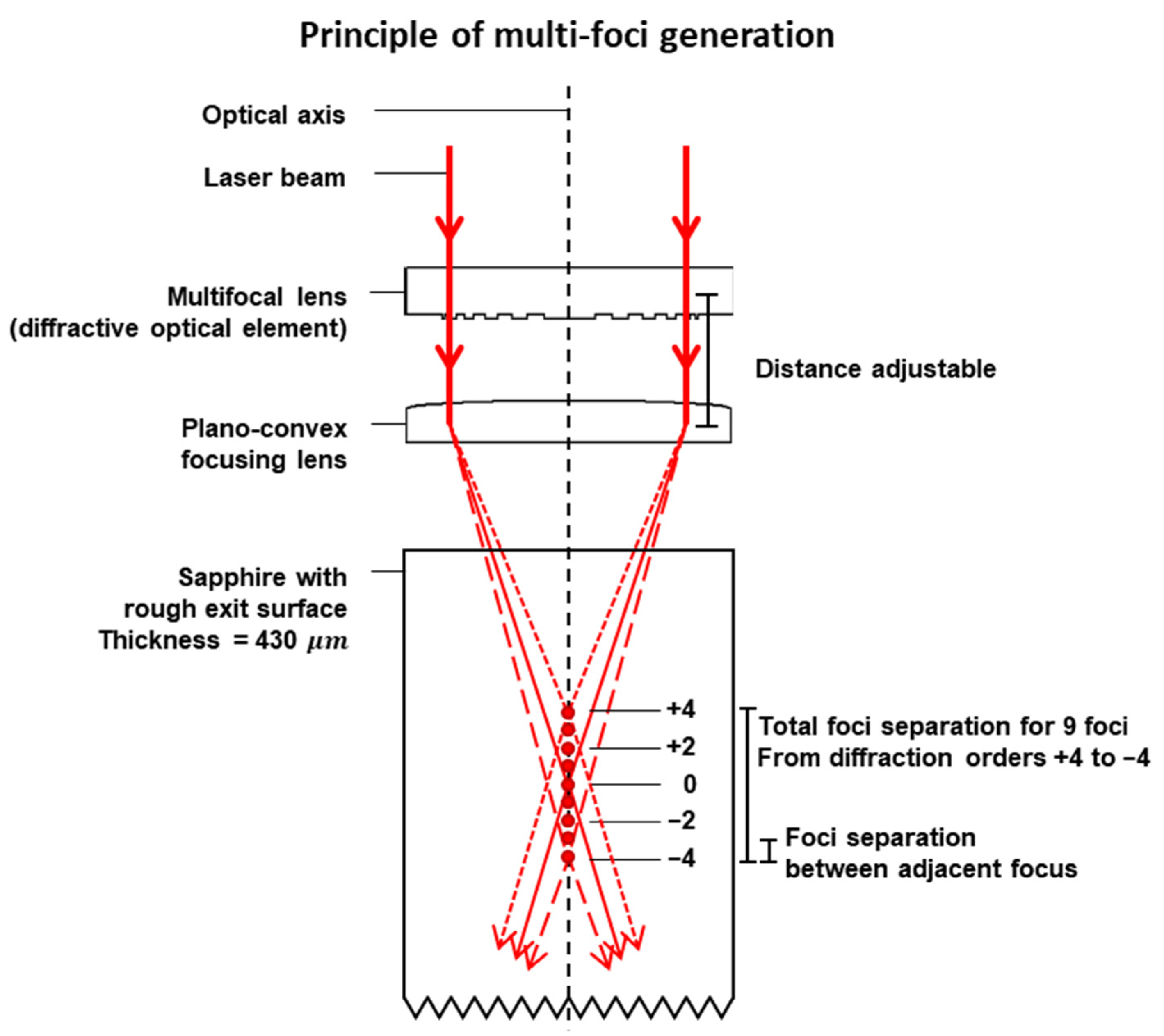
:1. Introduction
2. Materials and Methods
3. Results
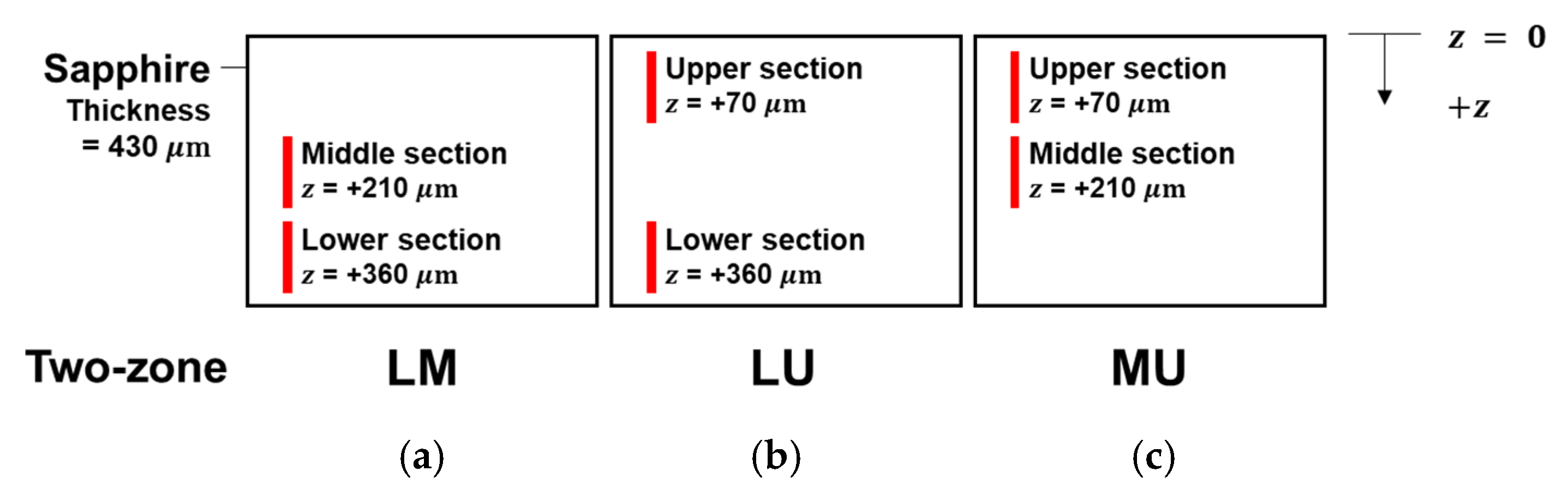
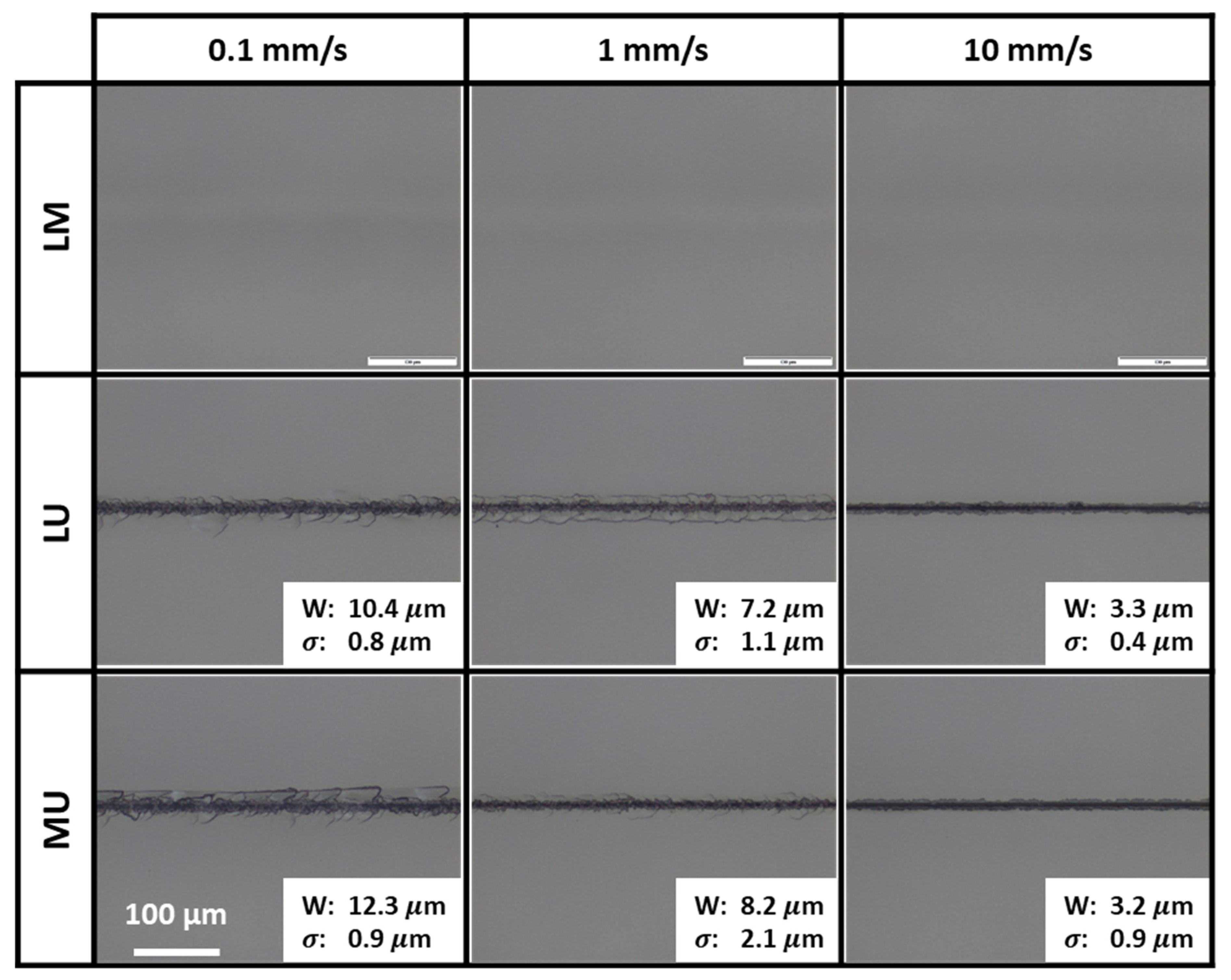
3.1. Top Polished Entry Surface for Two-Zone Scanning
3.1.1. Scribe Formation with Two-Zone LM (Lower-Middle Sections)
3.1.2. Scribe Formation with Two-Zone LU (Lower-Upper Sections)
3.1.3. Scribe Formation with Two-Zone MU (Middle-Upper Sections)
3.2. Bottom Rough Exit Surface Scribes
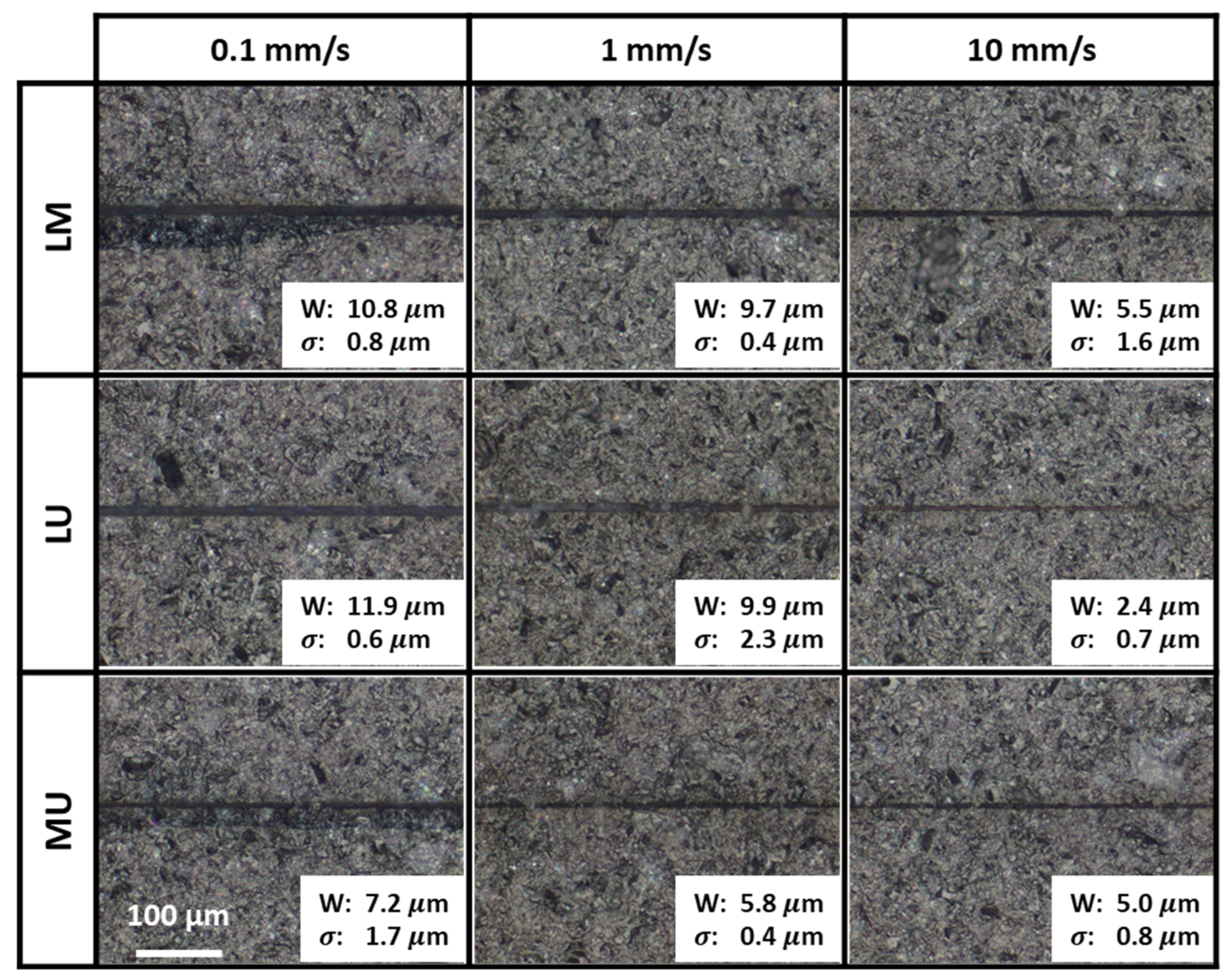
3.2.1. Scribe Formation with Two-Zone LM (Lower-Middle Sections)
3.2.2. Scribe Formation with Two-Zone LU (Lower-Upper Sections)
3.2.3. Scribe Formation with Two-Zone MU (Middle-Upper Sections)
3.3. Sample Separation and Sidewall Profiles
3.3.1. Unsuccessful Sample Separation with Two-Zone LM and LU
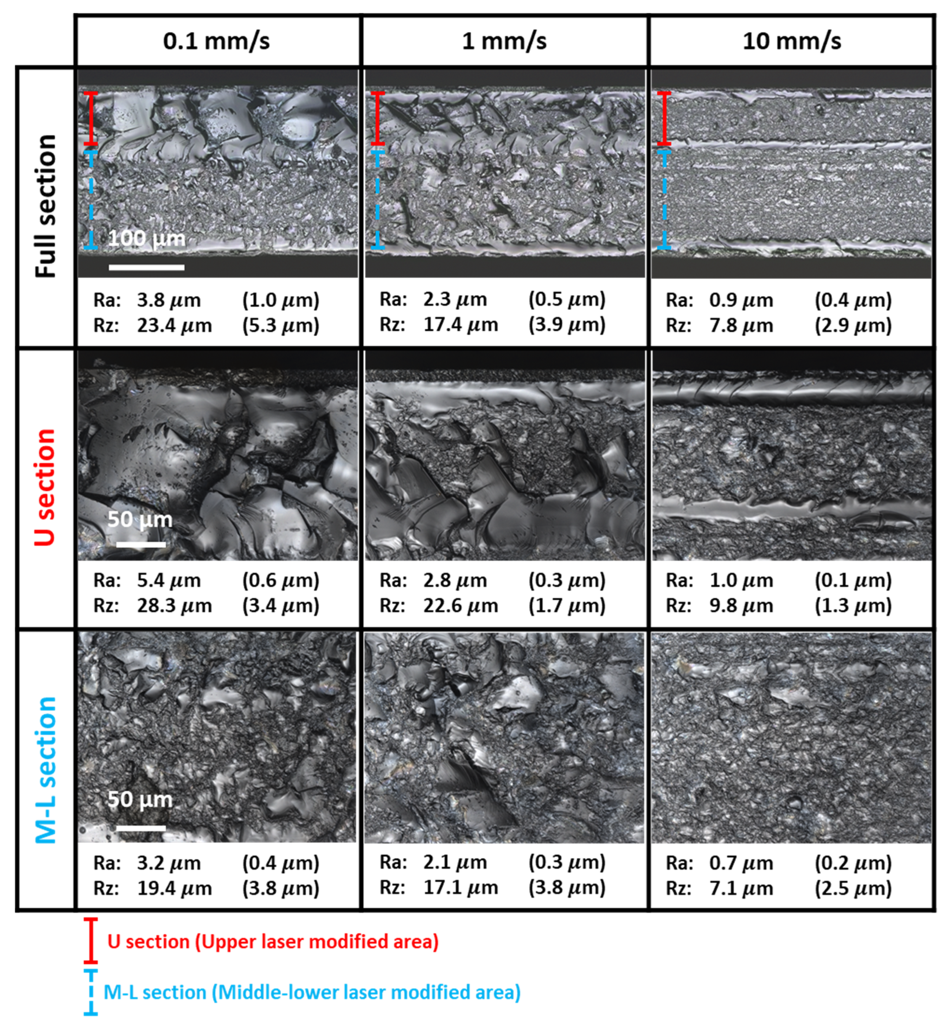
3.3.2. Sample Separation with Two-Zone MU (Middle-Upper Sections)
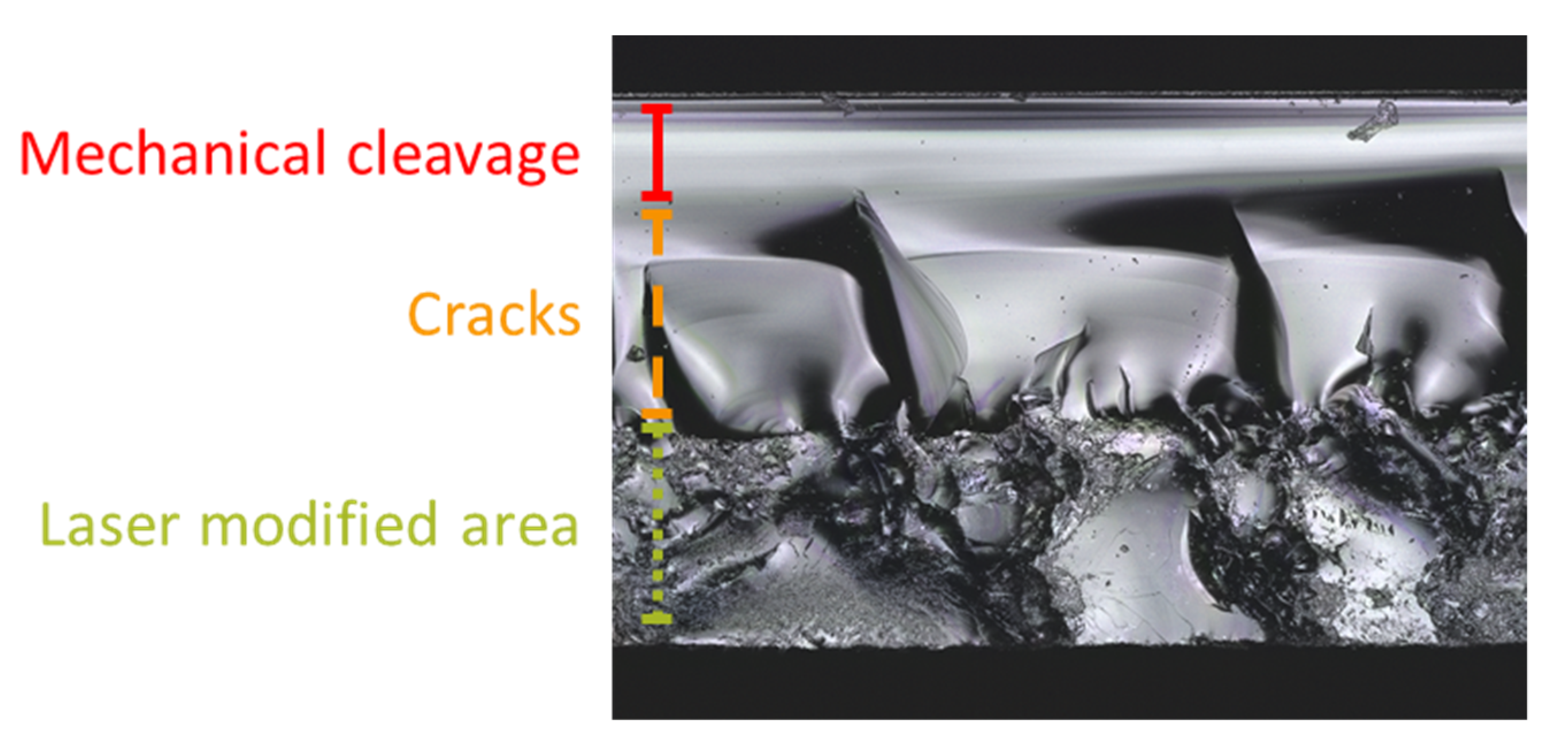
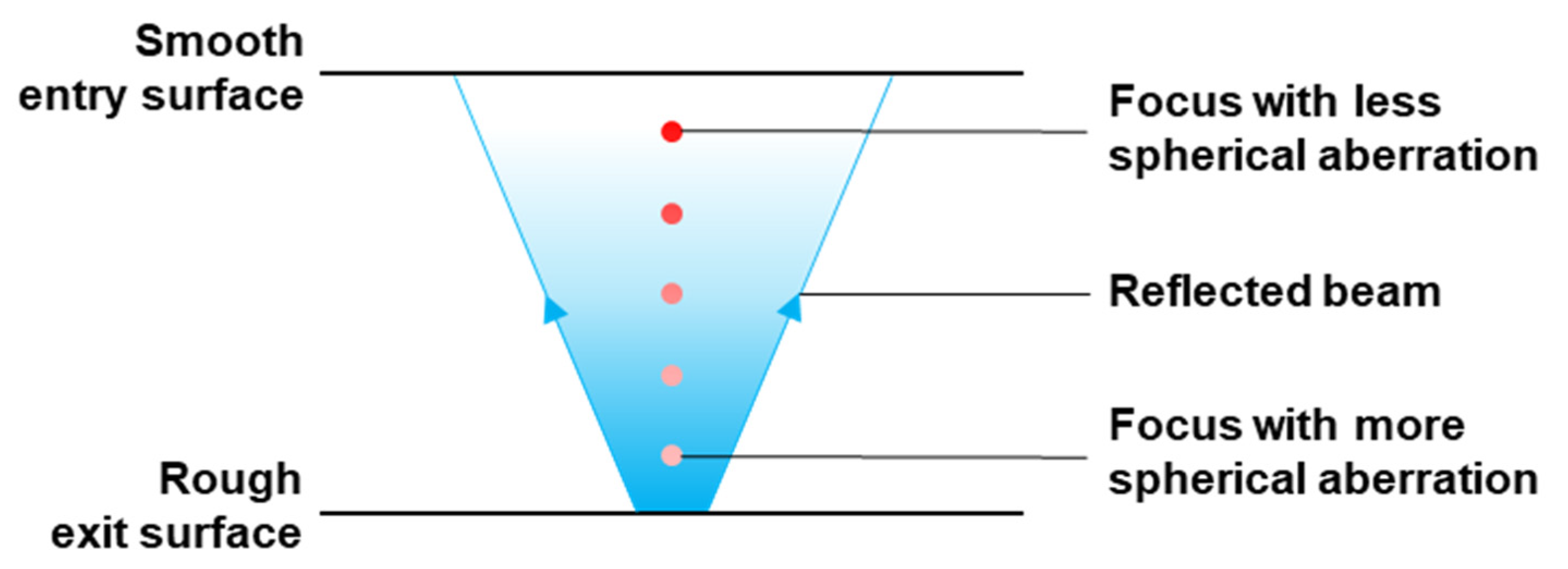
3.4. Spherical Aberration and Internal Reflection at the Exit Surface
4. Conclusions
Author Contributions
Funding
Data Availability Statement
Conflicts of Interest
References
- Kim, H.; Kim, D.; Kim, C.; Jeong, H. Multi-wire sawing of sapphire crystals with reciprocating motion of electroplated diamond wires. CIRP Ann. 2013, 62, 335–338. [Google Scholar] [CrossRef]
- Mizumoto, Y.; Maas, P.; Kakinuma, Y.; Min, S. Investigation of the cutting mechanisms and the anisotropic ductility of monocrystalline sapphire. CIRP Ann. 2017, 66, 89–92. [Google Scholar] [CrossRef]
- Li, Z.; Wang, X.; Wang, J.; Allegre, O.; Guo, W.; Gao, W.; Jia, N.; Li, L. Stealth dicing of sapphire sheets with low surface roughness, zero kerf width, debris/crack-free and zero taper using a femtosecond Bessel beam. Opt. Laser Technol. 2021, 135, 106713. [Google Scholar] [CrossRef]
- Gedvilas, M.; Mikšys, J.; Berzinš, J.; Stankevič, V.; Račiukaitis, G. Multi-photon absorption enhancement by dual-wavelength double-pulse laser irradiation for efficient dicing of sapphire wafers. Sci. Rep. 2017, 7, 5218. [Google Scholar] [CrossRef]
- Lee, J.-M.; Jang, J.-H.; Yoo, T.-K. Scribing and cutting a blue LED wafer using a Q-switched. Nd:YAG laser. Appl. Phys. A Mater. Sci. Process. 2000, 70, 561–564. [Google Scholar] [CrossRef]
- Li, Y.; Liu, H.; Hong, M. High-quality sapphire microprocessing by dual-beam laser induced plasma assisted ablation. Opt. Express 2020, 28, 6242–6250. [Google Scholar] [CrossRef] [PubMed]
- Xu, J.; Hu, H.; Zhuang, C.; Ma, G.; Han, J.; Lei, Y. Controllable laser thermal cleavage of sapphire wafers. Opt. Lasers Eng. 2018, 102, 26–33. [Google Scholar] [CrossRef]
- Benayas, A.; Jaque, D.; McMillen, B.; Chen, K.P. Thermal stability of microstructural and optical modifications induced in sapphire by ultrafast laser filamentation. J. Appl. Phys. 2010, 107, 33522. [Google Scholar] [CrossRef] [Green Version]
- Yan, T.; Ji, L.; Sun, W. Characteristics and formation mechanism of filamentary plasma string induced by single picosecond laser pulse in sapphire. Appl. Phys. A 2021, 128, 39. [Google Scholar] [CrossRef]
- Yadav, A.; Kbashi, H.; Kolpakov, S.; Gordon, N.; Zhou, K.; Rafailov, E.U. Stealth dicing of sapphire wafers with near infra-red femtosecond pulses. Appl. Phys. A Mater. Sci. Process. 2017, 123, 369. [Google Scholar] [CrossRef] [Green Version]
- Chang, S.J.C.; Chang, L.M.; Chen, J.Y.; Hsu, C.S.; Kuo, D.S.; Shen, C.F.; Chen, W.S.; Ko, T.K. GaN-Based Light-Emitting Diodes Prepared with Shifted Laser Stealth Dicing. J. Disp. Technol. 2016, 12, 195–199. [Google Scholar] [CrossRef]
- Zhang, Y.; Xie, H.; Zheng, H.; Wei, T.; Yang, H.; Li, J.; Yi, X.; Song, X.; Wang, G.; Li, J. Light extraction efficiency improvement by multiple laser stealth dicing in InGaN-based blue light-emitting diodes. Opt. Express 2012, 20, 6808–6815. [Google Scholar] [CrossRef]
- Liu, P.; Deng, L.; Duan, J.; Wu, B.; Zeng, X.; Shangguan, Y.; Wang, X. A study on laser multi-focus separation technology of thick KDP crystal. Int. J. Mach. Tools Manuf. 2017, 118–119, 26–36. [Google Scholar] [CrossRef]
- Liu, P.; Duan, J.; Wu, B.; Deng, L.; Shangguan, Y.; Zeng, X.; Wang, X. A flexible multi-focus laser separation technology for thick glass. Int. J. Mach. Tools Manuf. 2018, 135, 12–23. [Google Scholar] [CrossRef]
- Ma, R.; Ji, L.; Yan, T. Laser multi-focus precision cutting of thick sapphire by spherical aberration rectification. Opt. Lasers Eng. 2020, 126, 105876. [Google Scholar] [CrossRef]
- Lye, C.S.; Wang, Z.; Lam, Y.C. Multi-Foci Division of Nonlinear Energy Absorption on Ultrashort Pulse Laser Singulation of Sapphire Wafers. Micromachines 2021, 12, 1328. [Google Scholar] [CrossRef] [PubMed]
- Baylies, W.E.; Moore, C.J. The Use of Sapphire in Mobile Device and LED Industries|Semiconductor Digest. 2015. Available online: https://sst.semiconductor-digest.com/2015/11/the-use-of-sapphire-in-mobile-device-and-led-industries/ (accessed on 3 October 2018).
- Yamada, M.; Mitani, T.; Narukawa, Y.; Shioji, S.; Niki, I.; Sonobe, S.; Deguchi, K.; Sano, M.; Mukai, T. InGaN-Based Near-Ultraviolet and Blue-Light-Emitting Diodes with High External Quantum Efficiency Using a Patterned Sapphire Substrate and a Mesh Electrode. Jpn. J. Appl. Phys. 2002, 41, L1431. [Google Scholar] [CrossRef]
- Wuu, D.S.; Wang, W.K.; Shih, W.C.; Horng, R.H.; Lee, C.E.; Lin, W.Y.; Fang, J.S. Enhanced output power of near-ultraviolet InGaN-GaN LEDs grown on patterned sapphire substrates. IEEE Photonics Technol. Lett. 2005, 17, 288–290. [Google Scholar] [CrossRef]
- Yang, G.; Chang, J.; Zhao, J.; Tong, Y.; Xie, F.; Wang, J.; Zhang, Q.; Huang, H.; Yan, D. Investigation of light output performance for gallium nitride-based light-emitting diodes grown on different shapes of patterned sapphire substrate. Mater. Sci. Semicond. Process. 2015, 33, 149–153. [Google Scholar] [CrossRef]
- Wang, M.-S.; Huang, X.-J.; Yang, L. Performance enhancement by different sidewall structures for InGaN-based light-emitting diodes. J. Mater. Sci. Mater. Electron. 2014, 25, 3645–3651. [Google Scholar] [CrossRef]
- Guo, Y.; Zhang, Y.; Yan, J.; Chen, X.; Zhang, S.; Xie, H.; Liu, P.; Zhu, H.; Wang, J.; Li, J. Sapphire substrate sidewall shaping of deep ultraviolet light-emitting diodes by picosecond laser multiple scribing. Appl. Phys. Express 2017, 10, 62101. [Google Scholar] [CrossRef]
- Lye, C.S.M.; Wang, Z.K.; Lam, Y.C. Mechanism and effects of surface morphology on absorption characteristics in ultrashort pulse laser processing of sapphire. Appl. Surf. Sci. 2021, 542, 148734. [Google Scholar] [CrossRef]
- HOLO/OR Ltd. MultiFocal DOEs-Holo Or-Diffractive Optics. Available online: https://www.holoor.co.il/product/multifocal/ (accessed on 17 October 2018).
- Lam, H.M.; Hong, M.; Yuan, S.; Chong, T.C. Laser ablation of GaN/sapphire structure for LED. In Proceedings of the LAMP 2002: International Congress on Laser Advanced Materials Processing, Osaka, Japan, 19 February 2003; Volume 4830. [Google Scholar] [CrossRef]


| Scanning Speed (mm/s) | Energy Deposited at a Single Spot (mJ) | Pulse Overlap |
|---|---|---|
| 0.1 | 12.5 | 1100 |
| 1 | 1.25 | 110 |
| 10 | 0.13 | 11 |
| Scanning Zones | Scanning Speed (mm/s) | ||
|---|---|---|---|
| 0.1 | 1 | 10 | |
| LM | No cleavage | No cleavage | No cleavage |
| LU | No cleavage | No cleavage | No cleavage |
| MU | Sample cleaved | Sample cleaved | Sample cleaved |
| Feature | Ra (μm) | Rz (μm) | ||
|---|---|---|---|---|
| Average | Std. Dev | Average | Std. Dev | |
| Mechanical cleavage | 0.5 | 0.3 | 2.4 | 1.6 |
| Cracks | 9.0 | 0.7 | 40.5 | 1.7 |
| Laser-modified area | 2.6 | 0.4 | 20.6 | 3.7 |
| Laser Dicing Method | No. of Foci/Pass | Scanning Speed (mm/s) | Sample Thickness (μm) | Scanned Section (μm) | Sidewall Roughness (μm) | Uniformity of Sidewall | |
|---|---|---|---|---|---|---|---|
| Ave | Std. Dev | ||||||
| Bessel beam [3] | - | 0.1–7 | 380, 1000, 1500 | Full thickness | 0.2–1.3 | - | - |
| Femtosecond laser ablation [25] | 1 | 2 | ~339 | - | 4.13 | - | Visually uniform |
| Partial thickness multi-foci dicing (previous work) [16] | 15 | 1 | 430 | 136 (1 section scanned) | 2.6 | 0.4 | Mechanical cleavage, cracks, non-uniform laser modification |
| Full thickness multi-foci dicing [15] | 21 | 4 | 2000 | Full thickness | 4.5 | - | Mechanical cleavage, non-uniform laser modification |
| Full thickness multi-foci dicing [15] | 21 | 4 | 500 | Full thickness | 3.2 | - | Visually uniform |
| Sectional multi-foci dicing [15] | 15 | 4 | 2000 | 500 (4 sections scanned) | 2.5 | - | No micro-cracks reported |
| Partial thickness multi-foci dicing (current work) | 9 | 10 | 430 | 136 (2 sections scanned) | 0.9 | 0.4 | Mechanical cleavage, visually uniform laser modification |
Publisher’s Note: MDPI stays neutral with regard to jurisdictional claims in published maps and institutional affiliations. |
© 2022 by the authors. Licensee MDPI, Basel, Switzerland. This article is an open access article distributed under the terms and conditions of the Creative Commons Attribution (CC BY) license (https://creativecommons.org/licenses/by/4.0/).
Share and Cite
Lye, C.S.M.; Wang, Z.; Lam, Y.C. Multi-Foci Laser Separation of Sapphire Wafers with Partial Thickness Scanning. Micromachines 2022, 13, 506. https://doi.org/10.3390/mi13040506
Lye CSM, Wang Z, Lam YC. Multi-Foci Laser Separation of Sapphire Wafers with Partial Thickness Scanning. Micromachines. 2022; 13(4):506. https://doi.org/10.3390/mi13040506
Chicago/Turabian StyleLye, Celescia Siew Mun, Zhongke Wang, and Yee Cheong Lam. 2022. "Multi-Foci Laser Separation of Sapphire Wafers with Partial Thickness Scanning" Micromachines 13, no. 4: 506. https://doi.org/10.3390/mi13040506
APA StyleLye, C. S. M., Wang, Z., & Lam, Y. C. (2022). Multi-Foci Laser Separation of Sapphire Wafers with Partial Thickness Scanning. Micromachines, 13(4), 506. https://doi.org/10.3390/mi13040506