
Realization of Three-Dimensionally MEMS Stacked Comb Structures for Microactuators Using Low-Temperature Multi-Wafer Bonding with Self-Alignment Techniques in CMOS-Compatible Processes


Abstract
:1. Introduction
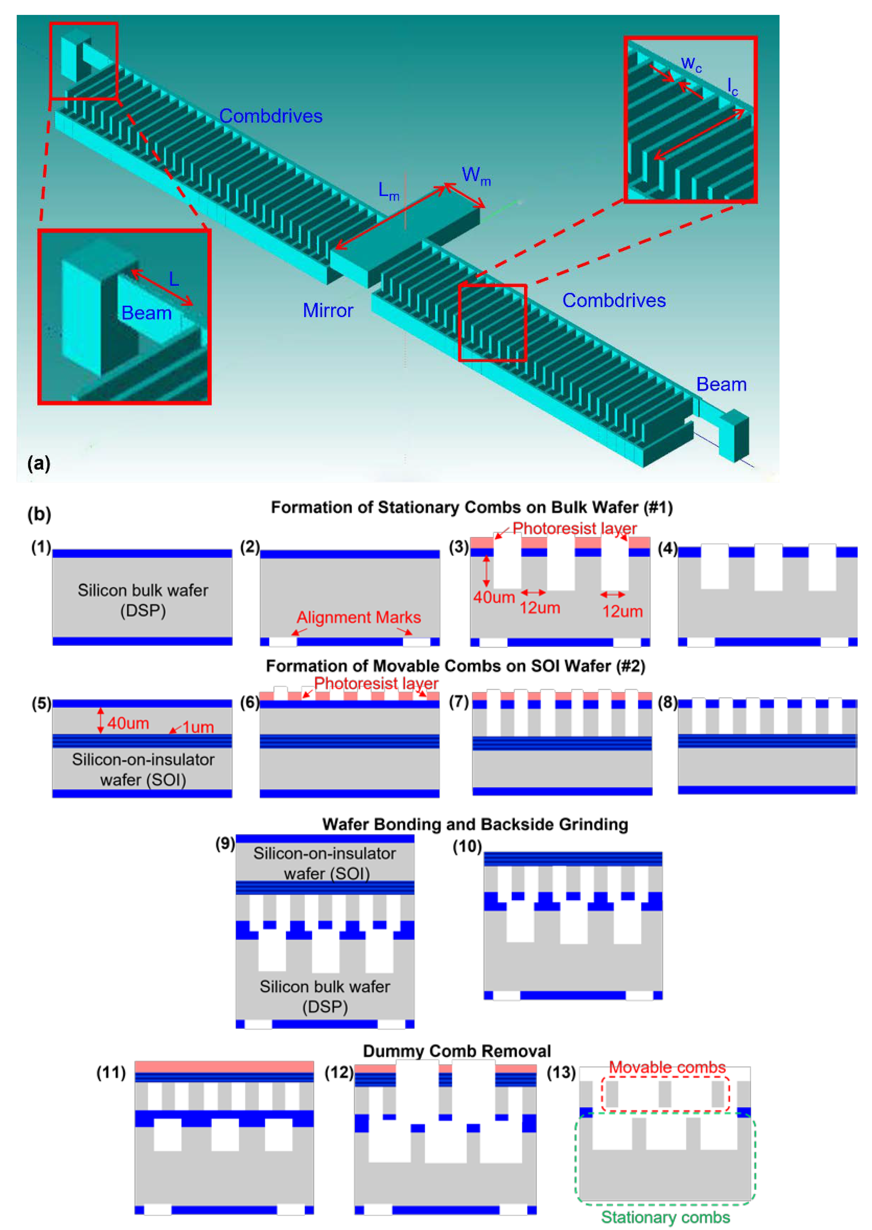
2. Device and Process Flow Design
3. Fabrication Results
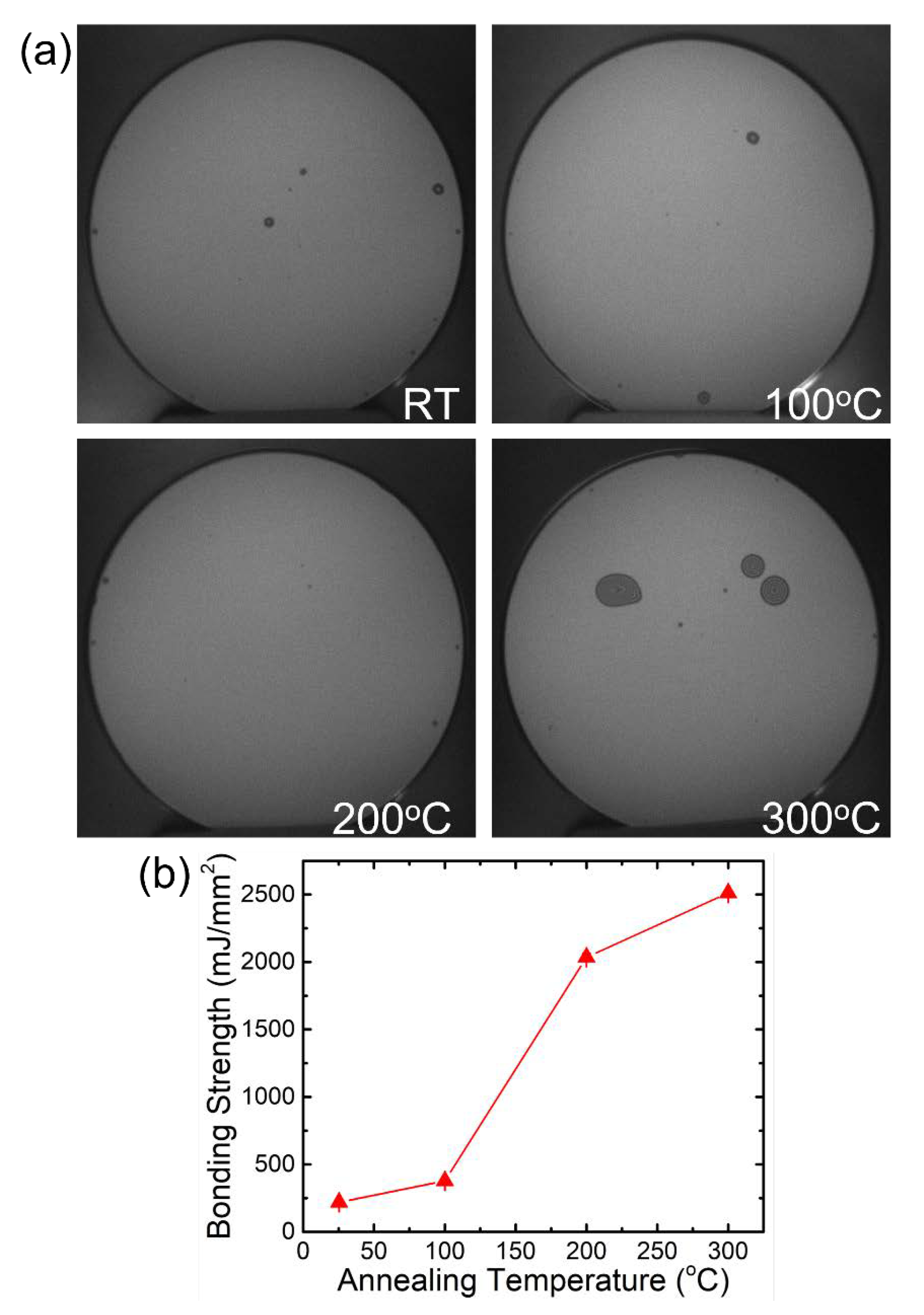
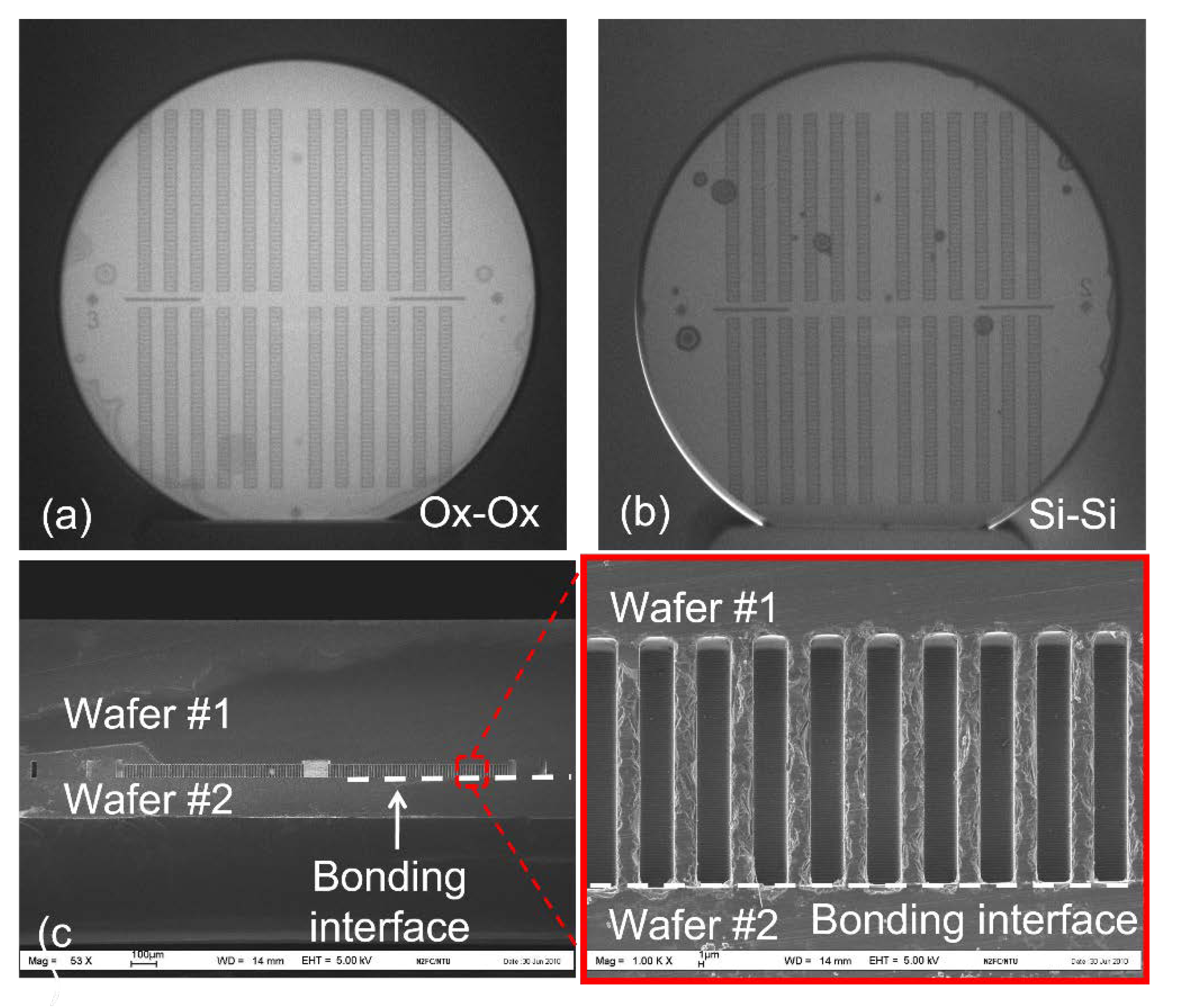
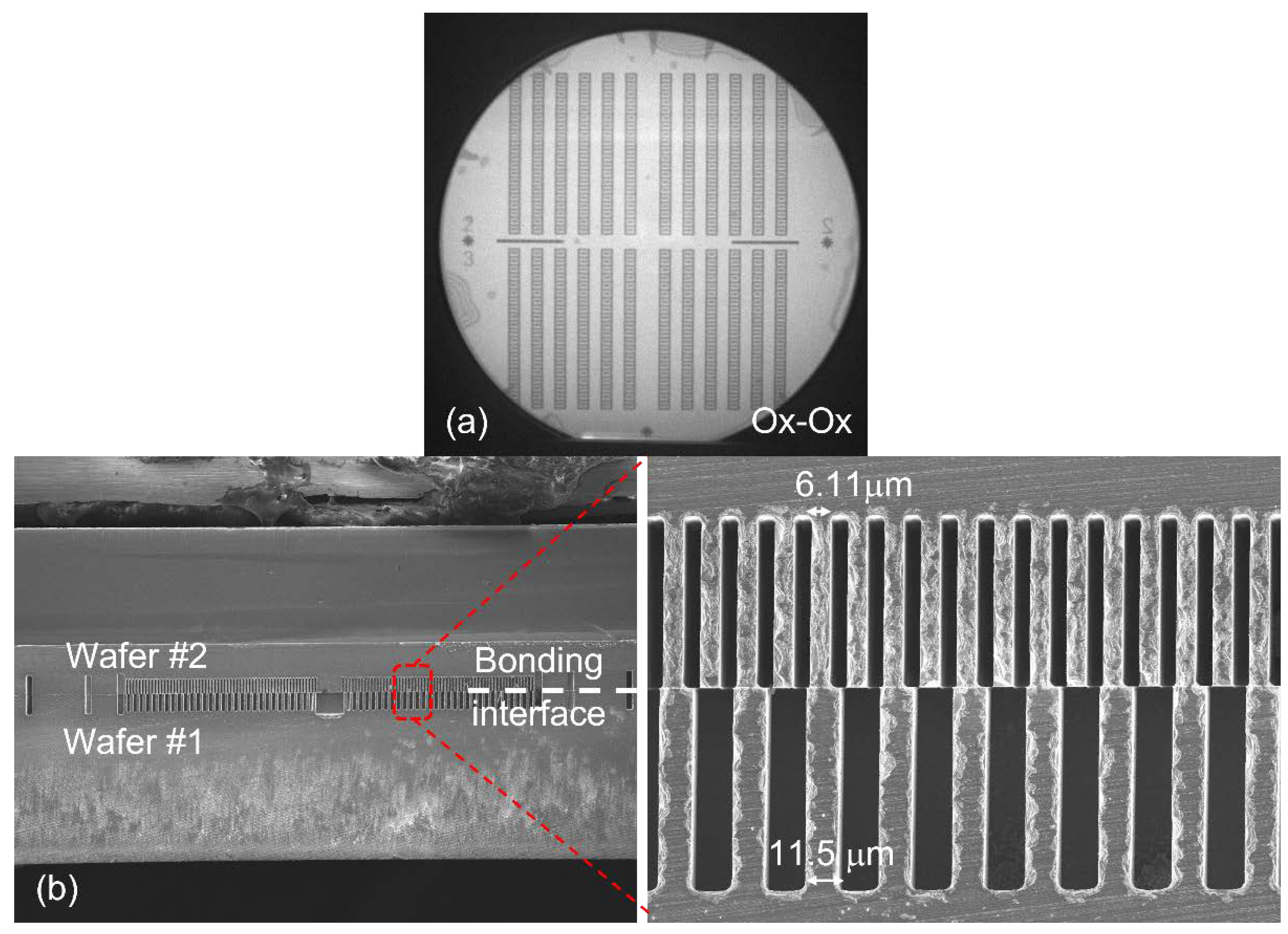
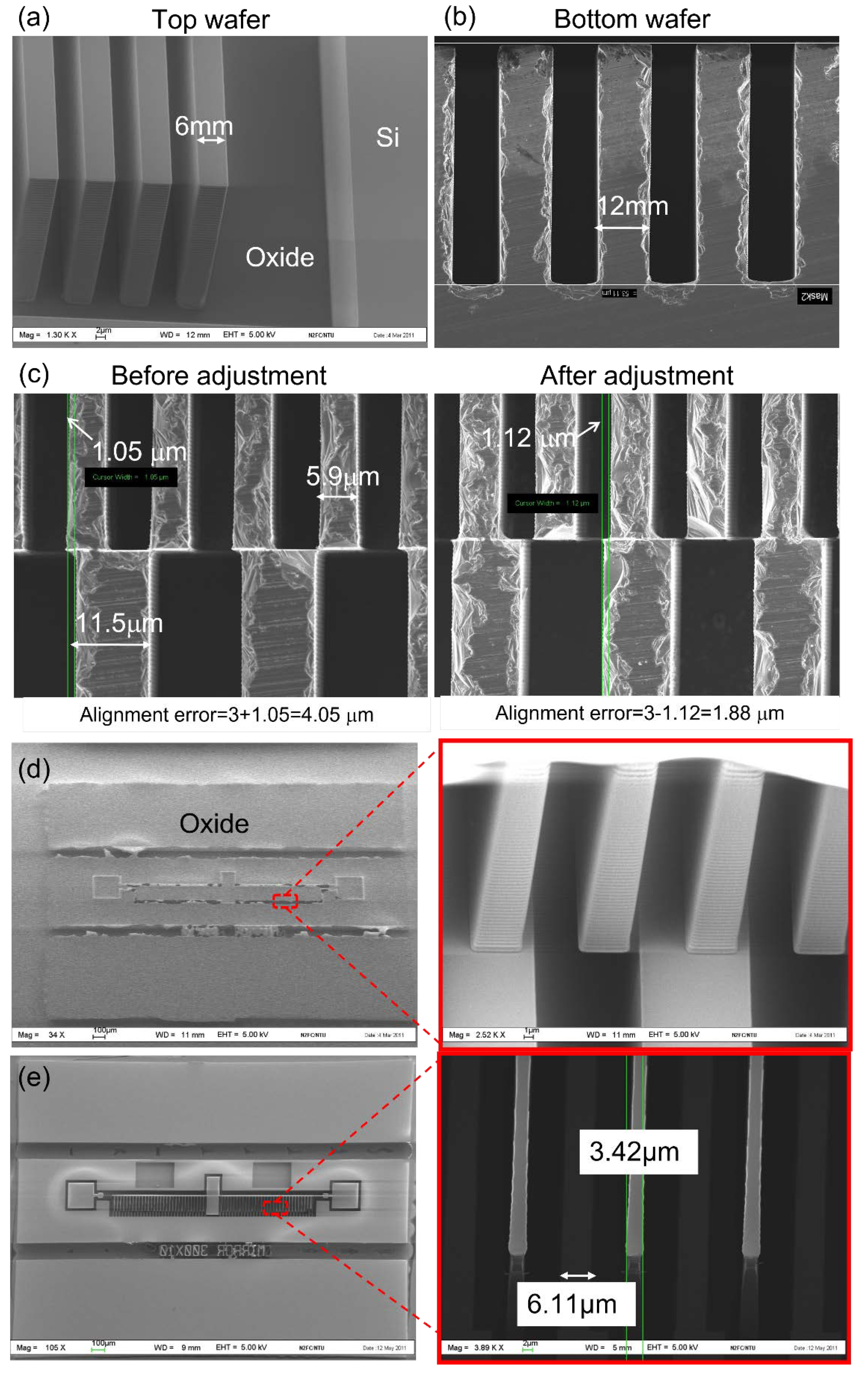
3.1. Wafer Bonding
3.2. Device Fabrication
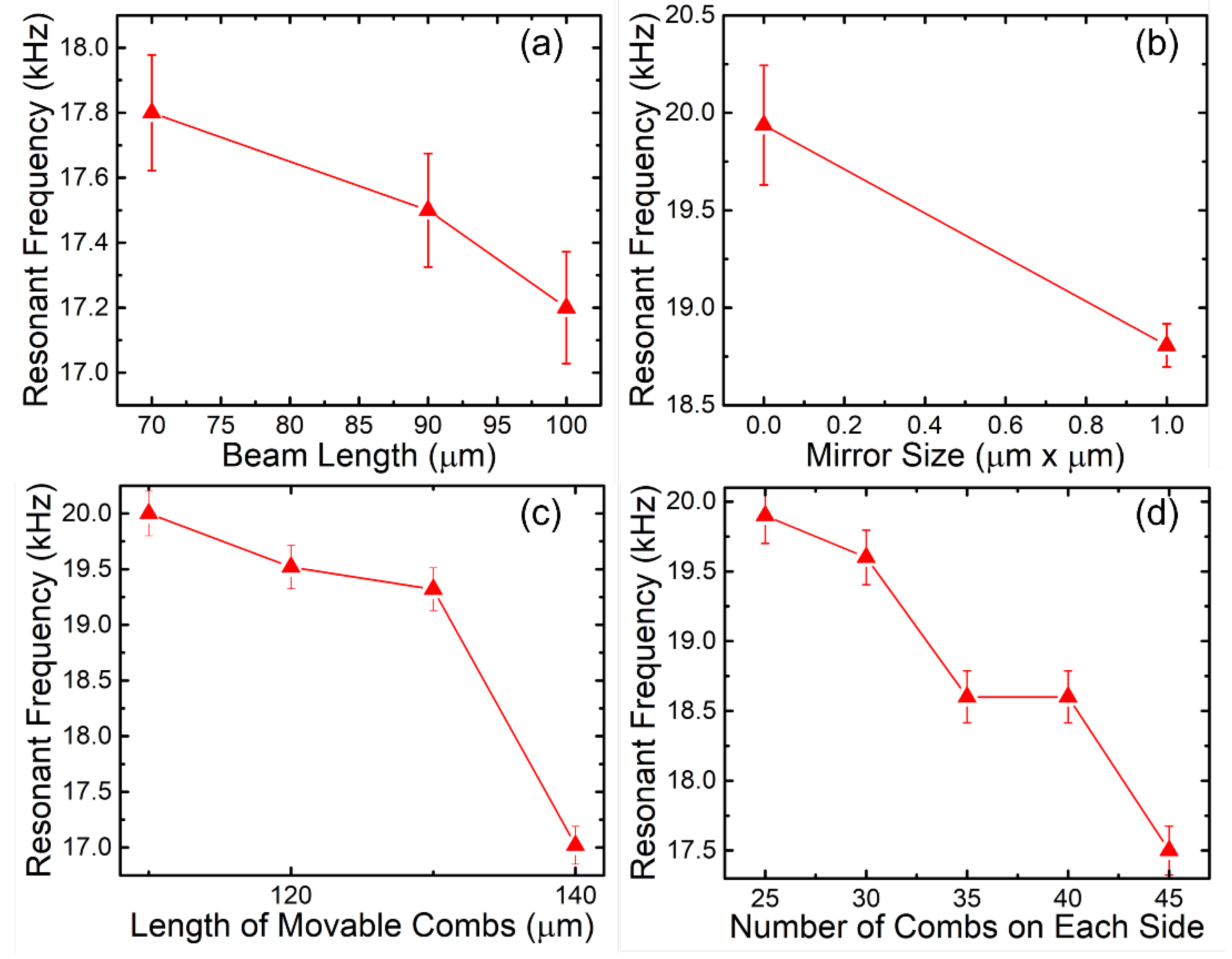
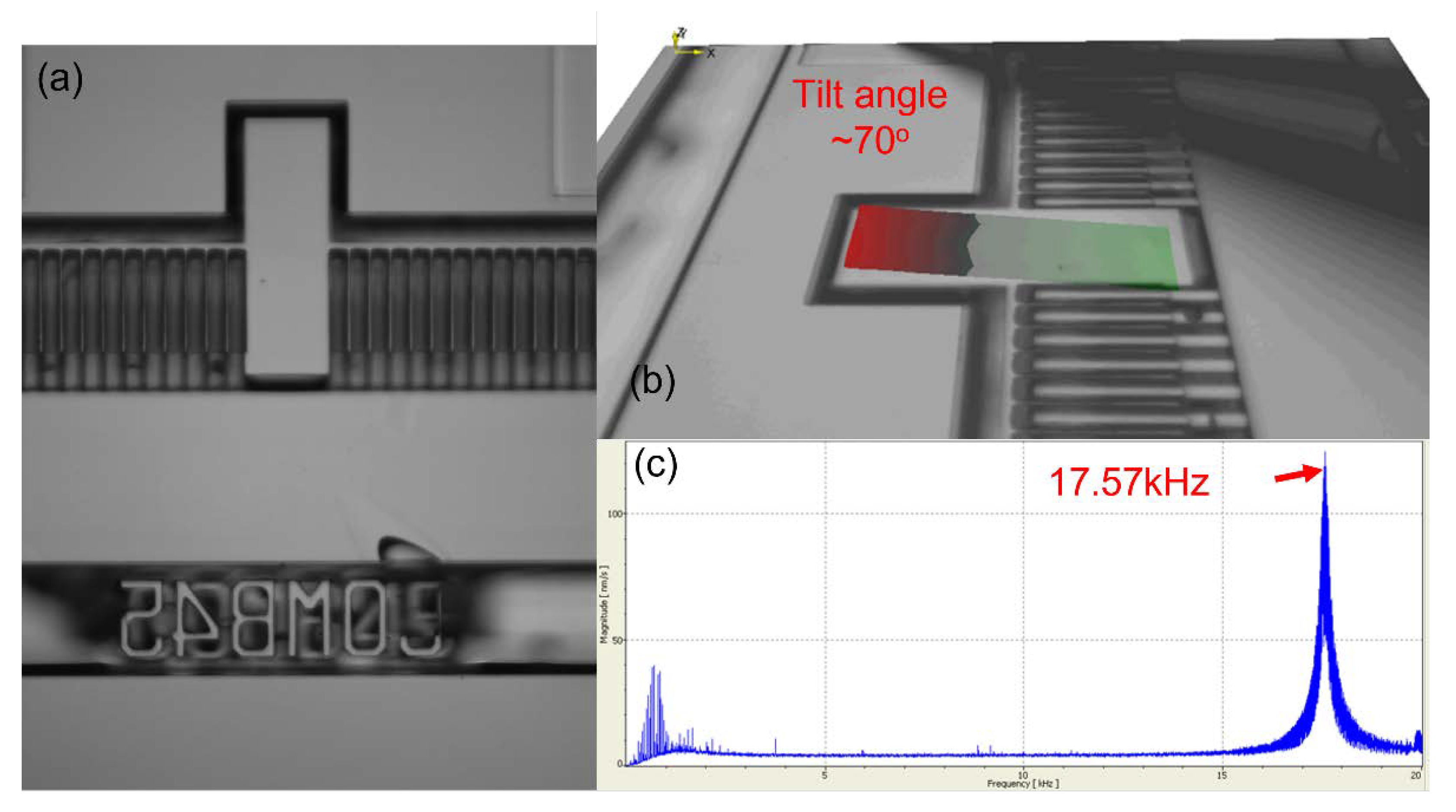
4. Device Performance
5. Conclusions and Summary
Author Contributions
Funding
Data Availability Statement
Acknowledgments
Conflicts of Interest
References
- Feynman, R.P. Plenty of Room at the Bottom. In Proceedings of the APS Annual Meeting, Pasadena, CA, USA, 29 December 1959. [Google Scholar]
- Chow, C.L.; Li, K.H.H. MEMS Inertia Sensors in Semi-Standard Processes–Transiting from University’s Laboratory to a CMOS-MEMS Foundry. In Proceedings of the 2019 Symposium on Design, Test, Integration & Packaging of MEMS and MOEMS (DTIP), Paris, France, 12–15 May 2019; pp. 1–4. [Google Scholar]
- Hocheol, L.; Michele, H.M.; Thomas, G.B. CMOS chip planarization by chemical mechanical polishing for a vertically stacked metal MEMS integration. J. Micromechanics Microengineering 2020, 14, 108–115. [Google Scholar]
- Classen, J.; Reinmuth, J.; Kälberer, A.; Scheurle, A.; Günther, S.; Kiesel, S.; Schellin, B.; Bräuer, J.; Eicher, L. Advanced surface micromachining process—A first step towards 3D MEMS. In Proceedings of the 2017 IEEE 30th International Conference on Micro Electro Mechanical Systems (MEMS), Las Vegas, NV, USA, 22–26 January 2017; pp. 314–318. [Google Scholar]
- Le, H.T.; Mizushima, I.; Nour, Y.; Tang, P.T.; Knott, A.; Ouyang, Z.; Jensen, F.; Han, A. Fabrication of 3D air-core MEMS inductors for very-high-frequency power conversions. Microsyst. Nanoeng. 2018, 4, 1–9. [Google Scholar] [CrossRef] [Green Version]
- Miki, N.; Zhang, X.; Khanna, R.; Ayón, A.; Ward, D.; Spearing, S. Multi-stack silicon-direct wafer bonding for 3D MEMS manufacturing. Sens. Actuators A: Phys. 2003, 103, 194–201. [Google Scholar] [CrossRef]
- Narasimhan, V.; Li, H.; Tan, C.S. Monolithic CMOS-MEMS integration for high-g accelerometers. In Proceedings of the Emerging Technologies in Security and Defence II; and Quantum-Physics-Based Information Security III, Amsterdam, Netherlands, 22–23 September 2014; p. 925410. [Google Scholar]
- Cheng, Z.; Toshiyoshi, H. CMOS-MEMS Micro-Mirror Arrays by Post-Processing ASMC 0.35-μm CMOS Chips. J. Microelectromechanical Syst. 2017, 26, 1435–1441. [Google Scholar] [CrossRef]
- Yoo, H.W.; Druml, N.; Brunner, D.; Schwarzl, C.; Thurner, T.; Hennecke, M.; Schitter, G. MEMS-based lidar for autonomous driving. E I Elektrotechnik Und Inf. 2018, 135, 408–415. [Google Scholar] [CrossRef] [Green Version]
- Mita, M.; Miyauchi, D.; Toshiyoshi, H.; Fujita, H. An out-of-plane polysilicon actuator with a smooth vertical mirror for optical fiber switch application. In Proceedings of the IEEE/LEOS Summer Topical Meetings, Monterey, CA, USA, 20–24 July 1998; pp. 33–34. [Google Scholar]
- Piyawattanametha, W.; Patterson, P.R.; Hah, D.; Toshiyoshi, H.; Wu, M.C. A 2D scanner by surface and bulk micromachined vertical comb actuators. In Proceedings of the 2003 IEEE/LEOS International Conference on Optical MEMS (Cat. No. 03EX682), Piscataway, NJ, USA, 18–21 August 2003; pp. 93–94. [Google Scholar]
- Molfese, A.; Nannini, A.; Pennelli, G.; Pieri, F. Analysis, testing and optimisation of electrostatic comb-drive levitational actuators. Analog. Integr. Circuits Signal. Process. 2006, 48, 33–40. [Google Scholar] [CrossRef]
- Hah, D.; Choi, C.-A.; Kim, C.-K.; Jun, C.-H. A self-aligned vertical comb-drive actuator on an SOI wafer for a 2D scanning micromirror. J. Micromechanics Microengineering 2004, 14, 1148. [Google Scholar] [CrossRef]
- Galchev, T.; Welch, W.; Najafi, K. A new low-temperature high-aspect-ratio MEMS process using plasma activated wafer bonding. J. Micromechanics Microengineering 2011, 21, 045020. [Google Scholar] [CrossRef]
- Chu, C.C.; Tsai, J.M.; Hsieh, J.; Fang, W. A novel electrostatic vertical comb actuator fabricated on [111] silicon wafer. In Proceedings of the The Sixteenth Annual International Conference on Micro Electro Mechanical Systems, 2003. MEMS-03 Kyoto. IEEE, Kyoto, Japan, 19–23 January 2003; pp. 56–59. [Google Scholar]
- Krishnamoorthy, U.; Lee, D.; Solgaard, O. Self-aligned vertical electrostatic combdrives for micromirror actuation. J. Microelectromechanical Syst. 2003, 12, 458–464. [Google Scholar] [CrossRef]
- Tan, C.; Fan, A.; Chen, K.-N.; Reif, R. Low-temperature thermal oxide to plasma-enhanced chemical vapor deposition oxide wafer bonding for thin-film transfer application. Appl. Phys. Lett. 2003, 82, 2649–2651. [Google Scholar] [CrossRef] [Green Version]
- Chong, G.; Tan, C. Low temperature PE-TEOS oxide bonding assisted by a thin layer of high-κ dielectric. Electrochem. Solid State Lett. 2009, 12, H408. [Google Scholar] [CrossRef]
- Kuhne, S.; Blattmann, R.; Hierold, C. Low temperature fabrication process for high-aspect-ratio and multi-compliant MEMS. In Proceedings of the 2009 IEEE 22nd International Conference on Micro Electro Mechanical Systems, Sorrento, Italy, 25–29 January 2009; pp. 673–676. [Google Scholar]
- Tan, C.S.; Fan, J.; Lim, D.F.; Chong, G.Y.; Li, K.H. Low temperature wafer-level bonding for hermetic packaging of 3D microsystems. J. Micromechanics Microengineering 2011, 21, 075006. [Google Scholar] [CrossRef]
- Young, W.C.; Budynas, R.G.; Sadegh, A.M. Roark’s Formulas for Stress and Strain; McGraw-hill New York: New York, NY, USA, 2002; Volume 7. [Google Scholar]
- Conant, R.A. Micromachined Mirrors; University of California, Berkeley: Berkeley, CA, USA, 2002. [Google Scholar]
- Tsai, C.-C.; Li, Z.-H.; Lin, Y.-T.; Lu, M.S.-C. A closed-loop controlled CMOS MEMS biaxial scanning mirror for projection displays. IEEE Sens. J. 2019, 20, 242–249. [Google Scholar] [CrossRef]


| Device Parameter | Nominal Value | Description |
|---|---|---|
| Lm | 300 µm | Mirror length |
| Wm | 100 µm | Mirror width |
| lc | 120 µm | Comb finger length |
| wc | 6 µm | Comb finger width |
| g | 6 µm | Gap between comb fingers |
| N | 60 | The number of comb fingers |
| L | 45 µm | Beam length |
| Wb | 4 µm | Beam width |
| t | 40 µm | Thickness of beam, comb and mirror |
Publisher’s Note: MDPI stays neutral with regard to jurisdictional claims in published maps and institutional affiliations. |
© 2021 by the authors. Licensee MDPI, Basel, Switzerland. This article is an open access article distributed under the terms and conditions of the Creative Commons Attribution (CC BY) license (https://creativecommons.org/licenses/by/4.0/).
Share and Cite
Teo, A.J.T.; Li, K.H.H. Realization of Three-Dimensionally MEMS Stacked Comb Structures for Microactuators Using Low-Temperature Multi-Wafer Bonding with Self-Alignment Techniques in CMOS-Compatible Processes. Micromachines 2021, 12, 1481. https://doi.org/10.3390/mi12121481
Teo AJT, Li KHH. Realization of Three-Dimensionally MEMS Stacked Comb Structures for Microactuators Using Low-Temperature Multi-Wafer Bonding with Self-Alignment Techniques in CMOS-Compatible Processes. Micromachines. 2021; 12(12):1481. https://doi.org/10.3390/mi12121481
Chicago/Turabian StyleTeo, Adrian J. T., and King Ho Holden Li. 2021. "Realization of Three-Dimensionally MEMS Stacked Comb Structures for Microactuators Using Low-Temperature Multi-Wafer Bonding with Self-Alignment Techniques in CMOS-Compatible Processes" Micromachines 12, no. 12: 1481. https://doi.org/10.3390/mi12121481
APA StyleTeo, A. J. T., & Li, K. H. H. (2021). Realization of Three-Dimensionally MEMS Stacked Comb Structures for Microactuators Using Low-Temperature Multi-Wafer Bonding with Self-Alignment Techniques in CMOS-Compatible Processes. Micromachines, 12(12), 1481. https://doi.org/10.3390/mi12121481